EP1447694A1 - Optical via for transmission of signals through a printed circuit board - Google Patents
Optical via for transmission of signals through a printed circuit board Download PDFInfo
- Publication number
- EP1447694A1 EP1447694A1 EP03021693A EP03021693A EP1447694A1 EP 1447694 A1 EP1447694 A1 EP 1447694A1 EP 03021693 A EP03021693 A EP 03021693A EP 03021693 A EP03021693 A EP 03021693A EP 1447694 A1 EP1447694 A1 EP 1447694A1
- Authority
- EP
- European Patent Office
- Prior art keywords
- optical
- waveguide
- signal
- hole
- printed circuit
- Prior art date
- Legal status (The legal status is an assumption and is not a legal conclusion. Google has not performed a legal analysis and makes no representation as to the accuracy of the status listed.)
- Granted
Links
- 230000003287 optical effect Effects 0.000 title claims abstract description 173
- 230000008054 signal transmission Effects 0.000 title claims 2
- 230000005693 optoelectronics Effects 0.000 claims abstract description 19
- 238000005253 cladding Methods 0.000 claims description 20
- 239000000463 material Substances 0.000 claims description 12
- 238000000034 method Methods 0.000 claims description 7
- 239000011248 coating agent Substances 0.000 claims description 5
- 238000000576 coating method Methods 0.000 claims description 5
- 230000008878 coupling Effects 0.000 claims description 3
- 238000010168 coupling process Methods 0.000 claims description 3
- 238000005859 coupling reaction Methods 0.000 claims description 3
- 239000000758 substrate Substances 0.000 claims 10
- 239000010410 layer Substances 0.000 description 21
- BWWVXHRLMPBDCK-UHFFFAOYSA-N 1,2,4-trichloro-5-(2,6-dichlorophenyl)benzene Chemical compound C1=C(Cl)C(Cl)=CC(Cl)=C1C1=C(Cl)C=CC=C1Cl BWWVXHRLMPBDCK-UHFFFAOYSA-N 0.000 description 8
- 239000000969 carrier Substances 0.000 description 4
- 230000005540 biological transmission Effects 0.000 description 3
- 238000005530 etching Methods 0.000 description 3
- 238000004519 manufacturing process Methods 0.000 description 3
- 230000010287 polarization Effects 0.000 description 3
- 150000003071 polychlorinated biphenyls Chemical class 0.000 description 3
- RYGMFSIKBFXOCR-UHFFFAOYSA-N Copper Chemical compound [Cu] RYGMFSIKBFXOCR-UHFFFAOYSA-N 0.000 description 2
- 229910052802 copper Inorganic materials 0.000 description 2
- 239000010949 copper Substances 0.000 description 2
- 239000002184 metal Substances 0.000 description 2
- 229910052751 metal Inorganic materials 0.000 description 2
- 229920000642 polymer Polymers 0.000 description 2
- 230000008569 process Effects 0.000 description 2
- 239000004593 Epoxy Substances 0.000 description 1
- 230000008859 change Effects 0.000 description 1
- 238000001816 cooling Methods 0.000 description 1
- 238000005520 cutting process Methods 0.000 description 1
- 230000007547 defect Effects 0.000 description 1
- 238000001514 detection method Methods 0.000 description 1
- 238000005516 engineering process Methods 0.000 description 1
- 239000000835 fiber Substances 0.000 description 1
- 239000012530 fluid Substances 0.000 description 1
- 239000011521 glass Substances 0.000 description 1
- 238000000608 laser ablation Methods 0.000 description 1
- 230000005012 migration Effects 0.000 description 1
- 238000013508 migration Methods 0.000 description 1
- 238000012986 modification Methods 0.000 description 1
- 230000004048 modification Effects 0.000 description 1
- 239000013307 optical fiber Substances 0.000 description 1
- 238000007747 plating Methods 0.000 description 1
- 239000002344 surface layer Substances 0.000 description 1
Images

Classifications
-
- H—ELECTRICITY
- H04—ELECTRIC COMMUNICATION TECHNIQUE
- H04B—TRANSMISSION
- H04B10/00—Transmission systems employing electromagnetic waves other than radio-waves, e.g. infrared, visible or ultraviolet light, or employing corpuscular radiation, e.g. quantum communication
- H04B10/80—Optical aspects relating to the use of optical transmission for specific applications, not provided for in groups H04B10/03 - H04B10/70, e.g. optical power feeding or optical transmission through water
- H04B10/801—Optical aspects relating to the use of optical transmission for specific applications, not provided for in groups H04B10/03 - H04B10/70, e.g. optical power feeding or optical transmission through water using optical interconnects, e.g. light coupled isolators, circuit board interconnections
-
- H—ELECTRICITY
- H05—ELECTRIC TECHNIQUES NOT OTHERWISE PROVIDED FOR
- H05K—PRINTED CIRCUITS; CASINGS OR CONSTRUCTIONAL DETAILS OF ELECTRIC APPARATUS; MANUFACTURE OF ASSEMBLAGES OF ELECTRICAL COMPONENTS
- H05K1/00—Printed circuits
- H05K1/02—Details
- H05K1/0274—Optical details, e.g. printed circuits comprising integral optical means
-
- G—PHYSICS
- G02—OPTICS
- G02B—OPTICAL ELEMENTS, SYSTEMS OR APPARATUS
- G02B6/00—Light guides; Structural details of arrangements comprising light guides and other optical elements, e.g. couplings
- G02B6/24—Coupling light guides
- G02B6/42—Coupling light guides with opto-electronic elements
- G02B6/4201—Packages, e.g. shape, construction, internal or external details
- G02B6/4204—Packages, e.g. shape, construction, internal or external details the coupling comprising intermediate optical elements, e.g. lenses, holograms
- G02B6/4214—Packages, e.g. shape, construction, internal or external details the coupling comprising intermediate optical elements, e.g. lenses, holograms the intermediate optical element having redirecting reflective means, e.g. mirrors, prisms for deflecting the radiation from horizontal to down- or upward direction toward a device
-
- G—PHYSICS
- G02—OPTICS
- G02B—OPTICAL ELEMENTS, SYSTEMS OR APPARATUS
- G02B6/00—Light guides; Structural details of arrangements comprising light guides and other optical elements, e.g. couplings
- G02B6/24—Coupling light guides
- G02B6/42—Coupling light guides with opto-electronic elements
- G02B6/43—Arrangements comprising a plurality of opto-electronic elements and associated optical interconnections
Definitions
- the present invention relates generally to optical communications through layers of printed circuit board (PCBs).
- PCBs printed circuit board
- Multi-layer PCBs are required due to the large number of electrical signals and the necessarily large number of signal paths. Limitations exist with this prior art technology with regard to how closely spaced electrical signal paths can be placed. Spacing limitations are a result of increasing signal speeds, potential metal migration problems (growth and shorting as a result of voltage differentials), and manufacturing specifications. Also, the length of a circuit from one device to another becomes a concern as circuit input/output speeds increase. Thus, device connection lengths become important concerns with limitations that are, at times, very difficult to overcome.
- the prior art also utilizes plating and etching processes which can be prone to manufacturing defects such as over-etching a circuit (potential open circuit or future open circuit) or under-etching, which has the potential to have a short circuit from one circuit to another (or future short).
- Multi-layer PCBs are manufactured with both surface and multiple internal layers of circuit carriers, commonly referred to as inner-planes.
- Via holes usually copper, are used to carry signals from one location to another through the surface and inner-plane circuit connections. Via holes are also used to connect surface mount devices to inner-planes. Circuit pads on the surface layers are used for surface mounted devices (SMDs) and larger via holes are used to connect devices with through-pins from the device to another signal layer in the same PCB.
- SMDs surface mounted devices
- Internal via connections are also used to internally connect a signal from one inner-plane to another inner-plane.
- the present invention provides improvements over the prior art by utilizing optical waveguides in the form of an optical via to transmit signals through PCB layers rather than employing standard copper (or other metal) signal carriers.
- Various embodiments of the invention utilize optical carriers to route optical signals and to interconnect input/output devices within a PCB and alternatively route optical signals from one chip or integrated circuit (IC) to another in a multi-layer optical waveguide.
- Some embodiments of the invention employ optical vias to route optical signals through an otherwise electrical PCB to a multi-layer optical waveguide circuit.
- the invention employs optical vias to pass optical signals through a PCB, such as from an optoelectronic device, such as a VCSEL, to another location for any desired purpose.
- a PCB such as from an optoelectronic device, such as a VCSEL
- OEDs optoelectronic devices
- a PCB can be configured for surface mounting of integrated circuits providing voltage and mechanical connection pads along with optical via-hole connections.
- the present invention utilizes optical waveguides or carriers to route optical signals from one location to another.
- an optical signal Once an optical signal has been generated, such as by an OED, the optical signal is routed from the top surface of and through the PCB to an attached optical waveguide carrier.
- the connection from the top surface to the optical waveguide is through an optical via.
- the optical via (OV) is a hole in the PCB that is filled with an optical waveguide to route the light signal (emitted or received) through the PCB.
- the attached waveguide then optically routes the signal to other appropriate locations.
- the optical signal can be routed to an optoelectronic device, such as a photodetector, at a predetermined location on the PCB, or elsewhere if desired, through another OV. Any OED employed could be flip chipped to an IC which could be configured with a conventional heat sink.
- An OED can be a vertical-cavity surface-emitting laser (VCSEL) or a photodetector that could be mounted in a "flip-chip" style onto an IC device such that optical signals are emitted perpendicular to the IC and thus perpendicular to the PCB.
- the IC/OED is mounted onto the PCB (onto an electrical pad layout) at a predetermined position relative to the IC electrical pads.
- the IC still has surface mounting pads for voltage, and ground, for example. The relationship between the IC pads and the OED(s) could well be specified for manufacturing mounting requirements.
- the VCSEL would be a bottom-emitting device, and a detector at a different location would be a bottom-receiving or bottom-illuminated device.
- the IC/OED would be mounted in position over the OV.
- Optoelectronic devices in combination with the appropriate ICs which both emit and receive optical signals (transceivers) are also within the scope of this invention.
- An optical waveguide can be formed, as an example, within the hole of the PCB by first coating the walls of the OV hole with a material of one index of refraction (for example, a polymer). This first coating becomes the cladding of the OV waveguide. The remainder of the OV is then filled with a material with a slightly different (higher) index of refraction to form the optical waveguide core in the OV.
- This structure provides that light beams or signals are guided through the core of the OV in an efficient, effective and positive manner.
- Other ways to form the desired optical characteristics in the OV may be employed. It is possible that a core and cladding unit could be preformed and inserted into the appropriate hole in the PCB.
- a refractive index matching fluid should be used between the bottom of the PCB and the top of the attached waveguide.
- a thin layer of such material would be sandwiched between the transmission portion of the optical waveguide and the bottom of the PCB in order to maintain guiding of light from the OV to the optical waveguide.
- the outer layer of the optical waveguide layer would typically consist of a cladding material.
- An embodiment of the present invention contemplates an optical waveguide (optical via) completely through a PCB so that an optical signal from any source external to the PCB can be transmitted through the PCB to be received or further transmitted by any suitable means on or from the opposite side of the PCB.
- Another embodiment of the invention incorporates an OV partially through the PCB from one surface to an internal optical waveguide which is typically arranged parallel to the PCB surface. That waveguide can be employed to transmit the optical signal from one OV to another OV, or to a location at the edge of the PCB for coupling to another device or to another PCB or backplane.
- a multi-layer optical waveguide can be used where the quantity of optical circuits are such as to need an increase in density.
- optical signals can be split into "x" and "y” plane channels.
- Advanced levels of VCSEL controls allow for polarization controls such that a dielectric stack can pass one polarization in one direction along a waveguide and pass another polarization along another direction.
- tunable VCSEL controls that can change the optical signal wavelength (under control) can accomplish sending an optical signal in one direction versus another direction along a waveguide by using a dielectric stack that passes one wavelength and reflects another.
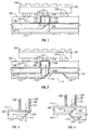
- Fig. 1 is a cross-sectional depiction of IC 101 mounted to PCB 102, showing optical via (OV) 109 and optical waveguide layer 106.
- IC 101 is mounted flip-chip style with heat sink 100 for cooling mounted on its upper surface.
- Conventional IC mounting pads 103 can be used in mounting IC 101 to PCB 102.
- An optical signal source or optoelectronic device (OED) 104 is mounted to the IC using mounting pads 112.
- One example of a suitable optical signal source 104 is a VCSEL.
- VCSEL VCSEL
- a VCSEL-to-OV gap 115 is designed into the tolerances so as to protect the VCSEL from possible damage during the assembly process.
- the VCSEL is configured to emit optical signal 110 into OV 109.
- An optical waveguide is formed within the OV hole of PCB 102 by appropriate means, such as by first coating the wall of OV 109 with a material 108 of one index of refraction (for example, a polymer). This first coating becomes the cladding of the OV waveguide. The remainder of OV 109 is then filled with an optical waveguide material, such as glass, with a slightly higher index of refraction than the cladding to form a core in order to ensure that light is guided through the core of OV 109.
- a segment of an optical waveguide, already having appropriate cladding may be installed in the hole in the PCB, rather than it being formed in place.
- Refractive index matching gel 111 is preferably sandwiched between PCB 102 and optical waveguide 106 in order to maintain proper transmission of optical signal 110.
- a 90-degree light reflection is achieved by preparing in or on the end of the waveguide a surface 105 at about a 45-degree angle to allow optical signal 110 to be redirected along waveguide 106.
- Angled reflective surface 105 may be prepared, for example, by cutting with laser ablation.
- a dielectric stack, beam splitter or micro-mirror, among others, may also be used to direct the optical signal.
- Waveguide cladding material 107 is shown used on the outside of waveguide 106.
- An air-gap A is shown at the opposite side of reflecting surface 105.
- second waveguide 113 having cladding 107 on both sides.
- a second waveguide may or may not be included in the structure, depending on circuit densities required.
- Fig. 1 shows a VCSEL
- an optical signal receiving device such as a photodetector could be mounted in much the same manner to IC 101.
- the photodetector would detect a light signal entering OV 109 from waveguide layer 106 that is directed 90-degrees from the waveguide into the OV.
- optical signal 110 would have a direction opposite from that shown in Fig. 1.
- Waveguide 106 may be positioned on PCB 102 by the use of conventional aligning registration elements, or locating marks (not shown), both in waveguide 106 and in PCB 102.
- Fig. 2 is a cross-sectional view, similar to Fig. 1, where a two-layer optical waveguide is depicted and the VCSEL is replaced with photodetector 114.
- First internal waveguide 106 and cladding 107 are shown along with a second waveguide 113 and outer cladding 107.
- Photodetector 114 acts to detect optical signal 110, which would be an input into IC 101.
- Precut waveguides 106 and 113 and their respective claddings 107 could be manufactured separately and assembled to each other and to the PCB, and alignment could be accomplished by use of appropriate registration elements (not shown).
- the input optical signal 110 is deflected by surface 116, which is at about a 45-degree angle, through waveguide hole H cut through the cladding and inner waveguide 106 and up to OV 109.
- Waveguide hole H is first coated by cladding material 108a, which is similar to material 108, and then filled with an optically transmissive epoxy or gel having a refractive index substantially matching that of OV 109.
- Waveguide 113 and outer cladding 107 could be continued at a further 45-degree cut point as long as a sufficient air-gap A separates 45-degree surface 116 below OV 109.
- Fig. 3 is an enlarged cross-sectional view depicting surface 105 at about 45-degrees functioning as a beam splitter which is sometimes referred to as a dielectric stack.
- Optical signal 110 passes through OV 109 and is then split by dielectric stack 105, which is located in waveguide 106. The optical signal is split into 90-degree offset optical signal 117 which passes along waveguide 106, and optical signal 118 that passes through dielectric stack 105.
- Optical signal 118 is then available for use, detection, or redirection, possibly by another waveguide or redirecting element (not shown). This technique could be used to allow an optical signal 110 to be sent to more than one photodetector location, for example.
- Fig. 4 is again an enlarged cross-sectional view of an OV depicting 45-degree surfaces 105 and 119, with upper surface 105 functioning as a dielectric stack or beam splitter.
- Upper dielectric stack surface 105 both passes through a portion of optical signal 110 and reflects the remainder of the optical signal 90-degrees to send optical signal 117 along waveguide 106.
- Second 45-degree surface 119 reflects the pass-through optical signal in a diametrically opposite 90-degree direction to send resultant signal 120 along another waveguide 121 which has cladding 126.
- original optical signal 110 is split into two optical signals 117, 120 for transmission in opposite directions for two separate purposes, such as to terminate at different respective photodetectors.
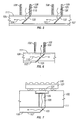
- Fig. 5 is another enlarged cross-sectional view showing two optical signals 110 and 126 reflected into one waveguide 106.
- Optical signal 126 may be originated by a VCSEL (not shown) and directed into OV 125. Another optical signal 110 passes through OV 109.
- First 45-degree surface 122 reflects optical signal 126 by 90-degrees to become resultant reflected optical signal 123 which passes into waveguide 106.
- Second 45-degree surface 105 incorporates a dielectric to reflect optical signal 110 into waveguide 106 and pass through optical signal 123.
- the resulting optical signal 124 is either optical signal 110 "OR" optical signal 123 or "Both".
- Fig. 5 thus depicts signals which perform a logical "OR” function. This could be accomplished if optical signals 110 and 126 have different wavelengths, for example.
- Fig. 6 is yet another enlarged cross-sectional view of an embodiment of the invention, where optical signal 110 is partially deflected into OV 109 and partially passed through angled surface 105 to continue along waveguide 106.
- Dielectric stack (beam splitter) 105 acts to split optical signal 110 into OV 109 and also passes a portion of the optical signal through to allow it to continue along waveguide 106.
- Fig. 7 shows a low profile configuration where the OED 131 is mounted to IC 101 which, in turn, has a heat sink upper surface 100.
- PCB 102 has OV 109 with cladding 108, waveguide 106, reflective angled surface 105, and refractive index matching gel 111.
- Other elements which may be included and are shown in previously-discussed figures, are omitted here for clarity.
- the only difference from Fig. 1 is that the PCB and the OV are countersunk so that the IC rests on mounting pads 103 on the top surface of the PCB, and OED 131 resides below the surface of the PCB.
- Fig. 8 depicts an alternative embodiment where optical fiber or waveguide 135 is coupled directly from an external signal source to OV 109. That signal could be reflected internally as in Fig. 1, or it could pass to another optical waveguide or fiber 136 on the other side of PCB 102.
- Fig. 9 shows another alternative embodiment of the invention, where optoelectronic devices 104 and 204 communicate directly through optical via 109.
- Integrated circuit 201 typically has heat sink 200 thereon, as previously described with respect to Fig. 1.
- the remaining reference numerals correspond to those in Fig. 1.
- one of OEDs 104, 204 may be a VCSEL and the other could be a photodetector. Other appropriate elements could also be used.
- An IC/OED source of an optical signal is shown and described as being mounted directly on the outer surface of a multi-layer PCB. That device could be an optical signal source such as a VCSEL, an optical signal receiving device such as a photodector, or any other source or receiver of an optical signal. Further, the optical signal device could be an optoelectronic transceiver, since elements 104, 204, 114, and 131 can function to emit or receive an optical signal. It is to be understood that any IC/OED that generates or receives an optical signal need not be mounted to the PCB.
- the optical signal may be coupled to the optical via directly by means of an optical waveguide, or through free space between the OED and the optical via, or by means of a combination thereof. It is contemplated that the various embodiments of the invention transmit, reflect, refract, and partially transmit, reflect or refract, optical signals from whatever source, on or remote from the PCB.
Landscapes
- Engineering & Computer Science (AREA)
- Physics & Mathematics (AREA)
- Electromagnetism (AREA)
- Computer Networks & Wireless Communication (AREA)
- Signal Processing (AREA)
- Microelectronics & Electronic Packaging (AREA)
- Optical Couplings Of Light Guides (AREA)
- Optical Integrated Circuits (AREA)
- Semiconductor Lasers (AREA)
Abstract
Description
- The present invention relates generally to optical communications through layers of printed circuit board (PCBs).
- Multi-layer PCBs are required due to the large number of electrical signals and the necessarily large number of signal paths. Limitations exist with this prior art technology with regard to how closely spaced electrical signal paths can be placed. Spacing limitations are a result of increasing signal speeds, potential metal migration problems (growth and shorting as a result of voltage differentials), and manufacturing specifications. Also, the length of a circuit from one device to another becomes a concern as circuit input/output speeds increase. Thus, device connection lengths become important concerns with limitations that are, at times, very difficult to overcome. The prior art also utilizes plating and etching processes which can be prone to manufacturing defects such as over-etching a circuit (potential open circuit or future open circuit) or under-etching, which has the potential to have a short circuit from one circuit to another (or future short). Systems which use electrical signals to transmit information from one chip to another on the same printed circuit board, or to another printed circuit board (PCB) with an electrical backplane, typically use multi-layer printed circuit boards in order to route the numerous signals on the PCB.
- Present day multi-layer PCBs are manufactured with both surface and multiple internal layers of circuit carriers, commonly referred to as inner-planes. Via holes, usually copper, are used to carry signals from one location to another through the surface and inner-plane circuit connections. Via holes are also used to connect surface mount devices to inner-planes. Circuit pads on the surface layers are used for surface mounted devices (SMDs) and larger via holes are used to connect devices with through-pins from the device to another signal layer in the same PCB. Internal via connections are also used to internally connect a signal from one inner-plane to another inner-plane.
- Making via holes with an electrically conductive lining is not suitable when optical signals are introduced to the surface of a multi-layer PCB that needs to be coupled through the PCB to another location, for example, to an internal optical waveguide.
- The present invention provides improvements over the prior art by utilizing optical waveguides in the form of an optical via to transmit signals through PCB layers rather than employing standard copper (or other metal) signal carriers. Various embodiments of the invention utilize optical carriers to route optical signals and to interconnect input/output devices within a PCB and alternatively route optical signals from one chip or integrated circuit (IC) to another in a multi-layer optical waveguide. Some embodiments of the invention employ optical vias to route optical signals through an otherwise electrical PCB to a multi-layer optical waveguide circuit.
- Although the embodiments of the invention are described with the use of optical signals, the concepts can include other energy forms such as microwave, for example.
- The objects, features and advantages of the invention will be more clearly perceived from the following detailed description, when read in conjunction with the accompanying drawing, in which:
- Fig. 1 is an enlarged cross-sectional view showing an integrated circuit / optoelectronic device with an optical via and an optical waveguide layer in accordance with an embodiment of the invention;
- Fig. 2 is a cross-sectional view, similar to Fig. 1, showing a two-layer optical waveguide, in accordance with an embodiment of the invention;
- Fig. 3 is a further enlarged cross-sectional view of an optical via, also depicting a dielectric stack or beam splitter, in accordance with an embodiment of the invention;
- Fig. 4 is another further enlarged cross-sectional view of an optical via depicting two dielectric stacks or beam splitters, in accordance with an embodiment of the invention;
- Fig. 5 is still another further enlarged cross-sectional view of two optical vias and two optical signals refracted into one waveguide, in accordance with an embodiment of the invention;
- Fig. 6 is yet another further enlarged cross sectional view of an optical signal deflected into an optical via and passed through a dielectric stack to continue along the waveguide, in accordance with an embodiment of the invention;
- Fig. 7 is a partial cross-sectional view, similar to Fig. 1, of an embodiment of the invention;
- Fig. 8 is another partial cross-sectional view of yet another embodiment of the invention; and
- Fig. 9 is a sectional view similar to Fig. 1, showing an optoelectronic device on either end of the optical via.
-
- Before explaining the disclosed embodiments of the present invention in detail, it is to be understood that the invention is not limited in its application to the details of the particular arrangements shown, since the invention is capable of other embodiments. Also, the terminology used herein is for the purpose of description and not of limitation.
- Generally the invention employs optical vias to pass optical signals through a PCB, such as from an optoelectronic device, such as a VCSEL, to another location for any desired purpose. For example, an embodiment of the invention utilizes optoelectronic devices (OEDs) mounted to, or remote from, integrated circuits to send and receive optical signals. A PCB can be configured for surface mounting of integrated circuits providing voltage and mechanical connection pads along with optical via-hole connections.
- In some embodiments, the present invention utilizes optical waveguides or carriers to route optical signals from one location to another. According to one embodiment, once an optical signal has been generated, such as by an OED, the optical signal is routed from the top surface of and through the PCB to an attached optical waveguide carrier. The connection from the top surface to the optical waveguide is through an optical via. The optical via (OV) is a hole in the PCB that is filled with an optical waveguide to route the light signal (emitted or received) through the PCB. The attached waveguide then optically routes the signal to other appropriate locations. The optical signal can be routed to an optoelectronic device, such as a photodetector, at a predetermined location on the PCB, or elsewhere if desired, through another OV. Any OED employed could be flip chipped to an IC which could be configured with a conventional heat sink.
- An OED can be a vertical-cavity surface-emitting laser (VCSEL) or a photodetector that could be mounted in a "flip-chip" style onto an IC device such that optical signals are emitted perpendicular to the IC and thus perpendicular to the PCB. In such an arrangement, the IC/OED is mounted onto the PCB (onto an electrical pad layout) at a predetermined position relative to the IC electrical pads. The IC still has surface mounting pads for voltage, and ground, for example. The relationship between the IC pads and the OED(s) could well be specified for manufacturing mounting requirements. Thus, in this case, the VCSEL would be a bottom-emitting device, and a detector at a different location would be a bottom-receiving or bottom-illuminated device. The IC/OED would be mounted in position over the OV. Optoelectronic devices in combination with the appropriate ICs which both emit and receive optical signals (transceivers) are also within the scope of this invention.
- An optical waveguide can be formed, as an example, within the hole of the PCB by first coating the walls of the OV hole with a material of one index of refraction (for example, a polymer). This first coating becomes the cladding of the OV waveguide. The remainder of the OV is then filled with a material with a slightly different (higher) index of refraction to form the optical waveguide core in the OV. This structure provides that light beams or signals are guided through the core of the OV in an efficient, effective and positive manner. Other ways to form the desired optical characteristics in the OV may be employed. It is possible that a core and cladding unit could be preformed and inserted into the appropriate hole in the PCB.
- A refractive index matching fluid should be used between the bottom of the PCB and the top of the attached waveguide. A thin layer of such material would be sandwiched between the transmission portion of the optical waveguide and the bottom of the PCB in order to maintain guiding of light from the OV to the optical waveguide. Finally, the outer layer of the optical waveguide layer would typically consist of a cladding material.
- An embodiment of the present invention contemplates an optical waveguide (optical via) completely through a PCB so that an optical signal from any source external to the PCB can be transmitted through the PCB to be received or further transmitted by any suitable means on or from the opposite side of the PCB.
- Another embodiment of the invention incorporates an OV partially through the PCB from one surface to an internal optical waveguide which is typically arranged parallel to the PCB surface. That waveguide can be employed to transmit the optical signal from one OV to another OV, or to a location at the edge of the PCB for coupling to another device or to another PCB or backplane.
- A multi-layer optical waveguide can be used where the quantity of optical circuits are such as to need an increase in density. By using multi-layer waveguides, optical signals can be split into "x" and "y" plane channels.
- Advanced levels of VCSEL controls allow for polarization controls such that a dielectric stack can pass one polarization in one direction along a waveguide and pass another polarization along another direction. Also, tunable VCSEL controls that can change the optical signal wavelength (under control) can accomplish sending an optical signal in one direction versus another direction along a waveguide by using a dielectric stack that passes one wavelength and reflects another.
- With reference now to the drawing, Fig. 1 is a cross-sectional depiction of
IC 101 mounted toPCB 102, showing optical via (OV) 109 andoptical waveguide layer 106.IC 101 is mounted flip-chip style withheat sink 100 for cooling mounted on its upper surface. ConventionalIC mounting pads 103 can be used in mountingIC 101 toPCB 102. An optical signal source or optoelectronic device (OED) 104, for example (only one is shown), is mounted to the IC using mountingpads 112. One example of a suitableoptical signal source 104 is a VCSEL. There could be many others and the term "VCSEL" will be used herein for simplicity. A VCSEL-to-OV gap 115 is designed into the tolerances so as to protect the VCSEL from possible damage during the assembly process. The VCSEL is configured to emitoptical signal 110 intoOV 109. - An optical waveguide is formed within the OV hole of
PCB 102 by appropriate means, such as by first coating the wall ofOV 109 with amaterial 108 of one index of refraction (for example, a polymer). This first coating becomes the cladding of the OV waveguide. The remainder ofOV 109 is then filled with an optical waveguide material, such as glass, with a slightly higher index of refraction than the cladding to form a core in order to ensure that light is guided through the core ofOV 109. Optionally, a segment of an optical waveguide, already having appropriate cladding, may be installed in the hole in the PCB, rather than it being formed in place. Refractiveindex matching gel 111 is preferably sandwiched betweenPCB 102 andoptical waveguide 106 in order to maintain proper transmission ofoptical signal 110. - A 90-degree light reflection is achieved by preparing in or on the end of the waveguide a
surface 105 at about a 45-degree angle to allowoptical signal 110 to be redirected alongwaveguide 106. Angledreflective surface 105 may be prepared, for example, by cutting with laser ablation. A dielectric stack, beam splitter or micro-mirror, among others, may also be used to direct the optical signal.Waveguide cladding material 107 is shown used on the outside ofwaveguide 106. An air-gap A is shown at the opposite side of reflectingsurface 105. Also shown issecond waveguide 113 havingcladding 107 on both sides. A second waveguide may or may not be included in the structure, depending on circuit densities required. - Note that although Fig. 1 shows a VCSEL, an optical signal receiving device such as a photodetector could be mounted in much the same manner to
IC 101. The photodetector would detect a lightsignal entering OV 109 fromwaveguide layer 106 that is directed 90-degrees from the waveguide into the OV. Thus,optical signal 110 would have a direction opposite from that shown in Fig. 1.Waveguide 106 may be positioned onPCB 102 by the use of conventional aligning registration elements, or locating marks (not shown), both inwaveguide 106 and inPCB 102. - Fig. 2 is a cross-sectional view, similar to Fig. 1, where a two-layer optical waveguide is depicted and the VCSEL is replaced with
photodetector 114. Firstinternal waveguide 106 andcladding 107 are shown along with asecond waveguide 113 andouter cladding 107.Photodetector 114 acts to detectoptical signal 110, which would be an input intoIC 101.Precut waveguides respective claddings 107 could be manufactured separately and assembled to each other and to the PCB, and alignment could be accomplished by use of appropriate registration elements (not shown). The inputoptical signal 110 is deflected bysurface 116, which is at about a 45-degree angle, through waveguide hole H cut through the cladding andinner waveguide 106 and up toOV 109. Waveguide hole H is first coated by cladding material 108a, which is similar tomaterial 108, and then filled with an optically transmissive epoxy or gel having a refractive index substantially matching that ofOV 109.Waveguide 113 andouter cladding 107 could be continued at a further 45-degree cut point as long as a sufficient air-gap A separates 45-degree surface 116 belowOV 109. - Fig. 3 is an enlarged cross-sectional
view depicting surface 105 at about 45-degrees functioning as a beam splitter which is sometimes referred to as a dielectric stack.Optical signal 110 passes throughOV 109 and is then split bydielectric stack 105, which is located inwaveguide 106. The optical signal is split into 90-degree offsetoptical signal 117 which passes alongwaveguide 106, andoptical signal 118 that passes throughdielectric stack 105.Optical signal 118 is then available for use, detection, or redirection, possibly by another waveguide or redirecting element (not shown). This technique could be used to allow anoptical signal 110 to be sent to more than one photodetector location, for example. - Fig. 4 is again an enlarged cross-sectional view of an OV depicting 45-
degree surfaces upper surface 105 functioning as a dielectric stack or beam splitter. Upperdielectric stack surface 105 both passes through a portion ofoptical signal 110 and reflects the remainder of the optical signal 90-degrees to sendoptical signal 117 alongwaveguide 106. Second 45-degree surface 119 reflects the pass-through optical signal in a diametrically opposite 90-degree direction to sendresultant signal 120 along anotherwaveguide 121 which hascladding 126. In this manner, originaloptical signal 110 is split into twooptical signals - Fig. 5 is another enlarged cross-sectional view showing two
optical signals waveguide 106.Optical signal 126 may be originated by a VCSEL (not shown) and directed intoOV 125. Anotheroptical signal 110 passes throughOV 109. First 45-degree surface 122 reflectsoptical signal 126 by 90-degrees to become resultant reflectedoptical signal 123 which passes intowaveguide 106. Second 45-degree surface 105 incorporates a dielectric to reflectoptical signal 110 intowaveguide 106 and pass throughoptical signal 123. The resultingoptical signal 124 is eitheroptical signal 110 "OR"optical signal 123 or "Both". Fig. 5 thus depicts signals which perform a logical "OR" function. This could be accomplished ifoptical signals - Fig. 6 is yet another enlarged cross-sectional view of an embodiment of the invention, where
optical signal 110 is partially deflected intoOV 109 and partially passed through angledsurface 105 to continue alongwaveguide 106. Dielectric stack (beam splitter) 105 acts to splitoptical signal 110 intoOV 109 and also passes a portion of the optical signal through to allow it to continue alongwaveguide 106. - Fig. 7 shows a low profile configuration where the
OED 131 is mounted toIC 101 which, in turn, has a heat sinkupper surface 100.PCB 102 hasOV 109 withcladding 108,waveguide 106, reflectiveangled surface 105, and refractiveindex matching gel 111. Other elements which may be included and are shown in previously-discussed figures, are omitted here for clarity. The only difference from Fig. 1 is that the PCB and the OV are countersunk so that the IC rests on mountingpads 103 on the top surface of the PCB, andOED 131 resides below the surface of the PCB. - Fig. 8 depicts an alternative embodiment where optical fiber or
waveguide 135 is coupled directly from an external signal source toOV 109. That signal could be reflected internally as in Fig. 1, or it could pass to another optical waveguide orfiber 136 on the other side ofPCB 102. - Fig. 9 shows another alternative embodiment of the invention, where
optoelectronic devices Integrated circuit 201 typically hasheat sink 200 thereon, as previously described with respect to Fig. 1. The remaining reference numerals correspond to those in Fig. 1. In this embodiment one ofOEDs - Although a 45-degree angle has been depicted in the embodiments shown in the figures, different angles may be employed in alternative embodiments, depending on specific requirements. An IC/OED source of an optical signal is shown and described as being mounted directly on the outer surface of a multi-layer PCB. That device could be an optical signal source such as a VCSEL, an optical signal receiving device such as a photodector, or any other source or receiver of an optical signal. Further, the optical signal device could be an optoelectronic transceiver, since
elements - Although the present invention has been described with reference to preferred embodiments, numerous modifications and variations can be made and still the result will come within the scope of the invention. No limitation with respect to the specific embodiments disclosed herein is intended or should be inferred. The invention is defined by the appended claims and their equivalents.
Claims (19)
- A printed circuit board (PCB) comprising:a substrate (102);a mounting surface on said substrate;a hole starting at said mounting surface and extending through said substrate to an exit port;a cladding material (108) lining said hole; andan optical waveguide core within said lining, said core having an index of refraction higher than said cladding, thereby forming an optical via (109) capable of transmitting an optical signal through said hole.
- The printed circuit board of claim 1, further comprising an optical waveguide (106) spaced from and parallel with said mounting surface of said substrate.
- The printed circuit board of claim 2, wherein said optical waveguide further comprises an angled surface (105) adjacent said exit port of said hole, thereby redirecting the optical signal and allowing at least a portion of the transmitted optical signal to pass through said hole and into said optical waveguide.
- The printed circuit board of one of claims 1 to 3, further comprising a first optoelectronic device (104) on said mounting surface, said optoelectronic device being configured to transmit or receive an optical signal through said optical via.
- The printed circuit board of claim 4, further comprising a second optoelectronic device (204), said first and second optoelectronic devices selectively communicating optical signals through said optical via.
- The printed circuit board of claim 3, wherein said angled surface comprises a dielectric stack, thereby reflecting some wavelengths of light and passing other wavelengths of light impinging on it.
- The printed circuit board of one of claims 1 to 6, further comprising a first optical waveguide means (135) coupled to one end of said optical via for conveying an optical signal to or away from said optical via.
- The printed circuit board of claim 7, further comprising a second optical waveguide means (136) coupled to the opposite end of said optical via for conveying the optical signal away or to said optical via in cooperation with said first optical waveguide.
- The printed circuit board of claim 4, further comprising an integrated circuit (IC) (101), said optoelectronic device being mounted onto one side of said IC, said IC being mounted to said mounting surface.
- A printed circuit board (PCB) comprising:substrate means (102) configured with a mounting surface;an optoelectronic device (104) mounted on said mounting surface for providing an optical signal;optical waveguide means (106) coupled to said substrate means spaced from and substantially parallel with said mounting surface; andvia hole means through said substrate means and functioning as an optical waveguide (109) to transmit optical signals therethrough from said optoelectronic device to said optical waveguide means.
- The printed circuit board of claim 10, wherein said waveguide means further comprises means (105) to at least partially redirect the optical signal from said via hole means along said waveguide means (106).
- Apparatus for providing communication of signals through layers in a printed circuit board (PCB) having a substrate with a first surface, the apparatus comprising:a first electronic component (104) selectively configured to generate a signal, receive a signal, or function as a signal transceiver;a first via hole formed in said substrate;a first waveguide (109) in said first via hole to facilitate transmission of a signal therethrough from an input end to an exit end of said first via hole;means for coupling a signal through said via hole to or away from said first electronic component;a second waveguide (107) mounted adjacent to said exit end of said first via hole; anda first angled surface (116) in said second waveguide, said angled surface being positioned to selectively redirect at least a portion of a signal into and out of said first via hole, thereby enabling said first electronic component to send a signal to or receive a signal from another location through said second waveguide.
- The apparatus of claim 12, wherein the signal is an optical signal, said first electronic component is an optoelectronic device, said first waveguide is an optical waveguide forming a first optical via, and said second waveguide is an optical waveguide.
- The apparatus of claim 13, further comprising a third optical waveguide (113) substantially parallel to said second optical waveguide.
- The apparatus of claim 13 or 14, further comprising at least one second via hole (125) comprising a second optical via, said second optical via being spaced from said first optical via through which optical signals are transmitted.
- The apparatus of claim 12, wherein said first electronic component is selected from the group consisting of a vertical-cavity surface-emitting laser (VCSEL), an optical signal receiving device, and an optoelectronic transceiver.
- A method for communicating optical signals through layers in a printed circuit board (PCB) having a substrate (102) with a first surface and a second surface spaced from and substantially parallel with said first surface, the method comprising:forming a hole through the PCB;installing an optical waveguide (106) in the hole to form an optical via (109) through the printed circuit board;coupling an optical signal from an optical signal source to said optical via; andpassing the optical signal through the optical via.
- The method of claim 17, wherein installing the optical waveguide in the hole is accomplished by coating the wall of the hole with a cladding material (108) and then filling the remainder of the hole with an optical waveguide material.
- The method of claim 17, wherein installing the optical waveguide in the hole is accomplished by fitting a segment of an optical waveguide (106), including its own cladding (108), in the hole.
Applications Claiming Priority (2)
| Application Number | Priority Date | Filing Date | Title |
|---|---|---|---|
| US10/365,127 US7263248B2 (en) | 2003-02-11 | 2003-02-11 | Optical via to pass signals through a printed circuit board |
| US365127 | 2003-02-11 |
Publications (2)
| Publication Number | Publication Date |
|---|---|
| EP1447694A1 true EP1447694A1 (en) | 2004-08-18 |
| EP1447694B1 EP1447694B1 (en) | 2008-05-07 |
Family
ID=32681703
Family Applications (1)
| Application Number | Title | Priority Date | Filing Date |
|---|---|---|---|
| EP03021693A Expired - Lifetime EP1447694B1 (en) | 2003-02-11 | 2003-09-29 | Optical via for transmission of signals through a printed circuit board |
Country Status (3)
| Country | Link |
|---|---|
| US (2) | US7263248B2 (en) |
| EP (1) | EP1447694B1 (en) |
| DE (1) | DE60320744D1 (en) |
Cited By (6)
| Publication number | Priority date | Publication date | Assignee | Title |
|---|---|---|---|---|
| WO2006032726A1 (en) * | 2004-09-23 | 2006-03-30 | Aspocomp Technology Oy | Method for assembling an opto-electric module and a structure of an opto-electric module |
| EP1720048A1 (en) | 2005-05-03 | 2006-11-08 | Delphi Technologies, Inc. | Illuminated display system |
| EP1930755A4 (en) * | 2005-09-30 | 2009-10-28 | Mitsumi Electric Co Ltd | Optical waveguide device and method for fabricating optical waveguide device |
| WO2011019435A3 (en) * | 2009-05-27 | 2011-04-21 | University Of Delaware | Formation of reflective surfaces in printed circuit board waveguides |
| EP2128674A3 (en) * | 2008-05-27 | 2014-01-15 | Nitto Denko Corporation | Opto-electric hybrid module and manufacturing method thereof |
| EP2613188A4 (en) * | 2010-08-31 | 2018-01-17 | Kyocera Corporation | Optical transmission substrate, optical transmission module, and method for manufacturing optical transmission substrate |
Families Citing this family (69)
| Publication number | Priority date | Publication date | Assignee | Title |
|---|---|---|---|---|
| CA2504222C (en) | 2002-10-22 | 2012-05-22 | Jason A. Sullivan | Robust customizable computer processing system |
| CA2503793A1 (en) | 2002-10-22 | 2004-05-06 | Jason A. Sullivan | Systems and methods for providing a dynamically modular processing unit |
| EP1557075A4 (en) | 2002-10-22 | 2010-01-13 | Sullivan Jason | Non-peripherals processing control module having improved heat dissipating properties |
| US7263248B2 (en) * | 2003-02-11 | 2007-08-28 | Avago Technologies Fiber Ip (Singapore) Pte. Ltd. | Optical via to pass signals through a printed circuit board |
| US7391937B2 (en) * | 2004-10-22 | 2008-06-24 | Lockheed Martin Corporation | Compact transition in layered optical fiber |
| US7500792B2 (en) * | 2004-11-26 | 2009-03-10 | Finisar Corporation | Optoelectronic transmitting and/or receiving arrangement |
| US7551811B2 (en) * | 2005-01-19 | 2009-06-23 | Bridgestone Corporation | Optical device and method for producing the same |
| CN101501543B (en) * | 2006-06-30 | 2013-04-17 | 应用材料公司 | Wafer-level alignment of optical elements |
| KR100871252B1 (en) * | 2007-01-19 | 2008-11-28 | 삼성전자주식회사 | Flexible printed circuit board with optical / electrical wiring using optical fiber |
| US8265432B2 (en) * | 2008-03-10 | 2012-09-11 | International Business Machines Corporation | Optical transceiver module with optical windows |
| WO2009119850A1 (en) * | 2008-03-27 | 2009-10-01 | 京セラ株式会社 | Composite optical transmission substrate and optical module |
| US7486847B1 (en) | 2008-03-31 | 2009-02-03 | International Business Machines Corporation | Chip carrier package with optical vias |
| US7672560B2 (en) * | 2008-05-13 | 2010-03-02 | International Business Machines Corporation | Coupling device for use in optical waveguides |
| KR100969435B1 (en) * | 2008-05-23 | 2010-07-14 | 삼성전기주식회사 | Printed circuit board having optical waveguide and manufacturing method thereof |
| US7802927B2 (en) * | 2008-05-30 | 2010-09-28 | Corning Cable Systems Llc | Bent optical fiber couplers and opto-electrical assemblies formed therefrom |
| US8171625B1 (en) | 2008-06-02 | 2012-05-08 | Wavefront Research, Inc. | Method of providing low footprint optical interconnect |
| KR101246137B1 (en) * | 2008-12-19 | 2013-03-25 | 한국전자통신연구원 | Light emitting device and optical coupling module |
| US9057853B2 (en) * | 2009-02-20 | 2015-06-16 | The Hong Kong University Of Science And Technology | Apparatus having an embedded 3D hybrid integration for optoelectronic interconnects |
| US8604603B2 (en) * | 2009-02-20 | 2013-12-10 | The Hong Kong University Of Science And Technology | Apparatus having thermal-enhanced and cost-effective 3D IC integration structure with through silicon via interposers |
| US8593826B2 (en) * | 2009-09-18 | 2013-11-26 | Samsung Electronics Co., Ltd. | Memory module, memory system having the memory module, and method for manufacturing the memory module |
| US8867871B2 (en) | 2009-10-08 | 2014-10-21 | Lg Innotek Co., Ltd. | Optical printed circuit board and method of fabricating the same |
| KR20110039017A (en) * | 2009-10-09 | 2011-04-15 | 엘지이노텍 주식회사 | Optical Printed Circuit Board and Manufacturing Method Thereof |
| JP5493744B2 (en) * | 2009-11-12 | 2014-05-14 | 富士通株式会社 | Opto-electric hybrid board and method for manufacturing opto-electric hybrid board |
| US20110243509A1 (en) * | 2010-04-05 | 2011-10-06 | Avago Technologies Fiber Ip (Singapore) Pte. Ltd. | Opto-electronic transceiver module system |
| US8632261B2 (en) * | 2010-04-20 | 2014-01-21 | Hon Hai Precision Industry Co., Ltd. | Integrated and sealed opto-electronic device assembly |
| US8399292B2 (en) * | 2010-06-30 | 2013-03-19 | International Business Machines Corporation | Fabricating a semiconductor chip with backside optical vias |
| JP5505140B2 (en) * | 2010-07-05 | 2014-05-28 | 富士通株式会社 | Optical module and manufacturing method |
| EP2613187B1 (en) * | 2010-08-31 | 2019-05-08 | Kyocera Corporation | Optical transmission body, method for producing same, and optical transmission module |
| US8680458B2 (en) | 2010-10-07 | 2014-03-25 | Empire Technology Development, Llc | Data transmission through optical vias |
| WO2012069929A1 (en) * | 2010-11-25 | 2012-05-31 | Fci | Optical circuit board |
| WO2012096651A1 (en) * | 2011-01-11 | 2012-07-19 | Hewlett-Packard Development Company, L.P. | Passive optical alignment |
| US8708576B2 (en) * | 2011-01-20 | 2014-04-29 | Harris Corporation | Electro-optical device having an elastomeric body and related methods |
| WO2012109393A1 (en) | 2011-02-08 | 2012-08-16 | Henry Cooper | High gain frequency step horn antenna |
| WO2012109498A1 (en) | 2011-02-09 | 2012-08-16 | Henry Cooper | Corrugated horn antenna with enhanced frequency range |
| JP2012194401A (en) * | 2011-03-16 | 2012-10-11 | Nitto Denko Corp | Opto-electric hybrid substrate and manufacturing method of the same |
| US8818145B2 (en) * | 2011-08-03 | 2014-08-26 | Tyco Electronics Corporation | Optical interposer with transparent substrate |
| US9570420B2 (en) * | 2011-09-29 | 2017-02-14 | Broadcom Corporation | Wireless communicating among vertically arranged integrated circuits (ICs) in a semiconductor package |
| US9318785B2 (en) | 2011-09-29 | 2016-04-19 | Broadcom Corporation | Apparatus for reconfiguring an integrated waveguide |
| US8855452B2 (en) | 2012-01-18 | 2014-10-07 | International Business Machines Corporation | Silicon photonic chip optical coupling structures |
| KR20140120885A (en) | 2012-01-31 | 2014-10-14 | 휴렛-팩커드 디벨롭먼트 컴퍼니, 엘.피. | Combination underfill-dam and electrical-interconnect structure for an opto-electronic engine |
| CN104246564B (en) | 2012-04-25 | 2016-03-02 | 惠普发展公司,有限责任合伙企业 | Electricity/optical conenctor |
| TWI561881B (en) * | 2012-04-27 | 2016-12-11 | Hon Hai Prec Ind Co Ltd | Fiber optical transceiver |
| JP6001327B2 (en) * | 2012-05-23 | 2016-10-05 | 京セラ株式会社 | Optical wiring component, optical wiring module, and optical wiring device |
| US9323014B2 (en) * | 2012-05-28 | 2016-04-26 | Mellanox Technologies Ltd. | High-speed optical module with flexible printed circuit board |
| JP6081086B2 (en) * | 2012-06-14 | 2017-02-15 | Tdk株式会社 | Mounting device and mounting method for photoelectric element |
| US9195007B2 (en) * | 2012-06-28 | 2015-11-24 | Intel Corporation | Inverted 45 degree mirror for photonic integrated circuits |
| US9172462B2 (en) * | 2012-12-31 | 2015-10-27 | Zephyr Photonics Inc. | Optical bench apparatus having integrated monitor photodetectors and method for monitoring optical power using same |
| US9761746B2 (en) | 2013-03-11 | 2017-09-12 | Intel Corporation | Low voltage avalanche photodiode with re-entrant mirror for silicon based photonic integrated circuits |
| US9450309B2 (en) | 2013-05-30 | 2016-09-20 | Xi3 | Lobe antenna |
| US9804348B2 (en) | 2013-07-04 | 2017-10-31 | Mellanox Technologies, Ltd. | Silicon photonics connector |
| US9454177B2 (en) * | 2014-02-14 | 2016-09-27 | Apple Inc. | Electronic devices with housing-based interconnects and coupling structures |
| WO2016007958A2 (en) * | 2014-07-11 | 2016-01-14 | Xi3, Inc. | Systems and methods for providing a high power pc board air dielectric splitter |
| US10209464B2 (en) * | 2014-10-17 | 2019-02-19 | Cisco Technology, Inc. | Direct printed circuit routing to stacked opto-electrical IC packages |
| US9543463B2 (en) | 2014-10-27 | 2017-01-10 | International Business Machines Corporation | Signal distribution in integrated circuit using optical through silicon via |
| KR102429868B1 (en) | 2014-12-04 | 2022-08-05 | 삼성전자주식회사 | Llight interconnection device using a plasmonic via |
| KR102349774B1 (en) * | 2015-03-11 | 2022-01-10 | 삼성전자주식회사 | Photonic Integrated Circuit |
| EP3345030B1 (en) * | 2015-09-03 | 2019-07-24 | Telefonaktiebolaget LM Ericsson (publ) | System, method, and apparatus for optical broadcast transmission in a circuit board |
| US9709748B2 (en) * | 2015-09-03 | 2017-07-18 | International Business Machines Corporation | Frontside coupled waveguide with backside optical connection using a curved spacer |
| US9759634B2 (en) | 2015-09-14 | 2017-09-12 | Seagate Technology Llc | Coupling loss evaluation |
| US10996401B2 (en) * | 2016-06-30 | 2021-05-04 | Mellanox Technologies, Ltd. | Method and apparatus for optical coupling of optical signals for a photonic integrated circuit |
| US10025044B1 (en) * | 2017-01-17 | 2018-07-17 | International Business Machines Corporation | Optical structure |
| US10168495B1 (en) * | 2017-06-28 | 2019-01-01 | Kyocera Corporation | Optical waveguide and optical circuit board |
| US10681832B1 (en) * | 2019-06-06 | 2020-06-09 | Hewlett Packard Enterprise Development Lp | High-density universally-configurable system board architecture with dual-use modular mid-board optics (MBOs) |
| WO2022149051A1 (en) * | 2021-01-07 | 2022-07-14 | Rockley Photonics Limited | Optical assemblies comprising a prism |
| US12085769B2 (en) * | 2021-04-23 | 2024-09-10 | Taiwan Semiconductor Manufacturing Company, Ltd. | Integrated circuit device and method |
| US12313890B2 (en) * | 2021-06-16 | 2025-05-27 | Intel Corporation | Through-substrate optical vias |
| US11867956B2 (en) * | 2021-08-19 | 2024-01-09 | Advanced Semiconductor Engineering, Inc. | Optoelectronic device |
| US12253727B2 (en) * | 2022-04-01 | 2025-03-18 | Unimicron Technology Corp. | Electronic device |
| TWI831270B (en) * | 2022-04-01 | 2024-02-01 | 欣興電子股份有限公司 | Electronic device |
Citations (2)
| Publication number | Priority date | Publication date | Assignee | Title |
|---|---|---|---|---|
| EP0986197A2 (en) * | 1998-09-07 | 2000-03-15 | Sony Corporation | Optical transmitting/receiving method and apparatus |
| WO2002050592A2 (en) * | 2000-12-19 | 2002-06-27 | Intel Corporation | Photonic and electronic components on a shared substrate with through substrate communication |
Family Cites Families (17)
| Publication number | Priority date | Publication date | Assignee | Title |
|---|---|---|---|---|
| US4732446A (en) * | 1985-10-02 | 1988-03-22 | Lamar Gipson | Electrical circuit and optical data buss |
| US4897711A (en) * | 1988-03-03 | 1990-01-30 | American Telephone And Telegraph Company | Subassembly for optoelectronic devices |
| JP2921877B2 (en) * | 1989-09-19 | 1999-07-19 | 富士通株式会社 | Waveguide demultiplexing module and method of manufacturing the same |
| JPH11183749A (en) * | 1997-12-22 | 1999-07-09 | Hitachi Chem Co Ltd | Optical circuit board and manufacture therefor |
| JP3715425B2 (en) * | 1998-03-06 | 2005-11-09 | ブラザー工業株式会社 | Manufacturing method of substrate with optical waveguide |
| US6785447B2 (en) * | 1998-10-09 | 2004-08-31 | Fujitsu Limited | Single and multilayer waveguides and fabrication process |
| TW451084B (en) * | 1999-06-25 | 2001-08-21 | Toppan Printing Co Ltd | Optical-electro wiring board, mounted board, and manufacturing method of optical-electro wiring board |
| JP3728147B2 (en) * | 1999-07-16 | 2005-12-21 | キヤノン株式会社 | Opto-electric hybrid wiring board |
| DE10032796A1 (en) * | 2000-06-28 | 2002-01-17 | Infineon Technologies Ag | optomodule |
| US6424761B1 (en) | 2001-01-22 | 2002-07-23 | Tycom (Us) Inc. | Cable repeater connecting joint |
| JP2002258081A (en) * | 2001-02-28 | 2002-09-11 | Fujitsu Ltd | Optical wiring board, method for manufacturing optical wiring board, and multilayer optical wiring |
| US6754407B2 (en) * | 2001-06-26 | 2004-06-22 | Intel Corporation | Flip-chip package integrating optical and electrical devices and coupling to a waveguide on a board |
| US6512861B2 (en) * | 2001-06-26 | 2003-01-28 | Intel Corporation | Packaging and assembly method for optical coupling |
| US6944377B2 (en) * | 2002-03-15 | 2005-09-13 | Hitachi Maxell, Ltd. | Optical communication device and laminated optical communication module |
| US20040042705A1 (en) * | 2002-08-27 | 2004-03-04 | Uchida Toshi K. | Embedded optical coupling in circuit boards |
| US7263248B2 (en) * | 2003-02-11 | 2007-08-28 | Avago Technologies Fiber Ip (Singapore) Pte. Ltd. | Optical via to pass signals through a printed circuit board |
| KR20050040589A (en) * | 2003-10-29 | 2005-05-03 | 삼성전기주식회사 | Painted circuit board having the waveguide and manufacturing method thereof |
-
2003
- 2003-02-11 US US10/365,127 patent/US7263248B2/en not_active Expired - Lifetime
- 2003-09-29 EP EP03021693A patent/EP1447694B1/en not_active Expired - Lifetime
- 2003-09-29 DE DE60320744T patent/DE60320744D1/en not_active Expired - Lifetime
-
2007
- 2007-07-17 US US11/779,116 patent/US7466880B2/en not_active Expired - Fee Related
Patent Citations (2)
| Publication number | Priority date | Publication date | Assignee | Title |
|---|---|---|---|---|
| EP0986197A2 (en) * | 1998-09-07 | 2000-03-15 | Sony Corporation | Optical transmitting/receiving method and apparatus |
| WO2002050592A2 (en) * | 2000-12-19 | 2002-06-27 | Intel Corporation | Photonic and electronic components on a shared substrate with through substrate communication |
Cited By (7)
| Publication number | Priority date | Publication date | Assignee | Title |
|---|---|---|---|---|
| WO2006032726A1 (en) * | 2004-09-23 | 2006-03-30 | Aspocomp Technology Oy | Method for assembling an opto-electric module and a structure of an opto-electric module |
| EP1720048A1 (en) | 2005-05-03 | 2006-11-08 | Delphi Technologies, Inc. | Illuminated display system |
| US7350934B2 (en) | 2005-05-03 | 2008-04-01 | Delphi Technologies, Inc. | Illuminated display system |
| EP1930755A4 (en) * | 2005-09-30 | 2009-10-28 | Mitsumi Electric Co Ltd | Optical waveguide device and method for fabricating optical waveguide device |
| EP2128674A3 (en) * | 2008-05-27 | 2014-01-15 | Nitto Denko Corporation | Opto-electric hybrid module and manufacturing method thereof |
| WO2011019435A3 (en) * | 2009-05-27 | 2011-04-21 | University Of Delaware | Formation of reflective surfaces in printed circuit board waveguides |
| EP2613188A4 (en) * | 2010-08-31 | 2018-01-17 | Kyocera Corporation | Optical transmission substrate, optical transmission module, and method for manufacturing optical transmission substrate |
Also Published As
| Publication number | Publication date |
|---|---|
| US20040156576A1 (en) | 2004-08-12 |
| DE60320744D1 (en) | 2008-06-19 |
| US7466880B2 (en) | 2008-12-16 |
| EP1447694B1 (en) | 2008-05-07 |
| US7263248B2 (en) | 2007-08-28 |
| US20070258676A1 (en) | 2007-11-08 |
Similar Documents
| Publication | Publication Date | Title |
|---|---|---|
| EP1447694B1 (en) | Optical via for transmission of signals through a printed circuit board | |
| US7242823B2 (en) | Optical transmission channel board, board with built-in optical transmission channel, and data processing apparatus | |
| KR100623477B1 (en) | Optical printed circuit board and optical connection block using optical fiber bundle | |
| US7724988B2 (en) | Opto-electronic board | |
| JP4457545B2 (en) | OPTICAL / ELECTRIC WIRING BOARD, MOUNTING BOARD, AND OPTOELECTRIC WIRING BOARD MANUFACTURING METHOD | |
| US7406229B2 (en) | Optical module | |
| KR100499005B1 (en) | A printed circuit board being packaged optical devices of multi-channel block type | |
| JP2000171671A (en) | Optical communication module and mounting method thereof | |
| CN101452096A (en) | Optical interconnection device | |
| JP2002006161A (en) | Optical wiring board, optical wiring module, and manufacturing method thereof | |
| US6408121B1 (en) | Optical communication module | |
| CN114127601B (en) | Optical circuit board and electronic component mounting structure using the same | |
| JP5078442B2 (en) | OPTICAL TRANSMISSION BOARD, MANUFACTURING METHOD THEREOF, OPTICAL ELECTRONIC HYBRID SUBSTRATE, AND OPTICAL MODULE | |
| JP2010028006A (en) | Optical device | |
| JP2006284781A (en) | Circuit board | |
| KR100821289B1 (en) | Flexible Optical Circuit Board and Manufacturing Method Thereof | |
| KR101664478B1 (en) | Optical module, optical printed circuit board and method for manufacturing the same | |
| JP2003227951A (en) | Optical waveguide device, manufacturing method thereof, and opto-electric hybrid board using the same | |
| KR100734906B1 (en) | Optical interconnect using flexible optical printed circuit board | |
| KR20010041501A (en) | Testing of optical transmitter and receiver modules | |
| KR100525223B1 (en) | An optical printed circuit board for transmitting of signals long-distance | |
| JP2005234557A (en) | Optical transmission path substrate manufacturing method, optical transmission path substrate, optical transmission path built-in substrate, optical transmission path built-in substrate manufacturing method, and data processing apparatus | |
| WO2008121075A1 (en) | Optical interconnect structure and method | |
| KR20040106674A (en) | Structures of optical waveguide laminated printed circuit board and optical connection blocks and method for constructing waveguide layer | |
| JP2001044552A (en) | Bidirectional optical module |
Legal Events
| Date | Code | Title | Description |
|---|---|---|---|
| PUAI | Public reference made under article 153(3) epc to a published international application that has entered the european phase |
Free format text: ORIGINAL CODE: 0009012 |
|
| AK | Designated contracting states |
Kind code of ref document: A1 Designated state(s): AT BE BG CH CY CZ DE DK EE ES FI FR GB GR HU IE IT LI LU MC NL PT RO SE SI SK TR |
|
| AX | Request for extension of the european patent |
Extension state: AL LT LV MK |
|
| 17P | Request for examination filed |
Effective date: 20050119 |
|
| AKX | Designation fees paid |
Designated state(s): DE FR GB |
|
| RBV | Designated contracting states (corrected) |
Designated state(s): DE FR GB |
|
| R17C | First examination report despatched (corrected) |
Effective date: 20050628 |
|
| RAP1 | Party data changed (applicant data changed or rights of an application transferred) |
Owner name: AVAGO TECHNOLOGIES FIBER IP (SINGAPORE) PTE. LTD. |
|
| GRAP | Despatch of communication of intention to grant a patent |
Free format text: ORIGINAL CODE: EPIDOSNIGR1 |
|
| GRAS | Grant fee paid |
Free format text: ORIGINAL CODE: EPIDOSNIGR3 |
|
| GRAA | (expected) grant |
Free format text: ORIGINAL CODE: 0009210 |
|
| AK | Designated contracting states |
Kind code of ref document: B1 Designated state(s): DE FR GB |
|
| REG | Reference to a national code |
Ref country code: GB Ref legal event code: FG4D |
|
| REF | Corresponds to: |
Ref document number: 60320744 Country of ref document: DE Date of ref document: 20080619 Kind code of ref document: P |
|
| PLBE | No opposition filed within time limit |
Free format text: ORIGINAL CODE: 0009261 |
|
| STAA | Information on the status of an ep patent application or granted ep patent |
Free format text: STATUS: NO OPPOSITION FILED WITHIN TIME LIMIT |
|
| 26N | No opposition filed |
Effective date: 20090210 |
|
| GBPC | Gb: european patent ceased through non-payment of renewal fee |
Effective date: 20080929 |
|
| REG | Reference to a national code |
Ref country code: FR Ref legal event code: ST Effective date: 20090529 |
|
| PG25 | Lapsed in a contracting state [announced via postgrant information from national office to epo] |
Ref country code: FR Free format text: LAPSE BECAUSE OF NON-PAYMENT OF DUE FEES Effective date: 20080930 |
|
| PG25 | Lapsed in a contracting state [announced via postgrant information from national office to epo] |
Ref country code: GB Free format text: LAPSE BECAUSE OF NON-PAYMENT OF DUE FEES Effective date: 20080929 |
|
| REG | Reference to a national code |
Ref country code: DE Ref legal event code: R081 Ref document number: 60320744 Country of ref document: DE Owner name: AVAGO TECHNOLOGIES GENERAL IP (SINGAPORE) PTE., SG Free format text: FORMER OWNER: AVAGO TECHNOLOGIES FIBER IP (SINGAPORE) PTE. LTD., SINGAPORE, SG Effective date: 20130711 Ref country code: DE Ref legal event code: R082 Ref document number: 60320744 Country of ref document: DE Representative=s name: DILG HAEUSLER SCHINDELMANN PATENTANWALTSGESELL, DE Effective date: 20130711 |
|
| REG | Reference to a national code |
Ref country code: DE Ref legal event code: R082 Ref document number: 60320744 Country of ref document: DE Representative=s name: DILG, HAEUSLER, SCHINDELMANN PATENTANWALTSGESE, DE Ref country code: DE Ref legal event code: R081 Ref document number: 60320744 Country of ref document: DE Owner name: BROADCOM INTERNATIONAL PTE. LTD., SG Free format text: FORMER OWNER: AVAGO TECHNOLOGIES GENERAL IP (SINGAPORE) PTE. LTD., SINGAPORE, SG Ref country code: DE Ref legal event code: R082 Ref document number: 60320744 Country of ref document: DE Representative=s name: DILG HAEUSLER SCHINDELMANN PATENTANWALTSGESELL, DE Ref country code: DE Ref legal event code: R081 Ref document number: 60320744 Country of ref document: DE Owner name: AVAGO TECHNOLOGIES INTERNATIONAL SALES PTE. LI, SG Free format text: FORMER OWNER: AVAGO TECHNOLOGIES GENERAL IP (SINGAPORE) PTE. LTD., SINGAPORE, SG |
|
| PGFP | Annual fee paid to national office [announced via postgrant information from national office to epo] |
Ref country code: DE Payment date: 20190927 Year of fee payment: 17 |
|
| REG | Reference to a national code |
Ref country code: DE Ref legal event code: R082 Ref document number: 60320744 Country of ref document: DE Representative=s name: DILG, HAEUSLER, SCHINDELMANN PATENTANWALTSGESE, DE Ref country code: DE Ref legal event code: R081 Ref document number: 60320744 Country of ref document: DE Owner name: BROADCOM INTERNATIONAL PTE. LTD., SG Free format text: FORMER OWNER: AVAGO TECHNOLOGIES INTERNATIONAL SALES PTE. LIMITED, SINGAPORE, SG |
|
| REG | Reference to a national code |
Ref country code: DE Ref legal event code: R119 Ref document number: 60320744 Country of ref document: DE |
|
| PG25 | Lapsed in a contracting state [announced via postgrant information from national office to epo] |
Ref country code: DE Free format text: LAPSE BECAUSE OF NON-PAYMENT OF DUE FEES Effective date: 20210401 |