EP1447616A2 - Vehicular headlamp - Google Patents
Vehicular headlamp Download PDFInfo
- Publication number
- EP1447616A2 EP1447616A2 EP04003010A EP04003010A EP1447616A2 EP 1447616 A2 EP1447616 A2 EP 1447616A2 EP 04003010 A EP04003010 A EP 04003010A EP 04003010 A EP04003010 A EP 04003010A EP 1447616 A2 EP1447616 A2 EP 1447616A2
- Authority
- EP
- European Patent Office
- Prior art keywords
- light emitting
- semiconductor light
- light
- emitting devices
- light source
- Prior art date
- Legal status (The legal status is an assumption and is not a legal conclusion. Google has not performed a legal analysis and makes no representation as to the accuracy of the status listed.)
- Granted
Links
Images


Classifications
-
- B—PERFORMING OPERATIONS; TRANSPORTING
- B60—VEHICLES IN GENERAL
- B60Q—ARRANGEMENT OF SIGNALLING OR LIGHTING DEVICES, THE MOUNTING OR SUPPORTING THEREOF OR CIRCUITS THEREFOR, FOR VEHICLES IN GENERAL
- B60Q1/00—Arrangement of optical signalling or lighting devices, the mounting or supporting thereof or circuits therefor
- B60Q1/02—Arrangement of optical signalling or lighting devices, the mounting or supporting thereof or circuits therefor the devices being primarily intended to illuminate the way ahead or to illuminate other areas of way or environments
- B60Q1/04—Arrangement of optical signalling or lighting devices, the mounting or supporting thereof or circuits therefor the devices being primarily intended to illuminate the way ahead or to illuminate other areas of way or environments the devices being headlights
-
- A—HUMAN NECESSITIES
- A61—MEDICAL OR VETERINARY SCIENCE; HYGIENE
- A61B—DIAGNOSIS; SURGERY; IDENTIFICATION
- A61B5/00—Measuring for diagnostic purposes; Identification of persons
- A61B5/0059—Measuring for diagnostic purposes; Identification of persons using light, e.g. diagnosis by transillumination, diascopy, fluorescence
- A61B5/0077—Devices for viewing the surface of the body, e.g. camera, magnifying lens
-
- A—HUMAN NECESSITIES
- A61—MEDICAL OR VETERINARY SCIENCE; HYGIENE
- A61B—DIAGNOSIS; SURGERY; IDENTIFICATION
- A61B5/00—Measuring for diagnostic purposes; Identification of persons
- A61B5/103—Detecting, measuring or recording devices for testing the shape, pattern, colour, size or movement of the body or parts thereof, for diagnostic purposes
-
- A—HUMAN NECESSITIES
- A61—MEDICAL OR VETERINARY SCIENCE; HYGIENE
- A61B—DIAGNOSIS; SURGERY; IDENTIFICATION
- A61B5/00—Measuring for diagnostic purposes; Identification of persons
- A61B5/74—Details of notification to user or communication with user or patient ; user input means
- A61B5/742—Details of notification to user or communication with user or patient ; user input means using visual displays
- A61B5/7445—Display arrangements, e.g. multiple display units
-
- F—MECHANICAL ENGINEERING; LIGHTING; HEATING; WEAPONS; BLASTING
- F21—LIGHTING
- F21S—NON-PORTABLE LIGHTING DEVICES; SYSTEMS THEREOF; VEHICLE LIGHTING DEVICES SPECIALLY ADAPTED FOR VEHICLE EXTERIORS
- F21S41/00—Illuminating devices specially adapted for vehicle exteriors, e.g. headlamps
- F21S41/10—Illuminating devices specially adapted for vehicle exteriors, e.g. headlamps characterised by the light source
- F21S41/14—Illuminating devices specially adapted for vehicle exteriors, e.g. headlamps characterised by the light source characterised by the type of light source
- F21S41/141—Light emitting diodes [LED]
- F21S41/143—Light emitting diodes [LED] the main emission direction of the LED being parallel to the optical axis of the illuminating device
-
- F—MECHANICAL ENGINEERING; LIGHTING; HEATING; WEAPONS; BLASTING
- F21—LIGHTING
- F21S—NON-PORTABLE LIGHTING DEVICES; SYSTEMS THEREOF; VEHICLE LIGHTING DEVICES SPECIALLY ADAPTED FOR VEHICLE EXTERIORS
- F21S41/00—Illuminating devices specially adapted for vehicle exteriors, e.g. headlamps
- F21S41/10—Illuminating devices specially adapted for vehicle exteriors, e.g. headlamps characterised by the light source
- F21S41/14—Illuminating devices specially adapted for vehicle exteriors, e.g. headlamps characterised by the light source characterised by the type of light source
- F21S41/141—Light emitting diodes [LED]
- F21S41/147—Light emitting diodes [LED] the main emission direction of the LED being angled to the optical axis of the illuminating device
- F21S41/148—Light emitting diodes [LED] the main emission direction of the LED being angled to the optical axis of the illuminating device the main emission direction of the LED being perpendicular to the optical axis
-
- F—MECHANICAL ENGINEERING; LIGHTING; HEATING; WEAPONS; BLASTING
- F21—LIGHTING
- F21S—NON-PORTABLE LIGHTING DEVICES; SYSTEMS THEREOF; VEHICLE LIGHTING DEVICES SPECIALLY ADAPTED FOR VEHICLE EXTERIORS
- F21S41/00—Illuminating devices specially adapted for vehicle exteriors, e.g. headlamps
- F21S41/10—Illuminating devices specially adapted for vehicle exteriors, e.g. headlamps characterised by the light source
- F21S41/14—Illuminating devices specially adapted for vehicle exteriors, e.g. headlamps characterised by the light source characterised by the type of light source
- F21S41/141—Light emitting diodes [LED]
- F21S41/151—Light emitting diodes [LED] arranged in one or more lines
-
- F—MECHANICAL ENGINEERING; LIGHTING; HEATING; WEAPONS; BLASTING
- F21—LIGHTING
- F21S—NON-PORTABLE LIGHTING DEVICES; SYSTEMS THEREOF; VEHICLE LIGHTING DEVICES SPECIALLY ADAPTED FOR VEHICLE EXTERIORS
- F21S41/00—Illuminating devices specially adapted for vehicle exteriors, e.g. headlamps
- F21S41/60—Illuminating devices specially adapted for vehicle exteriors, e.g. headlamps characterised by a variable light distribution
- F21S41/65—Illuminating devices specially adapted for vehicle exteriors, e.g. headlamps characterised by a variable light distribution by acting on light sources
- F21S41/663—Illuminating devices specially adapted for vehicle exteriors, e.g. headlamps characterised by a variable light distribution by acting on light sources by switching light sources
-
- H—ELECTRICITY
- H01—ELECTRIC ELEMENTS
- H01L—SEMICONDUCTOR DEVICES NOT COVERED BY CLASS H10
- H01L25/00—Assemblies consisting of a plurality of individual semiconductor or other solid state devices ; Multistep manufacturing processes thereof
- H01L25/03—Assemblies consisting of a plurality of individual semiconductor or other solid state devices ; Multistep manufacturing processes thereof all the devices being of a type provided for in the same subgroup of groups H01L27/00 - H01L33/00, or in a single subclass of H10K, H10N, e.g. assemblies of rectifier diodes
- H01L25/04—Assemblies consisting of a plurality of individual semiconductor or other solid state devices ; Multistep manufacturing processes thereof all the devices being of a type provided for in the same subgroup of groups H01L27/00 - H01L33/00, or in a single subclass of H10K, H10N, e.g. assemblies of rectifier diodes the devices not having separate containers
- H01L25/075—Assemblies consisting of a plurality of individual semiconductor or other solid state devices ; Multistep manufacturing processes thereof all the devices being of a type provided for in the same subgroup of groups H01L27/00 - H01L33/00, or in a single subclass of H10K, H10N, e.g. assemblies of rectifier diodes the devices not having separate containers the devices being of a type provided for in group H01L33/00
- H01L25/0753—Assemblies consisting of a plurality of individual semiconductor or other solid state devices ; Multistep manufacturing processes thereof all the devices being of a type provided for in the same subgroup of groups H01L27/00 - H01L33/00, or in a single subclass of H10K, H10N, e.g. assemblies of rectifier diodes the devices not having separate containers the devices being of a type provided for in group H01L33/00 the devices being arranged next to each other
-
- H—ELECTRICITY
- H04—ELECTRIC COMMUNICATION TECHNIQUE
- H04B—TRANSMISSION
- H04B7/00—Radio transmission systems, i.e. using radiation field
- H04B7/24—Radio transmission systems, i.e. using radiation field for communication between two or more posts
-
- A—HUMAN NECESSITIES
- A61—MEDICAL OR VETERINARY SCIENCE; HYGIENE
- A61B—DIAGNOSIS; SURGERY; IDENTIFICATION
- A61B2560/00—Constructional details of operational features of apparatus; Accessories for medical measuring apparatus
- A61B2560/04—Constructional details of apparatus
- A61B2560/0431—Portable apparatus, e.g. comprising a handle or case
-
- F—MECHANICAL ENGINEERING; LIGHTING; HEATING; WEAPONS; BLASTING
- F21—LIGHTING
- F21Y—INDEXING SCHEME ASSOCIATED WITH SUBCLASSES F21K, F21L, F21S and F21V, RELATING TO THE FORM OR THE KIND OF THE LIGHT SOURCES OR OF THE COLOUR OF THE LIGHT EMITTED
- F21Y2115/00—Light-generating elements of semiconductor light sources
- F21Y2115/10—Light-emitting diodes [LED]
-
- H—ELECTRICITY
- H01—ELECTRIC ELEMENTS
- H01L—SEMICONDUCTOR DEVICES NOT COVERED BY CLASS H10
- H01L2924/00—Indexing scheme for arrangements or methods for connecting or disconnecting semiconductor or solid-state bodies as covered by H01L24/00
- H01L2924/0001—Technical content checked by a classifier
- H01L2924/0002—Not covered by any one of groups H01L24/00, H01L24/00 and H01L2224/00
Definitions
- the present invention relates to a vehicular headlamp. More particularly, the present invention relates to a vehicular headlamp for emitting light toward a predetermined emitting direction.
- the vehicular headlamp the invention concerns, for example, regular headlamp, fog lamp and cornering lamp for automobiles, trains, motorcycles or the like.
- a vehicular headlamp for emitting light ahead of an automobile has to distribute the emitted light in a desired distribution pattern with high precision from safety reasons. That light distribution pattern is formed by means of an optical system using a reflecting mirror, a lens or the like, for example, as disclosed in Japanese Patent Application Publication (Laid-Open) No. 6-89601, pages 3-7 and Figs. 1-14. In recent years, the use of a semiconductor light emitting device in the vehicular headlamp has been discussed.
- a vehicular headlamp for emitting light toward a predetermined emitting direction comprises: a plurality of semiconductor light emitting devices approximately aligned; and an optical component, having its optical center on one of the plurality of semiconductor light emitting devices, operable to irradiate light emitted by the plurality of semiconductor light emitting devices toward the emitting direction.
- the plurality of semiconductor light emitting device may be aligned in a predetermined aligning direction; the one semiconductor light emitting device may have a side at an end thereof, the side extending in the aligning direction; and the optical component may have the optical center on the side and may form at least a part of a cut line for defining a boundary between a bright region and a dark region in a light distribution pattern of the vehicular headlamp based on light emitted by a portion near the side of the one semiconductor light emitting device.
- the vehicular headlamp may emit the light ahead of an automobile, and the plurality of semiconductor light emitting devices may be aligned in an approximately transverse direction of the automobile.
- An odd number of semiconductor light emitting devices may be provided, and the optical component may have the optical center on one of the semiconductor light emitting devices that is positioned at a center of them.
- An even number of semiconductor light emitting devices may be provided, the semiconductor light emitting devices being arranged asymmetrically with respect to the optical center of the optical component, and the optical component may form at least a part of a light distribution pattern of the vehicular headlamp based on the light emitted by the semiconductor light emitting devices.
- the vehicular headlamp to which the present invention may be applied to includes but not limited to regular headlamp, fog lamp and cornering lamp for automobiles, trains, motorcycles or the like.
- Fig. 1 illustrates an exemplary structure of an automotive lamp according to the present invention.
- Fig. 2 is a perspective view of an exemplary light source unit.
- Fig. 3 is a cross-sectional view of the light source unit shown in Fig. 2.
- Fig. 4 shows an exemplary structure of a light source in detail.
- Fig. 5 is a conceptual diagram of an exemplary light distribution pattern.
- Fig. 6 shows the structure of another exemplary light source unit.
- Fig. 7 is a top view of another exemplary light source.
- Fig. 8 is a cross-sectional view of the light source shown in Fig. 7, taken along A-A line in Fig. 7.
- Fig. 9 is a perspective view of another exemplary light source unit.
- Fig. 10 is a cross-sectional view of the light source unit shown in Fig. 9.
- Fig. 11 is a cross-sectional view of another exemplary light source unit, taken along a vertical plane thereof.
- Fig. 12 is a cross-sectional view of the light source unit, taken along a horizontal plane thereof.
- Fig. 1 illustrates an exemplary structure of an automotive lamp 400 according to an embodiment of the present invention.
- the automotive lamp 400 is a vehicular headlamp for emitting a low beam that emits light toward a predetermined emitting direction ahead of an automobile.
- the automotive lamp 400 of this example aims to clearly form a cut line that defines a boundary between a bright region and a dark region in a light distribution pattern of the vehicular headlamp.
- the automotive lamp 400 accommodates a plurality of light source units 100 approximately aligned in a row within a lamp room formed by a transparent cover 402 and a lamp body 404.
- Those light source units 100 have the same or similar structure.
- the light source units 100 are accommodated in the lamp room in such a manner those optical axes are at a downward angle of about 0.3° to about 0.6° with respect to the front-rear direction of the automobile when the automotive lamp 400 is mounted on the body of the automobile.
- the automotive lamp 400 forms a predetermined light distribution pattern by emitting light ahead of the automobile based on the light emitted by those light source units 100.
- the automotive lamp 400 may include a plurality of light source units 100 respectively having different light distribution characteristics.
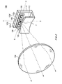
- Figs. 2 and 3 illustrate an exemplary structure of the light source unit 100.
- Fig. 2 is a perspective view of the light source unit 100
- Fig. 3 is a cross-sectional view thereof cut along a vertical plane parallel to the front-rear direction of the automobile.
- the light source unit 100 of this example is a projector-type light source unit for emitting light generated by a light source 120 ahead by means of a lens 104, and includes a supporting member 110, a light blocking member 112, the light source 120 and the lens 104.
- the supporting member 110 is a plate-like member that supports the bottom surface of the light source 120 on its surface facing ahead of the automobile so as to fix the light source 120, so that the light source 120 is allowed to emit light ahead of the automobile. Moreover, in this example, the supporting member 110 is arranged to standvertically. Thus, the supporting member 110 has a function of a heat sink that radiates heat generated by the light source 120. In this manner, it is possible to prevent reduction of light intensity of the light source 120 caused by the generated heat.
- the light blocking member 112 is a plate-like member provided to be opposed to the surface of the supporting member 110 with a part of the light source 120 sandwiched therebetween, and blocks a part of light generated by the light source 120 by covering the part of the light source 120 from the automobile-front side of the light source 120, that is a closer side to the front of the automobile.
- the light blocking member 112 blocks a part of the light generated by the light source 120 at its upper edge, thereby defining a boundary between a bright region and a dark region of light incident on the lens 104 based on the shape of the upper edge projected straight ahead of the upper edge.
- That projected shape of the upper edge is in form of a straight line extending in the approximately left-right direction of the automobile.
- That proj ected shape may be a shape with both ends turned down.
- the shape of the light blocking member 112 seen from above is such a shape that the light blocking member 112 crosses the light source unit 100 along the approximately transverse direction of the automobile while being curved backward at its center.
- the lower end of the light blocking member 112 is connected to the lower end of the supporting member 110, as shown in Fig. 2, and they are formed integrally with each other. Therefore, the light blocking member 112 receives heat generated by the light source 120 from the supporting member 110 . In this manner, the light blockingmember 112 has a function of a heat sink for radiating that heat.
- the light source 120 includes a plurality of semiconductor light emitting devices 102a-102e approximately aligned in a predetermined aligning direction.
- the light source 120 includes an odd number of semiconductor light emitting devices 102a-102e aligned in the approximately transverse direction of the automobile.
- Each of the semiconductor light emitting devices 102a-102e may be arranged in such a manner that the side at the lower end thereof extending in the approximately transverse direction is approximately aligned with the upper edge of the upper edge of the light blocking member 112.
- the lens 104 is an exemplary optical component provided commonly to a plurality of semiconductor light emitting devices 102a-102e.
- the lens 104 is arranged on the automotive-front side of the semiconductor light emitting devices 102a-102e, and transmits light emitted by those semiconductor light emitting devices 102a-102e, thereby irradiating that light toward the emitting direction ahead of the automobile.
- the lens 104 has an optical center F, that is a focus, a reference point in optical design or the like, on one of the odd number of semiconductor light emitting devices 102a-102e which is positioned at the center of them, i . e . , the semiconductor light emitting device 102c.
- the lens 104 has its optical center F on the intersection of X-axis and Y-axis.
- the X-axis and the Y-axis pass through the center of the surface of the semiconductor light emitting device 102c and the X-axis extends along the transverse direction of the automobile while the Y-axis extending vertically. In this case, it is possible to appropriately form the light distribution pattern having a symmetrical region.
- the semiconductor light emitting device 102c is arranged near the optical center F of the lens 104, the light source unit 100 can emit light that is controlled with high precision ahead.
- the lens 104 may have its optical center F in a predetermined area on the semiconductor light emitting device 102c that is set to correspond to the precision required for formation of the cut line.
- the lens 104 may have its optical center F on a position at the upper edge of the light blocking member 112 that is positioned in front of the semiconductor light emitting device 102c.
- the lens 104 may have its optical center F on the side at the lower end of the semiconductor light emitting device 102c extending in the lateral direction thereof.
- the lens 104 can clearly form the boundary between the bright region and the dark region corresponding to that side of the semiconductor light emitting device 102c ahead of the automobile by projecting an image of a region near that side of the semiconductor light emitting device 102c.
- the lens 104 may form at least a part of the cut line in the light distribution pattern of the automotive lamp 400 (see Fig. 1) based on light generated by the region near that side of the semiconductor light emitting device 102c, for example.
- the lens 104 may direct the light generated by the semiconductor light emitting device 102c to a region to be irradiated with light having especially higher illuminance, i.e., a so-called hot zone, near the cut line.
- the automotive lamp 400 can form the clear and appropriate cut line.
- the lens 104 may have its optical center F on any of other semiconductor light emitting devices 102a, 102b, 102d and 102e.
- the automotive lamp 400 can form the clear cut line by irradiating the region near the cut line with light appropriately.
- Fig. 4 illustrates an exemplary detailed structure of the light source 120.
- the light source 120 of this example is a linear light source extending in the approximately transverse direction of the automobile, and includes a substrate 106, a plurality of semiconductor light emitting devices 102a-102e and a light transmitting member 108.
- the substrate 106 fixes a plurality of semiconductor light emitting devices 102a-102e placed on its upper surface.
- the semiconductor light emitting devices 102a-102e are light emitting diodes, for example, and are approximately aligned at approximately constant intervals on the substrate 106.
- the semiconductor light emitting device 102 irradiates phosphors (not shown) provided on its surface with ultraviolet light so as to cause the phosphors to emit white light, for example.
- the semiconductor light emitting device may irradiate the phosphors with blue light so as to cause the phosphors to emit yellow light that is light of a complementary color of blue.
- the light source 120 emits white light based on the blue light and the yellow light respectively emitted by the semiconductor light emitting device and the phosphors.
- each of a plurality of semiconductor light emitting devices 102a-102e has a positive electrode 122 and a negative electrode 124 on its surface.
- the positive electrode 122 and the negative electrode 124 are provided to correspond to a P-type semiconductor layer and an N-type semiconductor layer (both not shown) in the semiconductor light emitting device 102, respectively, and receive power for generating light.
- the positive electrode 122 and the negative electrode 124 may be provided near a side substantially perpendicular to the aligning direction in which a plurality of semiconductor light emitting devices 102a-102e are arranged. In this case, the effect of the shape of the positive electrode 122 or negative electrode 124 on the formation of the cut line can be reduced.
- a plurality of semiconductor light emitting devices 102a-102e may be electrically connected in series by wirings (not shown) provided in the light source 120. In this case, the current flowing through the semiconductor light emitting devices 102a-102e can be made uniform. Alternatively, the semiconductor light emitting devices 102a-102e may be electrically connected in parallel. In this case, the voltage to be supplied to the light source can be reduced.
- the light transmitting member 108 is formed from material that can transmit light emitted by the semiconductor light emitting device 102, such as transparent resin, and seals a plurality of semiconductor light emitting devices 102a-102e by being formed to be opposed to the substrate 106 with those semiconductor light emitting devices 102a-102e sandwiched therebetween. According to this example, it is possible to appropriately form the light source 120 using a plurality of semiconductor light emitting devices 102a-102e.
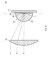
- Fig. 5 is a conceptual diagram of an exemplary light distribution pattern 302 formed by the light source unit 100.
- the light distribution pattern 302 is a light distribution pattern of a low beam formed on a virtual vertical screen arranged at a position 25 meters ahead of the light source unit 100.
- the lens 104 forms the light distribution pattern 302 having a predetermined shape by projecting light emitted by a plurality of semiconductor light emitting devices 102a-102e (see Fig. 2) onto the virtual vertical screen.
- the lens 104 forms a cut line in the light distribution pattern 302 based on the shape of the upper edge of the light blocking member 112 (see Fig. 2).
- the lens 104 irradiates light emitted by the semiconductor light emitting device 102c to a region 304 that is a part of the light distribution pattern 302.
- the lens 104 may form a boundary 306 of the region 304 on the cut line of the light distribution pattern 302 in accordance with the side at the lower end of the semiconductor light emitting device 102c.
- the lens 104 has its optical center F on the semiconductor light emitting device 102c.
- the lens 104 clearly projects the boundary 306 to a region near the hot zone around the center of the light distribution pattern 302.
- the lens 104 may form a portion in the cut line in the light distribution pattern 302, other than the boundary 306, in accordance with the sides at the lower ends of the semiconductor light emitting devices 102a, 102b, 102d and 102e, for example. In this case, it is possible to clearly form the cut line in the light distribution pattern 302 because those sides at the lower ends are positioned in a focal plane of the lens 104.
- the automotive lamp 400 may form the light distribution pattern 302 based on light generated by a plurality of light source units 100 respectively having different light distribution characteristics.
- each of those light source units 100 may irradiate a region that is a part of the light distribution pattern 302 with light.
- Fig. 6 shows another exemplary structure of the light source unit 100.
- the light source 120 includes an even number of semiconductor light emitting devices 102a-102f arranged in the approximately transverse direction of the automobile.
- the even number of semiconductor light emitting devices 102a-102f are arranged asymmetrically with respect to the optical center F of the lens 104.
- the lens 104 forms at least a part of the light distribution pattern of the automotive lamp 400 (see Fig. 1) based on light emitted by those semiconductor light emitting devices 102a-102f thus arranged.
- the lens 104 has its optical center F near the semiconductor light emitting device 102b.
- the lens 104 has its optical center F on the intersection of X-axis and Y-axis both running through the center of the surface of the semiconductor light emitting device 102b, X-axis extending in the transverse direction of the automobile while Y-axis extending vertically, as shown in Fig. 6.
- the lens 104 irradiates light ahead of the automobile on the left based on light generated by two semiconductor light emitting devices 102a and 102b and irradiates light of higher intensity ahead of the automobile on the right based on light emitted by the remaining four semiconductor light emitting devices 102c-102f, for example.
- the vehicular headlamp is required to have a light distribution pattern in which either of right and left sides of the automobile has to be irradiated with light of higher intensity, in accordance with a manner in which automobiles pass by each other that is determined by a law or the like. According to this example, it is possible to form an appropriate light distribution pattern.
- the light blocking member 112 is curved toward the rear of the automobile in such a manner that a portion of the light blocking member 112 near the semiconductor light emitting device 102b is the closest to the rear of the automobile.
- the automotive lamp 400 may further include a light source unit in addition to the aforementioned light source units 100, which has light distribution characteristics from those of the light source units 100.
- the automotive lamp 400 may form a desired light distribution pattern based on light emitted by a plurality of light source units respectively having different light distribution characteristics. According to this example, it is possible to appropriately form various light distribution patterns.
- the components in Fig. 6 having the same reference numerals as those in Fig. 2 have the same or similar functions as/to the components in Fig. 2 and therefore the description thereof is omitted.
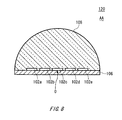
- Figs. 7 and 8 illustrate another exemplary structure of the light source 120 in detail.
- Fig. 7 shows the light source 120 seen from above, while Fig. 8 shows a cross section of the light source 120 taken along line A-A in Fig. 7.
- the substrate 106 is a disc.
- a plurality of semiconductor light emitting devices 102a-102e are approximately aligned in such a manner the sides of them are aligned on the virtual line A-A passing through the center of the circle formed by the outer periphery of the upper surface of the substrate 106, as shown in Fig. 7.
- the light transmittingmember 108 has an approximately hemispherical shape having its center at the center O of the aforementioned circle.
- One side of one of the semiconductor light emitting devices 102a-102e positioned at the center of them, i.e., the semiconductor light emitting device 102c is placed on the center O of the aforementioned circle.
- the semiconductor light emitting device 102c irradiates light generated by a portion near that side on the center O at such an angle with respect to the surface of the light transmitting member 108 that total reflection of that light does not occur. Therefore, the light transmitting member 108 can irradiate the light emitted by the semiconductor light emitting device 102 pass to the outside efficiently.
- the components in Figs. 7 and 8 having the same reference numerals as those in Fig. 4 have the same or similar functions as/to the components in Fig. 4 and therefore the description thereof is omitted.
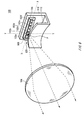
- Figs. 9 and 10 illustrate another exemplary structure of the light source unit 100.
- Fig. 9 is a perspective view of the light source unit 100
- Fig. 10 is a cross-sectional view thereof taken along a vertical cross section parallel to the front-rear direction of the automobile.
- the light source unit 100 makes light emitted by a plurality of semiconductor light emitting devices 102a-102e incident directly on the lens 104 without using the light blocking member 112 (see Fig. 2).
- the light source 120 has the same or similar function as/to that shown in Figs. 7 and 8.
- a plurality of semiconductor light emitting devices 102a-102e are fixed on the substrate 106 in such a manner their sides aligned on the virtual line A-A (see Fig. 7) are positioned at the lower ends, as shown in Fig. 9.
- the light source 120 may have the same or similar function and structure as/to the light source 120 shown in Fig. 4.
- the lens 104 has its optical center F on the side at the lower end of the semiconductor light emitting device 102c, as shown in Figs. 9 and 10.
- the lens 104 has its optical center F on the intersection of X-axis and Y-axis both running through the center of that side at the lower end of the semiconductor light emitting device 102c, X-axis extending in the transverse direction of the automobile while Y-axis extending vertically.
- the lens 104 forms at least a part of the cut line in the light distribution pattern by projecting an image of a portion near that side of the semiconductor light emitting device 102c.
- the light source unit 100 of this example forms a light distribution pattern that is similar to at least a part of the light distribution pattern 302 shown in Fig. 5.
- the lens 104 irradiates light emitted by the semiconductor light emitting device 102c to a region 304 that is a part of the light distribution pattern 302.
- the lens 104 forms a boundary 306 of the region 304 on the cut line in the light distribution pattern 302 in accordance with the side at the lower end of the semiconductor light emitting device 102c.
- the lens 104 may form the boundary 306 by projecting the light emitted by the semiconductor light emitting device 102c from an end face that contains that side.
- the automotive lamp 400 may form the light distribution pattern 302 based on light generated by a plurality of light source units 100 respectively having different light distribution characteristics. Except for the above, the components in Figs. 9 and 10 having the same reference numerals as those in Figs. 2 and 3 have the same or similar functions as the components in Figs. 2 and 3 and therefore the description thereof is omitted.
- Figs. 11 and 12 illustrate another exemplary structure of the light source unit 100.
- Figs. 11 and 12 are cross-sectional views of the light source unit 100 taken along a B-B vertical plane and an A-A horizontal plane, respectively.
- the light source unit 100 of this example is a projector-type light source unit that emits light reflected and converged at a position near the optical axis, ahead via a lens.
- the light source unit 100 includes a supportingmember 116, a light source 120, a reflecting mirror 118, a lens 104 and another reflecting mirror 114.
- the supporting member 116 is a plate having an upper surface arranged approximately horizontally, and fixes the bottom surface of the light source 120 placed on the upper surface thereof.
- the light source 120 includes a plurality of semiconductor light emitting devices 102a-102e and is fixed on the upper surface of the supporting member 116 to face up.
- the light source 120 may have the same or similar function as the light source 120 shown in Fig. 4.
- the semiconductor light emitting devices 102a-102e have sides extending in the approximately transverse direction of the automobile at their front and rear ends.
- the light source 120 may have the same or similar function as the light source 120 shown in Figs. 7 and 8.
- the reflecting mirror 118 reflects light at its upper surface that is arranged substantially horizontally, and is provided between the front end of the supporting member 116 and the lens 104.
- the reflecting mirror 118 may be provided in a plane substantially containing a plurality of semiconductor light emitting devices 102a-102e. In this case, light generated by the light source 120 can be made incident on the lens 104 efficiently.
- the front edge of the reflecting mirror 118 has an approximately linear shape that extends in the approximately transverse direction of the automobile. This front edge of the reflecting mirror 118 may have a shape in accordance with the cut line to be formed, such as a shape with both ends turned down.
- the lens 104 is provided on the automobile-front side of the reflecting mirrors 118 and 114 and transmits light reflected by the reflecting mirror 118 or 114 to direct that light toward the emitting direction ahead of the automobile.
- the lens 104 has a focus near the front edge of the reflecting mirror 118 and forms at least a part of the light distribution pattern of the automotive lamp 400 (see Fig. 1) by projecting an image of a focal plane containing the focus of the lens 104 ahead of the automobile.
- the lens 104 forms at least a part of the cut line in the light distribution pattern of the automotive lamp 400 based on the shape of the front edge of the reflecting mirror 118.
- the reflecting mirror 114 is an exemplary optical component provided commonly to a plurality of semiconductor light emitting diodes 102a-102e and is arranged to surround the light source 120 from behind, above and sides of the light source 120. In this manner, the reflecting mirror 114 reflects light generated by the light source 120 ahead, thereby making that light incident on the lens 104 and then making the lens 104 irradiate that light toward the emitting direction. Thus, the reflecting mirror 114 can irradiate light emitted by a plurality of semiconductor light emitting devices 102a-102e toward the emitting direction.
- At least a part of the reflecting mirror 114 has an approximately spheroidal shape formed by a combined elliptical plane, for example.
- This approximately spheroidal shape is set in such a manner that a cross section thereof containing the optical axis of the light source unit 100 forms at least a part of an approximately elliptical shape.
- the eccentricity of that approximately elliptical shape is set to gradually increase from that in the vertical cross section to that in the horizontal cross section.
- the light source unit 100 has the optical axis that runs approximately through the center of the lens 104 to go ahead of the automobile.
- the approximately spheroidal part of the reflecting mirror 114 has a focus F1, that is an exemplary optical center, near the one of the semiconductor light emitting devices 102a-102e positioned at the center of them, i.e., the semiconductor light emitting device 102c and also has a focus F2 near the front end of the reflecting mirror 118.
- that approximately spheroidal part has its optical center F on the intersection of X-axis and Y-axis both passing through the center of the surface of the semiconductor light emitting device 102c, X-axis extending in the transverse direction of the automobile while Y-axis extending vertically.
- that approximately spheroidal part converges at least most of the light generated by the light source 120 at a position near the front edge of the reflecting mirror 118.
- a clear boundary between a bright region and a dark region base on the shape of the front edge of the reflectingmirror 118 is formed near that front edge. Therefore, the lens 104 having its focus near that front edge can irradiate light having the clear boundary between the bright and dark regions to a region near the cut line in the light distribution pattern. Thus, according to this example, it is possible to appropriately form the light distribution pattern having the clear cut line.
- the approximately spheroidal part of the reflecting mirror 114 may have the focus F1 near the side at the front end of the semiconductor light emitting device 102c.
- that approximately spheroidal part makes at least most of the light emitted by the semiconductor light emitting devices 102a-102e incident directly on the lens 104 without making it incident on the reflecting mirror 118 . Therefore, it is possible to irradiate the region near the cut line with light more appropriately.
- the reflecting mirror 114 may be a parabolic reflecting mirror having its focus near the semiconductor light emitting device 102c.
- the light source unit 100 may be a parabolic light source unit that emits light ahead by using a parabolic reflecting mirror.
- Such a light source unit 100 has a transparent cover in place of the lens 104. In this case, the light source unit 100 can emit light controlled with high precision ahead.
Landscapes
- Engineering & Computer Science (AREA)
- Physics & Mathematics (AREA)
- Microelectronics & Electronic Packaging (AREA)
- Health & Medical Sciences (AREA)
- Life Sciences & Earth Sciences (AREA)
- General Engineering & Computer Science (AREA)
- Optics & Photonics (AREA)
- Power Engineering (AREA)
- Heart & Thoracic Surgery (AREA)
- Medical Informatics (AREA)
- Surgery (AREA)
- Animal Behavior & Ethology (AREA)
- General Health & Medical Sciences (AREA)
- Public Health (AREA)
- Veterinary Medicine (AREA)
- Biophysics (AREA)
- Pathology (AREA)
- Biomedical Technology (AREA)
- Molecular Biology (AREA)
- Condensed Matter Physics & Semiconductors (AREA)
- General Physics & Mathematics (AREA)
- Computer Hardware Design (AREA)
- Mechanical Engineering (AREA)
- Signal Processing (AREA)
- Computer Networks & Wireless Communication (AREA)
- Oral & Maxillofacial Surgery (AREA)
- Dentistry (AREA)
- Non-Portable Lighting Devices Or Systems Thereof (AREA)
- Led Device Packages (AREA)
Abstract
Description
- The present invention relates to a vehicular headlamp. More particularly, the present invention relates to a vehicular headlamp for emitting light toward a predetermined emitting direction. The vehicular headlamp the invention concerns, for example, regular headlamp, fog lamp and cornering lamp for automobiles, trains, motorcycles or the like.
- A vehicular headlamp for emitting light ahead of an automobile, for example, has to distribute the emitted light in a desired distribution pattern with high precision from safety reasons. That light distribution pattern is formed by means of an optical system using a reflecting mirror, a lens or the like, for example, as disclosed in Japanese Patent Application Publication (Laid-Open) No. 6-89601, pages 3-7 and Figs. 1-14. In recent years, the use of a semiconductor light emitting device in the vehicular headlamp has been discussed.
- In order to obtain sufficient light amount in the vehicular headlamp, a method has been discussed in which a plurality of semiconductor light emitting devices are used. In this case, however, optical design may become more complicated, resulting in difficulty in formation of an appropriate light distribution pattern.
- Therefore, it is an object of the present invention to provide a vehicular headlamp, which is capable of overcoming the above drawbacks accompanying the conventional art. The above and other obj ects can be achieved by combinations described in the independent claims. The dependent claims define further advantageous and exemplary combinations of the present invention.
- According to the first aspect of the present invention, a vehicular headlamp for emitting light toward a predetermined emitting direction, comprises: a plurality of semiconductor light emitting devices approximately aligned; and an optical component, having its optical center on one of the plurality of semiconductor light emitting devices, operable to irradiate light emitted by the plurality of semiconductor light emitting devices toward the emitting direction.
- The plurality of semiconductor light emitting device may be aligned in a predetermined aligning direction; the one semiconductor light emitting device may have a side at an end thereof, the side extending in the aligning direction; and the optical component may have the optical center on the side and may form at least a part of a cut line for defining a boundary between a bright region and a dark region in a light distribution pattern of the vehicular headlamp based on light emitted by a portion near the side of the one semiconductor light emitting device.
- The vehicular headlamp may emit the light ahead of an automobile, and the plurality of semiconductor light emitting devices may be aligned in an approximately transverse direction of the automobile.
- An odd number of semiconductor light emitting devices may be provided, and the optical component may have the optical center on one of the semiconductor light emitting devices that is positioned at a center of them.
- An even number of semiconductor light emitting devices may be provided, the semiconductor light emitting devices being arranged asymmetrically with respect to the optical center of the optical component, and the optical component may form at least a part of a light distribution pattern of the vehicular headlamp based on the light emitted by the semiconductor light emitting devices.
- The vehicular headlamp to which the present invention may be applied to includes but not limited to regular headlamp, fog lamp and cornering lamp for automobiles, trains, motorcycles or the like.
- The summary of the invention does not necessarily describe all necessary features of the present invention. The present invention may also be a sub-combination of the features described above. The above and other features and advantages of the present invention will become more apparent from the following description of the embodiments taken in conjunction with the accompanying drawings.
- Fig. 1 illustrates an exemplary structure of an automotive lamp according to the present invention.
- Fig. 2 is a perspective view of an exemplary light source unit.
- Fig. 3 is a cross-sectional view of the light source unit shown in Fig. 2.
- Fig. 4 shows an exemplary structure of a light source in detail.
- Fig. 5 is a conceptual diagram of an exemplary light distribution pattern.
- Fig. 6 shows the structure of another exemplary light source unit.
- Fig. 7 is a top view of another exemplary light source.
- Fig. 8 is a cross-sectional view of the light source shown in Fig. 7, taken along A-A line in Fig. 7.
- Fig. 9 is a perspective view of another exemplary light source unit.
- Fig. 10 is a cross-sectional view of the light source unit shown in Fig. 9.
- Fig. 11 is a cross-sectional view of another exemplary light source unit, taken along a vertical plane thereof.
- Fig. 12 is a cross-sectional view of the light source unit, taken along a horizontal plane thereof.
- The invention will now be described based on the preferred embodiments, which do not intend to limit the scope of the present invention, but exemplify the invention. All of the features and the combinations thereof described in the embodiment are not necessarily essential to the invention.
- Fig. 1 illustrates an exemplary structure of an
automotive lamp 400 according to an embodiment of the present invention. Theautomotive lamp 400 is a vehicular headlamp for emitting a low beam that emits light toward a predetermined emitting direction ahead of an automobile. Theautomotive lamp 400 of this example aims to clearly form a cut line that defines a boundary between a bright region and a dark region in a light distribution pattern of the vehicular headlamp. Theautomotive lamp 400 accommodates a plurality oflight source units 100 approximately aligned in a row within a lamp room formed by atransparent cover 402 and alamp body 404. - Those
light source units 100 have the same or similar structure. Thelight source units 100 are accommodated in the lamp room in such a manner those optical axes are at a downward angle of about 0.3° to about 0.6° with respect to the front-rear direction of the automobile when theautomotive lamp 400 is mounted on the body of the automobile. Theautomotive lamp 400 forms a predetermined light distribution pattern by emitting light ahead of the automobile based on the light emitted by thoselight source units 100. Theautomotive lamp 400 may include a plurality oflight source units 100 respectively having different light distribution characteristics. - Figs. 2 and 3 illustrate an exemplary structure of the
light source unit 100. Fig. 2 is a perspective view of thelight source unit 100, while Fig. 3 is a cross-sectional view thereof cut along a vertical plane parallel to the front-rear direction of the automobile. Thelight source unit 100 of this example is a projector-type light source unit for emitting light generated by alight source 120 ahead by means of alens 104, and includes a supportingmember 110, alight blocking member 112, thelight source 120 and thelens 104. - The supporting
member 110 is a plate-like member that supports the bottom surface of thelight source 120 on its surface facing ahead of the automobile so as to fix thelight source 120, so that thelight source 120 is allowed to emit light ahead of the automobile. Moreover, in this example, the supportingmember 110 is arranged to standvertically. Thus, the supportingmember 110 has a function of a heat sink that radiates heat generated by thelight source 120. In this manner, it is possible to prevent reduction of light intensity of thelight source 120 caused by the generated heat. - The
light blocking member 112 is a plate-like member provided to be opposed to the surface of the supportingmember 110 with a part of thelight source 120 sandwiched therebetween, and blocks a part of light generated by thelight source 120 by covering the part of thelight source 120 from the automobile-front side of thelight source 120, that is a closer side to the front of the automobile. - In this example, the
light blocking member 112 blocks a part of the light generated by thelight source 120 at its upper edge, thereby defining a boundary between a bright region and a dark region of light incident on thelens 104 based on the shape of the upper edge projected straight ahead of the upper edge. That projected shape of the upper edge is in form of a straight line extending in the approximately left-right direction of the automobile. That proj ected shape may be a shape with both ends turned down. In this example, the shape of thelight blocking member 112 seen from above is such a shape that thelight blocking member 112 crosses thelight source unit 100 along the approximately transverse direction of the automobile while being curved backward at its center. - In this example, the lower end of the
light blocking member 112 is connected to the lower end of the supportingmember 110, as shown in Fig. 2, and they are formed integrally with each other. Therefore, thelight blocking member 112 receives heat generated by thelight source 120 from the supportingmember 110 . In this manner, thelight blockingmember 112 has a function of a heat sink for radiating that heat. - The
light source 120 includes a plurality of semiconductorlight emitting devices 102a-102e approximately aligned in a predetermined aligning direction. In this example, thelight source 120 includes an odd number of semiconductorlight emitting devices 102a-102e aligned in the approximately transverse direction of the automobile. Each of the semiconductorlight emitting devices 102a-102e may be arranged in such a manner that the side at the lower end thereof extending in the approximately transverse direction is approximately aligned with the upper edge of the upper edge of thelight blocking member 112. - The
lens 104 is an exemplary optical component provided commonly to a plurality of semiconductorlight emitting devices 102a-102e. Thelens 104 is arranged on the automotive-front side of the semiconductorlight emitting devices 102a-102e, and transmits light emitted by those semiconductorlight emitting devices 102a-102e, thereby irradiating that light toward the emitting direction ahead of the automobile. - The
lens 104 has an optical center F, that is a focus, a reference point in optical design or the like, on one of the odd number of semiconductorlight emitting devices 102a-102e which is positioned at the center of them, i . e . , the semiconductorlight emitting device 102c. In this example, thelens 104 has its optical center F on the intersection of X-axis and Y-axis. The X-axis and the Y-axis pass through the center of the surface of the semiconductorlight emitting device 102c and the X-axis extends along the transverse direction of the automobile while the Y-axis extending vertically. In this case, it is possible to appropriately form the light distribution pattern having a symmetrical region. Moreover, since the semiconductorlight emitting device 102c is arranged near the optical center F of thelens 104, thelight source unit 100 can emit light that is controlled with high precision ahead. - The
lens 104 may have its optical center F in a predetermined area on the semiconductorlight emitting device 102c that is set to correspond to the precision required for formation of the cut line. For example, thelens 104 may have its optical center F on a position at the upper edge of thelight blocking member 112 that is positioned in front of the semiconductorlight emitting device 102c. - Moreover, the
lens 104 may have its optical center F on the side at the lower end of the semiconductorlight emitting device 102c extending in the lateral direction thereof. In this case, thelens 104 can clearly form the boundary between the bright region and the dark region corresponding to that side of the semiconductorlight emitting device 102c ahead of the automobile by projecting an image of a region near that side of the semiconductorlight emitting device 102c. - The
lens 104 may form at least a part of the cut line in the light distribution pattern of the automotive lamp 400 (see Fig. 1) based on light generated by the region near that side of the semiconductorlight emitting device 102c, for example. Thelens 104 may direct the light generated by the semiconductorlight emitting device 102c to a region to be irradiated with light having especially higher illuminance, i.e., a so-called hot zone, near the cut line. In this case, theautomotive lamp 400 can form the clear and appropriate cut line. - In an alternative example, the
lens 104 may have its optical center F on any of other semiconductorlight emitting devices automotive lamp 400 can form the clear cut line by irradiating the region near the cut line with light appropriately. - Fig. 4 illustrates an exemplary detailed structure of the
light source 120. Thelight source 120 of this example is a linear light source extending in the approximately transverse direction of the automobile, and includes asubstrate 106, a plurality of semiconductorlight emitting devices 102a-102e and alight transmitting member 108. Thesubstrate 106 fixes a plurality of semiconductorlight emitting devices 102a-102e placed on its upper surface. - The semiconductor
light emitting devices 102a-102e are light emitting diodes, for example, and are approximately aligned at approximately constant intervals on thesubstrate 106. The semiconductor light emitting device 102 irradiates phosphors (not shown) provided on its surface with ultraviolet light so as to cause the phosphors to emit white light, for example. Alternatively, the semiconductor light emitting device may irradiate the phosphors with blue light so as to cause the phosphors to emit yellow light that is light of a complementary color of blue. In this case, thelight source 120 emits white light based on the blue light and the yellow light respectively emitted by the semiconductor light emitting device and the phosphors. - In this example, each of a plurality of semiconductor
light emitting devices 102a-102e has apositive electrode 122 and anegative electrode 124 on its surface. Thepositive electrode 122 and thenegative electrode 124 are provided to correspond to a P-type semiconductor layer and an N-type semiconductor layer (both not shown) in the semiconductor light emitting device 102, respectively, and receive power for generating light. Thepositive electrode 122 and thenegative electrode 124 may be provided near a side substantially perpendicular to the aligning direction in which a plurality of semiconductorlight emitting devices 102a-102e are arranged. In this case, the effect of the shape of thepositive electrode 122 ornegative electrode 124 on the formation of the cut line can be reduced. - Moreover, a plurality of semiconductor
light emitting devices 102a-102e may be electrically connected in series by wirings (not shown) provided in thelight source 120. In this case, the current flowing through the semiconductorlight emitting devices 102a-102e can be made uniform. Alternatively, the semiconductorlight emitting devices 102a-102e may be electrically connected in parallel. In this case, the voltage to be supplied to the light source can be reduced. - The
light transmitting member 108 is formed from material that can transmit light emitted by the semiconductor light emitting device 102, such as transparent resin, and seals a plurality of semiconductorlight emitting devices 102a-102e by being formed to be opposed to thesubstrate 106 with those semiconductorlight emitting devices 102a-102e sandwiched therebetween. According to this example, it is possible to appropriately form thelight source 120 using a plurality of semiconductorlight emitting devices 102a-102e. - Fig. 5 is a conceptual diagram of an exemplary
light distribution pattern 302 formed by thelight source unit 100. Thelight distribution pattern 302 is a light distribution pattern of a low beam formed on a virtual vertical screen arranged at a position 25 meters ahead of thelight source unit 100. - According to this example, the
lens 104 forms thelight distribution pattern 302 having a predetermined shape by projecting light emitted by a plurality of semiconductorlight emitting devices 102a-102e (see Fig. 2) onto the virtual vertical screen. Thelens 104 forms a cut line in thelight distribution pattern 302 based on the shape of the upper edge of the light blocking member 112 (see Fig. 2). For example, thelens 104 irradiates light emitted by the semiconductorlight emitting device 102c to aregion 304 that is a part of thelight distribution pattern 302. In this case, thelens 104 may form aboundary 306 of theregion 304 on the cut line of thelight distribution pattern 302 in accordance with the side at the lower end of the semiconductorlight emitting device 102c. - As described referring to Fig. 2, the
lens 104 has its optical center F on the semiconductorlight emitting device 102c. In this case, thelens 104 clearly projects theboundary 306 to a region near the hot zone around the center of thelight distribution pattern 302. Thus, it is possible to clearly form the cut line of thelight distribution pattern 302. - The
lens 104 may form a portion in the cut line in thelight distribution pattern 302, other than theboundary 306, in accordance with the sides at the lower ends of the semiconductorlight emitting devices light distribution pattern 302 because those sides at the lower ends are positioned in a focal plane of thelens 104. - In an alternative example, the automotive lamp 400 (see Fig. 1) may form the
light distribution pattern 302 based on light generated by a plurality oflight source units 100 respectively having different light distribution characteristics. In this case, each of thoselight source units 100 may irradiate a region that is a part of thelight distribution pattern 302 with light. - Fig. 6 shows another exemplary structure of the
light source unit 100. In this example, thelight source 120 includes an even number of semiconductorlight emitting devices 102a-102f arranged in the approximately transverse direction of the automobile. The even number of semiconductorlight emitting devices 102a-102f are arranged asymmetrically with respect to the optical center F of thelens 104. In this case, thelens 104 forms at least a part of the light distribution pattern of the automotive lamp 400 (see Fig. 1) based on light emitted by those semiconductorlight emitting devices 102a-102f thus arranged. - The
lens 104 has its optical center F near the semiconductorlight emitting device 102b. In this example, thelens 104 has its optical center F on the intersection of X-axis and Y-axis both running through the center of the surface of the semiconductorlight emitting device 102b, X-axis extending in the transverse direction of the automobile while Y-axis extending vertically, as shown in Fig. 6. Thelens 104 irradiates light ahead of the automobile on the left based on light generated by two semiconductorlight emitting devices light emitting devices 102c-102f, for example. - It should be noted that in some cases the vehicular headlamp is required to have a light distribution pattern in which either of right and left sides of the automobile has to be irradiated with light of higher intensity, in accordance with a manner in which automobiles pass by each other that is determined by a law or the like. According to this example, it is possible to form an appropriate light distribution pattern. Please note that the
light blocking member 112 is curved toward the rear of the automobile in such a manner that a portion of thelight blocking member 112 near the semiconductorlight emitting device 102b is the closest to the rear of the automobile. - In this example, the
automotive lamp 400 may further include a light source unit in addition to the aforementionedlight source units 100, which has light distribution characteristics from those of thelight source units 100. In this case, theautomotive lamp 400 may form a desired light distribution pattern based on light emitted by a plurality of light source units respectively having different light distribution characteristics. According to this example, it is possible to appropriately form various light distribution patterns. Except for the above, the components in Fig. 6 having the same reference numerals as those in Fig. 2 have the same or similar functions as/to the components in Fig. 2 and therefore the description thereof is omitted. - Figs. 7 and 8 illustrate another exemplary structure of the
light source 120 in detail. Fig. 7 shows thelight source 120 seen from above, while Fig. 8 shows a cross section of thelight source 120 taken along line A-A in Fig. 7. - In this example, the
substrate 106 is a disc. A plurality of semiconductorlight emitting devices 102a-102e are approximately aligned in such a manner the sides of them are aligned on the virtual line A-A passing through the center of the circle formed by the outer periphery of the upper surface of thesubstrate 106, as shown in Fig. 7. - The
light transmittingmember 108 has an approximately hemispherical shape having its center at the center O of the aforementioned circle. One side of one of the semiconductorlight emitting devices 102a-102e positioned at the center of them, i.e., the semiconductorlight emitting device 102c is placed on the center O of the aforementioned circle. In this case, the semiconductorlight emitting device 102c irradiates light generated by a portion near that side on the center O at such an angle with respect to the surface of thelight transmitting member 108 that total reflection of that light does not occur. Therefore, thelight transmitting member 108 can irradiate the light emitted by the semiconductor light emitting device 102 pass to the outside efficiently. Except for the above, the components in Figs. 7 and 8 having the same reference numerals as those in Fig. 4 have the same or similar functions as/to the components in Fig. 4 and therefore the description thereof is omitted. - Figs. 9 and 10 illustrate another exemplary structure of the
light source unit 100. Fig. 9 is a perspective view of thelight source unit 100, while Fig. 10 is a cross-sectional view thereof taken along a vertical cross section parallel to the front-rear direction of the automobile. In this example, thelight source unit 100 makes light emitted by a plurality of semiconductorlight emitting devices 102a-102e incident directly on thelens 104 without using the light blocking member 112 (see Fig. 2). - The
light source 120 has the same or similar function as/to that shown in Figs. 7 and 8. A plurality of semiconductorlight emitting devices 102a-102e are fixed on thesubstrate 106 in such a manner their sides aligned on the virtual line A-A (see Fig. 7) are positioned at the lower ends, as shown in Fig. 9. Thelight source 120 may have the same or similar function and structure as/to thelight source 120 shown in Fig. 4. - The
lens 104 has its optical center F on the side at the lower end of the semiconductorlight emitting device 102c, as shown in Figs. 9 and 10. In this example, thelens 104 has its optical center F on the intersection of X-axis and Y-axis both running through the center of that side at the lower end of the semiconductorlight emitting device 102c, X-axis extending in the transverse direction of the automobile while Y-axis extending vertically. In this case, thelens 104 forms at least a part of the cut line in the light distribution pattern by projecting an image of a portion near that side of the semiconductorlight emitting device 102c. - The
light source unit 100 of this example forms a light distribution pattern that is similar to at least a part of thelight distribution pattern 302 shown in Fig. 5. Thelens 104 irradiates light emitted by the semiconductorlight emitting device 102c to aregion 304 that is a part of thelight distribution pattern 302. In this case, thelens 104 forms aboundary 306 of theregion 304 on the cut line in thelight distribution pattern 302 in accordance with the side at the lower end of the semiconductorlight emitting device 102c. Thelens 104 may form theboundary 306 by projecting the light emitted by the semiconductorlight emitting device 102c from an end face that contains that side. - According to this example, it is possible to form an appropriate light distribution pattern. The automotive lamp 400 (see Fig. 1) may form the
light distribution pattern 302 based on light generated by a plurality oflight source units 100 respectively having different light distribution characteristics. Except for the above, the components in Figs. 9 and 10 having the same reference numerals as those in Figs. 2 and 3 have the same or similar functions as the components in Figs. 2 and 3 and therefore the description thereof is omitted. - Figs. 11 and 12 illustrate another exemplary structure of the
light source unit 100. Figs. 11 and 12 are cross-sectional views of thelight source unit 100 taken along a B-B vertical plane and an A-A horizontal plane, respectively. Thelight source unit 100 of this example is a projector-type light source unit that emits light reflected and converged at a position near the optical axis, ahead via a lens. Thelight source unit 100 includes asupportingmember 116, alight source 120, a reflectingmirror 118, alens 104 and another reflectingmirror 114. - The supporting
member 116 is a plate having an upper surface arranged approximately horizontally, and fixes the bottom surface of thelight source 120 placed on the upper surface thereof. Thelight source 120 includes a plurality of semiconductorlight emitting devices 102a-102e and is fixed on the upper surface of the supportingmember 116 to face up. Thelight source 120 may have the same or similar function as thelight source 120 shown in Fig. 4. The semiconductorlight emitting devices 102a-102e have sides extending in the approximately transverse direction of the automobile at their front and rear ends. Alternatively, thelight source 120 may have the same or similar function as thelight source 120 shown in Figs. 7 and 8. - The reflecting
mirror 118 reflects light at its upper surface that is arranged substantially horizontally, and is provided between the front end of the supportingmember 116 and thelens 104. The reflectingmirror 118 may be provided in a plane substantially containing a plurality of semiconductorlight emitting devices 102a-102e. In this case, light generated by thelight source 120 can be made incident on thelens 104 efficiently. Moreover, the front edge of the reflectingmirror 118 has an approximately linear shape that extends in the approximately transverse direction of the automobile. This front edge of the reflectingmirror 118 may have a shape in accordance with the cut line to be formed, such as a shape with both ends turned down. - The
lens 104 is provided on the automobile-front side of the reflectingmirrors mirror lens 104 has a focus near the front edge of the reflectingmirror 118 and forms at least a part of the light distribution pattern of the automotive lamp 400 (see Fig. 1) by projecting an image of a focal plane containing the focus of thelens 104 ahead of the automobile. In this case, thelens 104 forms at least a part of the cut line in the light distribution pattern of theautomotive lamp 400 based on the shape of the front edge of the reflectingmirror 118. - The reflecting
mirror 114 is an exemplary optical component provided commonly to a plurality of semiconductorlight emitting diodes 102a-102e and is arranged to surround thelight source 120 from behind, above and sides of thelight source 120. In this manner, the reflectingmirror 114 reflects light generated by thelight source 120 ahead, thereby making that light incident on thelens 104 and then making thelens 104 irradiate that light toward the emitting direction. Thus, the reflectingmirror 114 can irradiate light emitted by a plurality of semiconductorlight emitting devices 102a-102e toward the emitting direction. - In this example, at least a part of the reflecting
mirror 114 has an approximately spheroidal shape formed by a combined elliptical plane, for example. This approximately spheroidal shape is set in such a manner that a cross section thereof containing the optical axis of thelight source unit 100 forms at least a part of an approximately elliptical shape. The eccentricity of that approximately elliptical shape is set to gradually increase from that in the vertical cross section to that in the horizontal cross section. In addition, thelight source unit 100 has the optical axis that runs approximately through the center of thelens 104 to go ahead of the automobile. - The approximately spheroidal part of the reflecting
mirror 114 has a focus F1, that is an exemplary optical center, near the one of the semiconductorlight emitting devices 102a-102e positioned at the center of them, i.e., the semiconductorlight emitting device 102c and also has a focus F2 near the front end of the reflectingmirror 118. In this example, that approximately spheroidal part has its optical center F on the intersection of X-axis and Y-axis both passing through the center of the surface of the semiconductorlight emitting device 102c, X-axis extending in the transverse direction of the automobile while Y-axis extending vertically. In this case, that approximately spheroidal part converges at least most of the light generated by thelight source 120 at a position near the front edge of the reflectingmirror 118. - In this case, a clear boundary between a bright region and a dark region base on the shape of the front edge of the
reflectingmirror 118 is formed near that front edge. Therefore, thelens 104 having its focus near that front edge can irradiate light having the clear boundary between the bright and dark regions to a region near the cut line in the light distribution pattern. Thus, according to this example, it is possible to appropriately form the light distribution pattern having the clear cut line. - The approximately spheroidal part of the reflecting
mirror 114 may have the focus F1 near the side at the front end of the semiconductorlight emitting device 102c. In this case, that approximately spheroidal part makes at least most of the light emitted by the semiconductorlight emitting devices 102a-102e incident directly on thelens 104 without making it incident on the reflectingmirror 118 . Therefore, it is possible to irradiate the region near the cut line with light more appropriately. - In another example, the reflecting
mirror 114 may be a parabolic reflecting mirror having its focus near the semiconductorlight emitting device 102c. In this case, thelight source unit 100 may be a parabolic light source unit that emits light ahead by using a parabolic reflecting mirror. Such alight source unit 100 has a transparent cover in place of thelens 104. In this case, thelight source unit 100 can emit light controlled with high precision ahead. - As is apparent from the above description, according to the present invention, it is possible to appropriately form a light distribution pattern.
- Although the present invention has been described by way of exemplary embodiments, it should be understood that those skilled in the art might make many changes and substitutions without departing from the scope of the present invention which is defined by the appended claims.
Claims (5)
- A vehicular headlamp for emitting light toward a predetermined emitting direction, comprising:a plurality of semiconductor light emitting devices approximately aligned; andan optical component, having its optical center on one of said plurality of semiconductor light emitting devices, operable to irradiate light emitted by said plurality of semiconductor light emitting devices toward said emitting direction.
- A vehicular headlamp as claimed in claim 1, wherein said plurality of semiconductor light emitting device are aligned in a predetermined aligning direction;
said one semiconductor light emitting device has a side at an end thereof, said side extending in said aligning direction; and
said optical component has said optical center on said side and forms at least a part of a cut line for defining a boundary between a bright region and a dark region in a light distribution pattern of said vehicular headlamp based on light emitted by a portion near said side of said one semiconductor light emitting device. - A vehicular headlamp as claimed in claim 1 or 2, wherein said vehicular headlamp emits said light ahead of an automobile, and
said plurality of semiconductor light emitting devices are aligned in an approximately transverse direction of the automobile. - A vehicular headlanp as claimed in any of the preceding claims, wherein an odd number of semiconductor light emitting devices are provided, and
said optical component has said optical center on one of said semiconductor light emitting devices that is positioned at a center of them. - A vehicular headlanp as claimed in any of the preceding claims, wherein an even number of semiconductor light emitting devices are provided, said semiconductor light emitting devices being arranged asymmetrically with respect to said optical center of said optical component, and
said optical component forms at least a part of a light distribution pattern of said vehicular headlamp based on said light emitted by said semiconductor light emitting devices.
Applications Claiming Priority (2)
| Application Number | Priority Date | Filing Date | Title |
|---|---|---|---|
| JP2003035253 | 2003-02-13 | ||
| JP2003035253A JP4083593B2 (en) | 2003-02-13 | 2003-02-13 | Vehicle headlamp |
Publications (3)
| Publication Number | Publication Date |
|---|---|
| EP1447616A2 true EP1447616A2 (en) | 2004-08-18 |
| EP1447616A3 EP1447616A3 (en) | 2005-09-28 |
| EP1447616B1 EP1447616B1 (en) | 2009-07-15 |
Family
ID=32677608
Family Applications (1)
| Application Number | Title | Priority Date | Filing Date |
|---|---|---|---|
| EP04003010A Expired - Lifetime EP1447616B1 (en) | 2003-02-13 | 2004-02-11 | Vehicular headlamp |
Country Status (6)
| Country | Link |
|---|---|
| US (1) | US7128453B2 (en) |
| EP (1) | EP1447616B1 (en) |
| JP (1) | JP4083593B2 (en) |
| KR (1) | KR100544077B1 (en) |
| CN (1) | CN100578074C (en) |
| DE (1) | DE602004021982D1 (en) |
Cited By (14)
| Publication number | Priority date | Publication date | Assignee | Title |
|---|---|---|---|---|
| FR2853393A1 (en) * | 2003-02-06 | 2004-10-08 | Koito Mfg Co Ltd | VEHICLE HEADLIGHT WITH PHOTOEMISSIVE DIODE |
| FR2858045A1 (en) * | 2003-07-24 | 2005-01-28 | Koito Mfg Co Ltd | Lamp unit for vehicle headlight, has stopper unit whose upper edge is placed at proximity of optical axis such that lower part of light emitted by light emitting diode is stopped |
| EP1487025A3 (en) * | 2003-06-13 | 2006-03-01 | Stanley Electric Co., Ltd. | Light emitting diode for light source of a vehicle headlamp |
| WO2006034668A2 (en) * | 2004-09-30 | 2006-04-06 | Osram Opto Semiconductors Gmbh | Led array with temperature sensor |
| EP1645466A1 (en) * | 2004-10-07 | 2006-04-12 | Yamaha Hatsudoki Kabushiki Kaisha | Method for controlling lighting means of a vehicle and vehicle |
| EP1526581A3 (en) * | 2003-08-20 | 2006-05-17 | Stanley Electric Co., Ltd. | Light source and vehicle lamp |
| US7246930B2 (en) | 2003-09-17 | 2007-07-24 | Stanley Electric Co., Ltd. | Light source and vehicle lamp |
| CN100404357C (en) * | 2004-10-07 | 2008-07-23 | 雅马哈发动机株式会社 | Method for controlling lighting region of a two-wheeled motorcycle and two-wheeled motorcycle light |
| US7484872B2 (en) | 2003-10-24 | 2009-02-03 | Stanley Electric Co., Ltd. | Vehicle lamp |
| DE102008044676A1 (en) * | 2008-08-28 | 2010-03-04 | Delvis Gmbh | Lighting System for motorcycle, particularly road racing bicycle, has head lamp, particularly central head lamp which is arranged in longitudinal axis of motorcycle |
| WO2010032143A1 (en) | 2008-09-18 | 2010-03-25 | Philips Intellectual Property & Standards Gmbh | Lighting unit and vehicle headlamp |
| EP2338729A1 (en) * | 2009-12-22 | 2011-06-29 | Automotive Lighting Reutlingen GmbH | Light module for a motor vehicle headlamp |
| US8258527B2 (en) | 2008-06-09 | 2012-09-04 | Stanley Electric Co., Ltd. | Lighting device and semiconductor light source device |
| EP3021368A1 (en) * | 2014-11-11 | 2016-05-18 | LG Innotek Co., Ltd. | Light-emitting apparatus |
Families Citing this family (35)
| Publication number | Priority date | Publication date | Assignee | Title |
|---|---|---|---|---|
| JP4251941B2 (en) * | 2003-08-08 | 2009-04-08 | 三菱電機株式会社 | head lamp |
| JP2005332640A (en) * | 2004-05-18 | 2005-12-02 | Ichikoh Ind Ltd | Vehicular head light unit |
| US7419839B2 (en) | 2004-11-12 | 2008-09-02 | Philips Lumileds Lighting Company, Llc | Bonding an optical element to a light emitting device |
| WO2006082537A1 (en) * | 2005-02-02 | 2006-08-10 | Philips Intellectual Property & Standards Gmbh | Light-source module and holder therefor |
| US7744225B2 (en) * | 2005-03-15 | 2010-06-29 | Casio Computer Co., Ltd. | Light source apparatus that collects and provides different-colored light rays emitted by a plurality of different-colored light sources and a projector comprising such light source apparatus |
| JP4675874B2 (en) * | 2006-01-20 | 2011-04-27 | 株式会社小糸製作所 | Lighting fixtures for vehicles |
| JP4663548B2 (en) * | 2006-02-24 | 2011-04-06 | 株式会社小糸製作所 | Vehicle headlamp lamp unit |
| CN100441525C (en) * | 2006-04-20 | 2008-12-10 | 上海交通大学 | Method for preparing filtration material for earthworm biofilter |
| US7648257B2 (en) * | 2006-04-21 | 2010-01-19 | Cree, Inc. | Light emitting diode packages |
| US7264387B1 (en) | 2006-05-08 | 2007-09-04 | Visteon Global Technologies, Inc. | Reduced depth projector headlamp assembly |
| JP4729441B2 (en) * | 2006-06-09 | 2011-07-20 | スタンレー電気株式会社 | Vehicle lighting |
| US20080025037A1 (en) * | 2006-07-28 | 2008-01-31 | Visteon Global Technologies, Inc. | LED headlamp |
| JP2008243434A (en) * | 2007-03-26 | 2008-10-09 | Koito Mfg Co Ltd | Lamp tool unit of vehicle headlight |
| JP2008258001A (en) * | 2007-04-05 | 2008-10-23 | Koito Mfg Co Ltd | Lamp unit of vehicular headlamp |
| JP5033530B2 (en) * | 2007-07-27 | 2012-09-26 | スタンレー電気株式会社 | Light source unit for vehicle lamp |
| KR100963966B1 (en) * | 2007-11-21 | 2010-06-15 | 현대모비스 주식회사 | ??? unit and optical source module therewith |
| US7690826B2 (en) * | 2007-11-29 | 2010-04-06 | Sl Seobong | Adaptive front light system using LED headlamp |
| JP2009266434A (en) | 2008-04-22 | 2009-11-12 | Koito Mfg Co Ltd | Light source module and lighting fixture for vehicle |
| JP4618571B2 (en) * | 2008-12-19 | 2011-01-26 | スタンレー電気株式会社 | Light source device for vehicle headlamp |
| JPWO2010150459A1 (en) * | 2009-06-23 | 2012-12-06 | 株式会社小糸製作所 | Light emitting module |
| CN101698552B (en) * | 2009-11-09 | 2012-08-29 | 南京大学 | Method for treating domestic sewage with reinforced capillary infiltration trench system |
| US8931920B2 (en) * | 2010-01-14 | 2015-01-13 | Osram Sylvania Inc. | Optic for an LED array |
| CN102791522B (en) * | 2010-03-19 | 2015-07-15 | 皇家飞利浦电子股份有限公司 | Lighting assembly for vehicle |
| TW201300258A (en) * | 2011-06-30 | 2013-01-01 | Phoenix Optronics Corp | Method of using lens imaging to control headlight hotspot |
| EP2752615A4 (en) * | 2011-09-01 | 2015-07-08 | Koito Mfg Co Ltd | Automotive headlamp apparatus |
| DE102011112285A1 (en) * | 2011-09-05 | 2013-03-07 | Schott Ag | Optical device for use as e.g. illumination device and for illuminating e.g. road sign, has lenses arranged in small distance to surface of light sources, where one of lenses focuses light in direction and forms light on defined geometry |
| JP5879876B2 (en) * | 2011-09-28 | 2016-03-08 | スタンレー電気株式会社 | Vehicle lamp unit |
| CN102691959B (en) * | 2012-06-21 | 2016-05-25 | 刘德润 | Headlamp LED light source |
| CN103672664B (en) | 2012-09-26 | 2017-03-01 | 中强光电股份有限公司 | Lighting device for vehicle |
| KR20160056089A (en) * | 2014-11-11 | 2016-05-19 | 엘지이노텍 주식회사 | Light emitting apparatus |
| KR102294317B1 (en) * | 2015-01-30 | 2021-08-26 | 엘지이노텍 주식회사 | Light emitting apparatus |
| CN106524038B (en) * | 2016-11-30 | 2023-05-23 | 武汉通畅汽车电子照明有限公司 | Multi-light source module and automobile lamp |
| JP2017174830A (en) * | 2017-06-27 | 2017-09-28 | 株式会社小糸製作所 | Lamp tool unit |
| JP7221659B2 (en) * | 2017-11-17 | 2023-02-14 | スタンレー電気株式会社 | semiconductor light emitting device |
| RU2747225C1 (en) * | 2020-10-19 | 2021-04-29 | Общество с ограниченной ответственностью "Диодосвет" | Adaptive front lighting system |
Citations (3)
| Publication number | Priority date | Publication date | Assignee | Title |
|---|---|---|---|---|
| US20010019486A1 (en) | 2000-03-01 | 2001-09-06 | Vincent Thominet | Illumination device for vehicle |
| JP2003031011A (en) | 2001-07-16 | 2003-01-31 | Stanley Electric Co Ltd | Linear light source for lighting fixture |
| JP2003031007A (en) | 2001-07-16 | 2003-01-31 | Stanley Electric Co Ltd | Lighting tool |
Family Cites Families (11)
| Publication number | Priority date | Publication date | Assignee | Title |
|---|---|---|---|---|
| HU191444B (en) * | 1984-09-21 | 1987-02-27 | Tungsram Rt,Hu | Reflector lamp |
| US4883333A (en) * | 1987-10-13 | 1989-11-28 | Yanez Serge J | Integrated, solid, optical device |
| JPH071804B2 (en) * | 1989-02-15 | 1995-01-11 | シャープ株式会社 | Light emitting element array light source |
| JP2787745B2 (en) | 1992-09-04 | 1998-08-20 | 株式会社小糸製作所 | Vehicle headlight reflector |
| FR2700404B1 (en) * | 1993-01-11 | 1995-03-31 | Reflexion Plus | Barcode sticker reader, of the so-called "hand-held" type with increased depth of field. |
| JPH11232912A (en) | 1998-02-16 | 1999-08-27 | Pfu Ltd | Led illuminating structure |
| US6227669B1 (en) * | 1998-05-26 | 2001-05-08 | Industrial Technology Research Institute | Illumination device and image projection apparatus comprising the device |
| JP2001177156A (en) | 1999-12-14 | 2001-06-29 | Koha Co Ltd | Side emitting led lamp |
| DE10129743C2 (en) * | 2001-06-20 | 2003-05-08 | Daimler Chrysler Ag | Vehicle headlight, with a number of electronic lighting elements as the light source |
| JP4089866B2 (en) * | 2001-10-12 | 2008-05-28 | スタンレー電気株式会社 | Light projecting unit and LED vehicle illumination lamp comprising the light projecting unit |
| JP4158140B2 (en) * | 2002-05-14 | 2008-10-01 | スタンレー電気株式会社 | Vehicle lighting |
-
2003
- 2003-02-13 JP JP2003035253A patent/JP4083593B2/en not_active Expired - Fee Related
-
2004
- 2004-02-10 KR KR1020040008662A patent/KR100544077B1/en not_active IP Right Cessation
- 2004-02-11 DE DE602004021982T patent/DE602004021982D1/en not_active Expired - Lifetime
- 2004-02-11 US US10/776,996 patent/US7128453B2/en not_active Expired - Lifetime
- 2004-02-11 EP EP04003010A patent/EP1447616B1/en not_active Expired - Lifetime
- 2004-02-11 CN CN200410005351A patent/CN100578074C/en not_active Expired - Fee Related
Patent Citations (3)
| Publication number | Priority date | Publication date | Assignee | Title |
|---|---|---|---|---|
| US20010019486A1 (en) | 2000-03-01 | 2001-09-06 | Vincent Thominet | Illumination device for vehicle |
| JP2003031011A (en) | 2001-07-16 | 2003-01-31 | Stanley Electric Co Ltd | Linear light source for lighting fixture |
| JP2003031007A (en) | 2001-07-16 | 2003-01-31 | Stanley Electric Co Ltd | Lighting tool |
Cited By (25)
| Publication number | Priority date | Publication date | Assignee | Title |
|---|---|---|---|---|
| US7631997B2 (en) | 2003-02-06 | 2009-12-15 | Koito Manufacturing Co., Ltd. | Vehicular headlamp and light emission module |
| FR2853393A1 (en) * | 2003-02-06 | 2004-10-08 | Koito Mfg Co Ltd | VEHICLE HEADLIGHT WITH PHOTOEMISSIVE DIODE |
| US7312477B2 (en) | 2003-06-13 | 2007-12-25 | Stanley Electric Co., Ltd. | Led lamp for light source |
| EP1487025A3 (en) * | 2003-06-13 | 2006-03-01 | Stanley Electric Co., Ltd. | Light emitting diode for light source of a vehicle headlamp |
| US8093613B2 (en) | 2003-06-13 | 2012-01-10 | Stanley Electric Co., Ltd. | LED lamp for light source |
| US7622748B2 (en) | 2003-06-13 | 2009-11-24 | Stanley Electric Co., Ltd. | LED lamp for light source and method |
| FR2858045A1 (en) * | 2003-07-24 | 2005-01-28 | Koito Mfg Co Ltd | Lamp unit for vehicle headlight, has stopper unit whose upper edge is placed at proximity of optical axis such that lower part of light emitted by light emitting diode is stopped |
| US8506147B2 (en) | 2003-08-20 | 2013-08-13 | Stanley Electric Co., Ltd. | Light source and vehicle lamp |
| EP1526581A3 (en) * | 2003-08-20 | 2006-05-17 | Stanley Electric Co., Ltd. | Light source and vehicle lamp |
| US7645062B2 (en) | 2003-08-20 | 2010-01-12 | Stanley Electric Co., Ltd. | Light source and vehicle lamp |
| US7246930B2 (en) | 2003-09-17 | 2007-07-24 | Stanley Electric Co., Ltd. | Light source and vehicle lamp |
| US7753573B2 (en) | 2003-09-17 | 2010-07-13 | Stanley Electric Co., Ltd. | Light source and vehicle lamp |
| US7950837B2 (en) | 2003-10-24 | 2011-05-31 | Stanley Electric Co., Ltd. | Vehicle lamp |
| US7484872B2 (en) | 2003-10-24 | 2009-02-03 | Stanley Electric Co., Ltd. | Vehicle lamp |
| WO2006034668A3 (en) * | 2004-09-30 | 2006-11-02 | Osram Opto Semiconductors Gmbh | Led array with temperature sensor |
| WO2006034668A2 (en) * | 2004-09-30 | 2006-04-06 | Osram Opto Semiconductors Gmbh | Led array with temperature sensor |
| CN100404357C (en) * | 2004-10-07 | 2008-07-23 | 雅马哈发动机株式会社 | Method for controlling lighting region of a two-wheeled motorcycle and two-wheeled motorcycle light |
| EP1645466A1 (en) * | 2004-10-07 | 2006-04-12 | Yamaha Hatsudoki Kabushiki Kaisha | Method for controlling lighting means of a vehicle and vehicle |
| US8258527B2 (en) | 2008-06-09 | 2012-09-04 | Stanley Electric Co., Ltd. | Lighting device and semiconductor light source device |
| DE102008044676A1 (en) * | 2008-08-28 | 2010-03-04 | Delvis Gmbh | Lighting System for motorcycle, particularly road racing bicycle, has head lamp, particularly central head lamp which is arranged in longitudinal axis of motorcycle |
| WO2010032143A1 (en) | 2008-09-18 | 2010-03-25 | Philips Intellectual Property & Standards Gmbh | Lighting unit and vehicle headlamp |
| US9631785B2 (en) | 2008-09-18 | 2017-04-25 | Koninklijke Philips N.V. | Lighting unit and vehicle headlamp |
| EP2338729A1 (en) * | 2009-12-22 | 2011-06-29 | Automotive Lighting Reutlingen GmbH | Light module for a motor vehicle headlamp |
| EP3021368A1 (en) * | 2014-11-11 | 2016-05-18 | LG Innotek Co., Ltd. | Light-emitting apparatus |
| US10191185B2 (en) | 2014-11-11 | 2019-01-29 | Lg Innotek Co., Ltd. | Light-emitting apparatus |
Also Published As
| Publication number | Publication date |
|---|---|
| CN1521444A (en) | 2004-08-18 |
| JP4083593B2 (en) | 2008-04-30 |
| JP2004247150A (en) | 2004-09-02 |
| DE602004021982D1 (en) | 2009-08-27 |
| EP1447616A3 (en) | 2005-09-28 |
| US20040160783A1 (en) | 2004-08-19 |
| US7128453B2 (en) | 2006-10-31 |
| CN100578074C (en) | 2010-01-06 |
| KR100544077B1 (en) | 2006-01-23 |
| KR20040073330A (en) | 2004-08-19 |
| EP1447616B1 (en) | 2009-07-15 |
Similar Documents
| Publication | Publication Date | Title |
|---|---|---|
| EP1447616B1 (en) | Vehicular headlamp | |
| EP1447617B1 (en) | Vehicular headlamp | |
| JP4024721B2 (en) | Vehicle lamp and light source module | |
| KR100570481B1 (en) | Vehicle headlamp | |
| KR100570480B1 (en) | Vehicle headlamp | |
| JP5157883B2 (en) | Vehicle headlamp | |
| US7108412B2 (en) | Headlamp for vehicle | |
| US6948836B2 (en) | Light source unit having orthogonally disposed semiconductor light emitter | |
| US7972046B2 (en) | Vehicle lighting device | |
| WO2009131125A1 (en) | Light source module and lighting device for vehicle | |
| US20050162857A1 (en) | Lamp unit for vehicle and illumination lamp for vehicle | |
| US7118260B2 (en) | Lamp unit for vehicle | |
| US20050105301A1 (en) | Lamp | |
| US20090080210A1 (en) | Motor Vehicle Headlight | |
| KR20040020838A (en) | Vehicle headlamp | |
| CN114688494B (en) | Lamp for vehicle | |
| JP2012156051A (en) | Vehicle headlamp | |
| JP6161504B2 (en) | Automotive headlamp | |
| KR101232047B1 (en) | Headlight for vehicles | |
| WO2023189597A1 (en) | Vehicle lamp |
Legal Events
| Date | Code | Title | Description |
|---|---|---|---|
| PUAI | Public reference made under article 153(3) epc to a published international application that has entered the european phase |
Free format text: ORIGINAL CODE: 0009012 |
|
| AK | Designated contracting states |
Kind code of ref document: A2 Designated state(s): AT BE BG CH CY CZ DE DK EE ES FI FR GB GR HU IE IT LI LU MC NL PT RO SE SI SK TR |
|
| AX | Request for extension of the european patent |
Extension state: AL LT LV MK |
|
| PUAL | Search report despatched |
Free format text: ORIGINAL CODE: 0009013 |
|
| AK | Designated contracting states |
Kind code of ref document: A3 Designated state(s): AT BE BG CH CY CZ DE DK EE ES FI FR GB GR HU IE IT LI LU MC NL PT RO SE SI SK TR |
|
| AX | Request for extension of the european patent |
Extension state: AL LT LV MK |
|
| RIC1 | Information provided on ipc code assigned before grant |
Ipc: 7F 21S 8/10 B Ipc: 7F 21W 101:10 Z Ipc: 7F 21Y 101:02 Z Ipc: 7F 21S 8/12 A Ipc: 7H 01L 25/075 B Ipc: 7B 60Q 1/00 B |
|
| 17P | Request for examination filed |
Effective date: 20060303 |
|
| AKX | Designation fees paid |
Designated state(s): DE FR GB |
|
| 17Q | First examination report despatched |
Effective date: 20080925 |
|
| GRAP | Despatch of communication of intention to grant a patent |
Free format text: ORIGINAL CODE: EPIDOSNIGR1 |
|
| RIC1 | Information provided on ipc code assigned before grant |
Ipc: H01L 25/075 20060101ALI20090205BHEP Ipc: F21W 101/10 20060101ALI20090205BHEP Ipc: F21Y 101/02 20060101ALI20090205BHEP Ipc: F21S 8/10 20060101ALI20090205BHEP Ipc: F21S 8/12 20060101AFI20090205BHEP Ipc: B60Q 1/00 20060101ALI20090205BHEP |
|
| GRAS | Grant fee paid |
Free format text: ORIGINAL CODE: EPIDOSNIGR3 |
|
| GRAA | (expected) grant |
Free format text: ORIGINAL CODE: 0009210 |
|
| AK | Designated contracting states |
Kind code of ref document: B1 Designated state(s): DE FR GB |
|
| REG | Reference to a national code |
Ref country code: GB Ref legal event code: FG4D |
|
| REF | Corresponds to: |
Ref document number: 602004021982 Country of ref document: DE Date of ref document: 20090827 Kind code of ref document: P |
|
| PLBE | No opposition filed within time limit |
Free format text: ORIGINAL CODE: 0009261 |
|
| STAA | Information on the status of an ep patent application or granted ep patent |
Free format text: STATUS: NO OPPOSITION FILED WITHIN TIME LIMIT |
|
| 26N | No opposition filed |
Effective date: 20100416 |
|
| PGFP | Annual fee paid to national office [announced via postgrant information from national office to epo] |
Ref country code: GB Payment date: 20140206 Year of fee payment: 11 |
|
| GBPC | Gb: european patent ceased through non-payment of renewal fee |
Effective date: 20150211 |
|
| REG | Reference to a national code |
Ref country code: FR Ref legal event code: PLFP Year of fee payment: 13 |
|
| PG25 | Lapsed in a contracting state [announced via postgrant information from national office to epo] |
Ref country code: GB Free format text: LAPSE BECAUSE OF NON-PAYMENT OF DUE FEES Effective date: 20150211 |
|
| REG | Reference to a national code |
Ref country code: FR Ref legal event code: PLFP Year of fee payment: 14 |
|
| REG | Reference to a national code |
Ref country code: DE Ref legal event code: R079 Ref document number: 602004021982 Country of ref document: DE Free format text: PREVIOUS MAIN CLASS: F21S0008120000 Ipc: F21S0041000000 |
|
| REG | Reference to a national code |
Ref country code: FR Ref legal event code: PLFP Year of fee payment: 15 |
|
| PGFP | Annual fee paid to national office [announced via postgrant information from national office to epo] |
Ref country code: FR Payment date: 20190111 Year of fee payment: 16 Ref country code: DE Payment date: 20190129 Year of fee payment: 16 |
|
| REG | Reference to a national code |
Ref country code: DE Ref legal event code: R119 Ref document number: 602004021982 Country of ref document: DE |
|
| PG25 | Lapsed in a contracting state [announced via postgrant information from national office to epo] |
Ref country code: FR Free format text: LAPSE BECAUSE OF NON-PAYMENT OF DUE FEES Effective date: 20200229 Ref country code: DE Free format text: LAPSE BECAUSE OF NON-PAYMENT OF DUE FEES Effective date: 20200901 |