EP1445681A2 - Method and apparatus for clock synthesis using universal serial bus downstream received signals - Google Patents
Method and apparatus for clock synthesis using universal serial bus downstream received signals Download PDFInfo
- Publication number
- EP1445681A2 EP1445681A2 EP04250430A EP04250430A EP1445681A2 EP 1445681 A2 EP1445681 A2 EP 1445681A2 EP 04250430 A EP04250430 A EP 04250430A EP 04250430 A EP04250430 A EP 04250430A EP 1445681 A2 EP1445681 A2 EP 1445681A2
- Authority
- EP
- European Patent Office
- Prior art keywords
- bit
- signal
- oscillator
- bits
- responsive
- Prior art date
- Legal status (The legal status is an assumption and is not a legal conclusion. Google has not performed a legal analysis and makes no representation as to the accuracy of the status listed.)
- Granted
Links
Images








Classifications
-
- G—PHYSICS
- G06—COMPUTING OR CALCULATING; COUNTING
- G06F—ELECTRIC DIGITAL DATA PROCESSING
- G06F1/00—Details not covered by groups G06F3/00 - G06F13/00 and G06F21/00
- G06F1/04—Generating or distributing clock signals or signals derived directly therefrom
Definitions
- the present invention concerns an internal reference clock for Universal Serial Bus (“USB”) devices, and more particularly, concerns generating the reference clock making use of an integrated, free running oscillator metered by downstream received USB signals D+ and D- sent by a USB host or hub.
- USB Universal Serial Bus
- USB devices need an accurate clock for reasons described hereafter.
- a host or hub sends downstream data to a USB device there is a need at the device end to sample this data stream to recognize the logical states of the data, i.e. "1's" and "0's".
- the sampling clock must have a frequency similar to the one timing the downstream traffic in the host or hub.
- the sampling clock must have a frequency similar to the one timing the upstream traffic in the device.
- the host or hub and the device clock frequencies are similar since both the device and the host or hub have clocks based on quartz crystal or piezo resonator.
- a Full Speed (“FS”) device clock needs to sample received data or drive transmittal data at an average rate of 12Mbit per second ⁇ 0.25 % while synchronized to the host or hub clock, and vice versa.
- Quartz crystal or piezo resonator based clock generators have conventionally been used to provide both the high level of accuracy of the average rate and the small jitters.
- a USB device receives and sends data on a "USB" bus, i.e., a bus that meets requirements of the USB2.0 Specification with or without the On-The-Go supplement (“OTG”), comprising V BUS , GND, D+ and D-.
- a USB device has typically at least one printed circuit board (“PCB”) with at least one integrated circuit (“IC”) with pins connected to one or more other components onto the PCB.
- PCB printed circuit board
- IC integrated circuit
- USB devices configured in this manner include for example, mass storage devices, some employing flash memory technology and others employing compact disk technology, printer devices or camera devices.
- At least one pin of an IC is used to connect the quartz crystal or piezo resonator located on the PCB externally to the IC.
- the extra pins dedicated to connecting the quartz crystal or piezo resonator to the IC are a relatively small proportion of the IC's overall pins, and the quartz crystal or the piezo resonator occupies a relatively small portion of the overall PCB area. Consequently, in those devices, a quartz crystal or piezo resonator is compatible with their overall architecture.
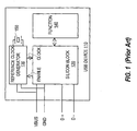
- a USB device 110 includes at least one silicon block 120 with integrated circuitry for a serial engine, transceivers and data stream manager to receive downstream signals and send upstream signals on a USB's D+ and D- lines and to manage data links to and from a function 140.
- the USB device 110 brings to the user function 140 such as mass storage devices, printer device or camera device mentioned before.
- the device 110 is powered by V BUS when bus-powered, or by an external power supply when self-powered.
- FIG. 1 represents a bus-powered device 110 in a generalized fashion without depicting any specific function 140.
- function 140 may be merged into a single silicon block.
- the reference clock generator 130 delivers a clock to the silicon block 120.
- the reference clock generator 130 contains at least one IC associated with the quartz crystal or the piezo resonator to generate an electrical signal serving the silicon block 120 clock needs.
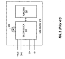
- FIG. 2 represents aspects of another prior art arrangement for a device 210 where a quartz crystal or piezo resonator 250 is connected to a silicon block 220.
- the silicon block 220 of FIG. 2 receives downstream signals and transmits upstream signals on a USB's D+ and D- lines as well as manages data streams from and to a function 240.
- the clock generator is included with the serial engine, transceivers, and data streams manager integrated circuitry on a single silicon block 220.
- the function 240 may likewise be merged onto silicon block 220.
- USB devices 110 and 120 of FIG.'s 1 and 2 are problematic for certain applications. These applications include a new family of USB devices, removable secure content (“RSC”) devices, connected directly to a Personal Computer (“PC”) USB port, or any enabled USB host such as OTG dual role device or Set Top Boxes through a simple pass through connector with possibly decoupling capacitors and inrush current limiting series resistor.
- RSC removable secure content
- PC Personal Computer
- RSC devices enable a new range of applications such as user authentication, platform Log On, Public Key Infrastructure, and also Digital Right Management for Voice Over the Internet Protocol (VOIP), cable TV, Digital Subscriber Line (DSL), where there is a need for data streaming while deciphering, or data storage for medical and other personal information such as banking account.
- VOIP Voice Over the Internet Protocol
- DSL Digital Subscriber Line
- Those devices have the Token form factor or preferably the Smart Card form factor, form factors, which are well known.
- USB-ICC USB Integrated Chip Card
- ISO 7816-2 the USB Integrated Chip Card
- USB-ICC's have only eight external contacts to which pins of a single IC are interconnected.
- C1, C4, C5 and C8 are used to connect respectively V BUS , D+, GND and D-.
- a quartz crystal or a piezo resonator cannot be connected to the IC of a USB-ICC within a required card thickness of less than 850 ⁇ m.
- USB-ICC and other USB RSC devices have to be power consumption conscious, since they can be connected to battery powered USB hosts such as laptop computers, mobile phones and Personal Digital Assistants.
- the latter two devices may be dual-role OTG devices with limited current availability for bus-powered devices. For example, in these applications power consumption is limited to less than few hundreds of microamperes for operation while in suspend state.
- a RSC device will be preferably implemented making use of a single chip to be embedded into a Smart Card or a Subscriber Identification Module (SIM), which will enable massive diffusion. All plastic credit card and Digital Right Management (DRM) cards could be equipped with such a chip in a near future.
- SIM Subscriber Identification Module
- DRM Digital Right Management
- One application in the WiFi or 802.11 context, could be for the removable secure content device to secure transactions as well as serving as a SIM.
- the power consumption performance is of prime importance.
- Leydier, et al. disclose the use of USB downstream signals on D+ and D- to generate a clock on a single IC used for receiving and transmitting data without a quartz crystal or a piezo resonator and Leydier, et al. further disclose a method and a device for recovering the clock from the signals D+ and D- sent by a host or a hub in the context of a USB Low-Speed ("LS") device.
- the disclosed method and device are implemented in an IC to generate a clock in a USB-ICC or a RSC device working in LS.
- the method disclosed by Bruhnke removes extra pulses from a local clock in order to produce a stabilized stream of pulses. Specifically, at Bruhnke, page 6, starting at line 15, it is described that each thirty-fourth pulse is removed from the clock 12. The resulting number of pulses matches the theoretical number of pulses per millisecond ("ms"), in terms of an average data rate per ms, but for almost all the pulses in the stabilized pulse stream the pace from pulse-to-pulse is faster than the required average data rate by more than the permissible error of ⁇ 0.25%. Therefore, the technique disclosed by Bruhnke, to selectively remove extra clock pulses, is problematic regarding jitter performances.
- the present invention concerns an internal reference clock for Universal Serial Bus (“USB”) devices, and more particularly, concerns generating the reference clock making use of an integrated, free running oscillator metered by downstream received USB signals D+ and D- sent by a USB host or hub.
- the free running oscillator which does not make use of a quartz crystal or a piezo resonator as in prior art, is stable and initially inaccurate.
- the free running oscillator initial inaccuracy, thermal drift and aging are compensated for by ongoing calibrations from downstream received USB signals D+ and D-, which results in generating a reference clock with performance compatible with both source average bit rate accuracy and source jitters specified for Full Speed (“FS”) devices.
- the reference clock samples the downstream traffic and pulses the upstream traffic.
- FIG. 1 illustrates a first prior art USB device.
- FIG. 2 illustrates a second prior art USB device.
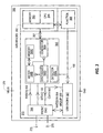
- FIG. 3 illustrates a high level view of a USB device, according to an embodiment of the present invention.
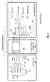
- FIG. 4 illustrates the USB device of FIG. 3 in more detail in a downstream traffic situation, according to an embodiment of the present invention.
- FIG. 5 illustrates the USB device of FIG. 3 in more detail in an upstream traffic situation according to an embodiment of the present invention.
- FIG. 6 illustrates a flow diagram, according to an embodiment of the present invention.
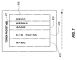
- FIG. 7 illustrates a symbolic representation of a SETUP token packet as per USB2.0.
- FIG. 8 illustrates a time diagram of the SETUP token packet of FIG. 7 FIG.
- FIG. 9 illustrates a symbolic representation of consecutive Start Of Frame (“SOF") tokens as per USB 2.0.
- FIG. 10 illustrates aspects of a High-Speed Oscillator ("HSO"), according to an embodiment of the present invention.
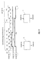
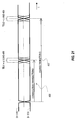
- FIG. 11 illustrates a time diagram of a portion of one of the SOF tokens of FIG. 9 and illustrates aspects of generating secondary signals RXDD4 and RXDD8 from a received RXDDW of the token, according to an embodiment of the present invention.
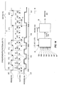
- FIG. 12 illustrates aspects of metering duration of the RXDD4 signal of FIG. 11 using the outputs of the HSO of FIG. 9 to generate a number M of one-eighth periods of HSO, according to an embodiment of the present invention.
- FIG. 13 illustrates aspects of metering duration of the RXDD8 signal of FIG. 11 using the outputs of the HSO of FIG. 9 to generate a number N of one-eighth periods of HSO, according to an embodiment of the present invention.
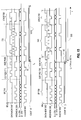
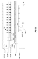
- FIG. 14 illustrates a time diagram of a portion of one of the SOF tokens of FIG. 9 and illustrates aspects of decoding the downstream signal RXDDW to generate NRZIDDW.
- FIG. 15 illustrates, in a time diagram, certain details of two consecutives SOF tokens and related signal Consecutive Start Of Frame (“CSOF”), in terms of significance with respect to an embodiment of the present invention.
- CSOF Consecutive Start Of Frame
- FIG. 16 illustrates a sub logic block generating a secondary signal CSOF from the received RXDDW signal, according to an embodiment of the present invention.
- FIG. 17 illustrates aspects of metering the CSOF signal duration using an output of the HSO of FIG. 9.
- FIG. 18 illustrates logic for clock circuitry, according to an embodiment of the present invention.
- FIG. 19 illustrates a more detailed flow diagram according to an embodiment of the present invention.
- FIG. 20 illustrates aspects of generating upstream FS traffic on D+ and D-, according to an embodiment of the present invention.
- FIG. 21 illustrates certain aspects of the USB specification jitter requirements, in terms of significance with respect to an embodiment of the present invention.
- FIG. 22 illustrates the first milliseconds after a USB FS device receives power, according to an embodiment of the present invention.
- FIG. 3 represents a silicon block 370 integrating its clock without making use of any quartz crystal or resonator in a preferred embodiment of the present invention.
- a high level view of a USB device 390 is shown, according to an embodiment of the present invention.
- the clock 395 of the USB device 390 is fully integrated on a silicon block 370 without making use of a quartz crystal or a piezo resonator.
- a function 398 of the USB device 390 may be integrated on the same silicon block 370. This will be preferably the case if the function 398 provides memory 393 or performs cryptography or other calculation done by a Central Processing Unit (“CPU”) 394. If this is the case, all is fully integrated on the silicon block 370 including connections to V BUS , GND, D+ 376 and D- 375, and including circuitry for a front end 396, USB engine 397, and clock 395.
- CPU Central Processing Unit
- the CPU 394 and memory 393 interface with the clock 395 via interfaces 392.
- the clock 395 includes a generator 395A, a meter 395B, a memory 395C, a synthesizer 395D, and a detector 395E.
- the function 398 brought to the user is also connected to the USB serial engine 397.
- Detector 395E tracks a bit pattern received by the serial engine 397 via NRZIDDW 804.
- the USB device 390 of FIG. 3 is depicted in more detail in a downstream traffic situation, along with a host or hub 300.
- the host or hub 300 driven by a quartz crystal or a piezo resonator 350 sends downstream traffic to a USB device 390.
- the hub or host 300 includes a driver 315 that drives the D+ 376 line responsive to an input TXDPH and an input TXENH.
- the host or hub 300 also includes a driver 320 that drives the D- 375 line responsive to an input TXDMH and an input TXENH.
- TXENH enables both transmitters 315 and 320.
- the D+ 376 and D- 375 lines of the cable 365 terminate at respective load resistors 330 and 325.
- the data on DATAHDW 305 are pulsed on the bus by a clock making use of a quartz crystal or a piezo resonator 350.
- the USB device 390 has the silicon block 370 removably coupled to pass through connectors 360 and cable 365. For clarity, a decoupling capacitor between V BUS and GND, close to the bus powered device 390, as well as the inrush current limiting resistor in series with V BUS , are not shown. As previously stated, the silicon block 370, the only active component of the depicted USB device 390, does not make use of a quartz crystal or a piezo resonator.
- the clock CLK1X 803 is built in the silicon block 370 according to an embodiment of the present invention as depicted on FIG.3. Clock 395, Front-end 396 (including differential amplifier 377, switches 372, 373 and 374, pull up resistor 371 and VTERM) USB engine 397, and associated functions are all included on the silicon block 370.
- one end of an integrated pull up resistor 371 on silicon block 370 is connected to an integrated voltage reference VTERM, the other end is connected to D+ 376, D- 375 or left open, as follows.
- Switch 374 is on when the device 390 is not attached to the USB, in which case the host or the hub 300 cannot detect it.
- Switch 373 is on, thereby conductively coupling the reference voltage VTERM to D+ 376 when the device 390 is attached to the USB and performs as a FS device.
- Switch 372 is on, thereby conductively coupling the reference voltage VTERM to D- 375 when the device 390 is attached to the USB and performs as a LS device. According to the embodiment depicted only one of the switches, 374, 373 or 372 is on at given time.
- a differential receiver 377 receives signals from the host or hub 300 on the D+ 376 and D- 375 lines and responsively generates a single ended signal RXDDW 802. When D+ 376 is greater than D- 375, receiver 377 drives RXDDW 802 high. When D+ 376 is less than D- 375, receiver 377 drives RXDDW 802 low.
- clock 395 (FIG. 3) synthesizes a local clock signal CLKIX 803 for receiving downstream traffic.
- a speed signal 100 is generated by front end 396 responsive to switches 373 and 372.
- USB device 390 is again shown, this time in the context of upstream traffic to the host or hub 300.
- the front-end 396 of USB device 390 includes integrated drivers 382 and 383.
- Driver 382 drives the D+ 376 line responsive to an input TXDPD and an input TXEND.
- Driver 383 drives the D- 375 line responsive to an input TXDMD and an input TXEND.
- TXEND enables both transmitters 382 and 383.
- NRZIUP 385 data are pulsed on D+ 376 and the inverted NRZIUP 385 on D- 375 by CLK1X 803 from clock 395 (FIG. 3).
- a differential receiver 340 receives signals from the device 390 on the D+ 376 and D- 375 lines and responsively generates a single ended signal RXDHUP 355.
- RXDHUP 355. When D+ is greater than D-, receiver 340 drives RXDHUP 355 high.
- receiver 377 drives RXDHUP 355 low.
- the NRZIUP 345 data stream is detected by circuitry 310 sampling RXDHUP 355 with a clock making use of a quartz crystal or a piezo resonator 350.
- Known bit patterns sent downstream to device 390 by the host or hub 300 clocked by the quartz crystal or piezo resonator 350 driven circuitry were received (FIG. 4), as will be described further herein below.
- the clock 395 (FIG. 3), synthesizes a local clock signal CLKIX 803 for pulsing upstream traffic.
- a D+ and D- received downstream USB token Start Of Frame starts with a synchronization pattern ("SP").
- Clock 395 (FIG. 3 and also described further herein below) detects a known pattern of bits in SP and in other parts of the SOF. Responsive to detecting the known pattern, clock 395 (FIG.3) meters the generator 395A and adjusts its selection of the generator 395A output signals in order to generate a more accurate but still relatively coarse USB device clock signal CLKIX 803.
- the coarse clock defined at step 260 is used to scan unknown patterns and detect consecutive SOF's time marks delimiting a theoretical number of bits S equal to 12,000 sent by host or hub 300 (FIG. 4) at a theoretical average speed of 12Mbits per second. SOFs are broadcasted to FS devices every millisecond ⁇ 0.05%.
- clock 395 uses results from step 265, that is, meters with the generator 395A period the duration of S equal to 12,000 theoretical bits, which occur in one millisecond ⁇ 0.05%. With the metering results, the clock 395 adjusts again its selection of the generator 395A output signals, in order to generate a precise local clock signal CLKIX 803, i.e. accuracy better than ⁇ 0.25%.
- This precise clock signal CLKIX 803 pulses upstream traffic with accurate average data rate and controlled jitter.
- this clock CLK1X 803 will help receiving downstream as well.
- the loop back 275 indicates the ongoing aspect of the process, according to which recurrent adjustments of CLKIX 803 are made responsive to consecutive received SOF, thus compensating for initial inaccuracy, thermal drift and aging of the generator 395A period.
- a SETUP token 400 is illustrated, as sent by a host or hub 300 (FIG. 4) to USB device 390 in a LS or FS mode.
- SETUP token 400 is significant, and is therefore depicted here because it can be the first packet received by a LS device facing a host or a hub.
- Such tokens 400 include four bytes as shown, namely a SP (or merely "Sync") byte 410, a Packet Identifier PID byte 415, seven bits address ADDR 416 for the address of the target USB device 390 to which the SETUP token 400 is sent, a six bit endpoint number ENDP0 417 for the endpoint number of this target USB device 390. Finally, a five bits Cyclic Redundancy Check (“CRC”) CRC5 418. ADDR, ENDP0, and CRC bits are fully contained in two bytes.
- CRC Cyclic Redundancy Check
- An LS device when the USB is idle, is characterized by the fact that D- 375 is at a voltage greater than the voltage on D+. On such an LS device, switch 372 is on. On an LS device, switch 372 (FIG. 4) is on. The host or hub 300 (FIG. 4) recognizes LS devices and broadcasts LS packets only to LS devices. In the LS mode, the average data throughput is 1.5Mbit per second ⁇ 1.5% for upstream traffic. As mentioned above, LS devices do not receive SOF.
- DATAHDW 305 is the downstream data traffic sent by the host or hub 300.
- NRZIHDW 306 is the data traffic DATAHDW 305 coded in a non-return-to-zero protocol driving bus lines D+ 376 and D- 375 through drivers 315 and 320 (FIG. 4).
- the front-end 396 (FIG. 4) of the receiving device 390 (FIG. 4) generates RXDDW 802. Since, as previously stated, the SETUP token 400 can be the first received packet by such an LS device 390, and that generator 395A signals in clock 395 (FIG. 3) can be metered with this known received data pattern sent with ⁇ 0.25% accuracy, for example eight bit period 303, to synthesize a local clock signal CLKIX 803 (FIG. 4) for LS device 390 to be precise at ⁇ 1.5%.
- USB FS communication in addition to broadcasting data, host or hub 300 (FIG. 4) periodically broadcast the previously mentioned, SOF tokens 700, of which two are shown. These SOF tokens 700 are responded to by receiving USB devices 390 operating in FS mode, switch 373 is on (FIG. 4), but not by devices 390 operating in LS mode, switch 372 is on (FIG. 4).
- the tokens 700 include four bytes as shown.
- the first two bytes are a SYNC byte 710 and a PID byte 715.
- the Frame Number (“FRAME") 720 and the CRC5 725 are fully contained in two more bytes. Each will be described further in connection with FIG. 11, FIG. 14 and FIG.15.
- the SOF tokens 700 indicate frame interval timing, which, as previously stated, are broadcasted every millisecond ⁇ 0.05% by the host and repeated by any hub.
- the frame interval of one millisecond ⁇ 0.05% is measured from any point in a SOF token in one frame to the same point in the SOF token of the successive frame.
- the hubs' accuracy of the average data bit rate must be better than ⁇ 0.25% but they are required to keep the timing between two consecutive SOF as close as possible to one millisecond.
- Frame timing adjustment in hubs compensate for their own frequency inaccuracy, for example, a hub having a -0.2% clock will time a theoretical 11,976 of its own clock between two successive SOFs it repeats from the host.
- Leydier, et al. disclose a device and a method making use of known received downstream signals D+ and D- metering a stable and initially inaccurate, free running oscillator period, the result being used to synthesize a local clock. Further details, for a device and method, have been disclosed therein specifically for LS devices not receiving SOF.
- known received downstream signals are included in tokens such as SETUP, IN or OUT.
- keep-alive signals which are also periodically broadcast, on LS devices, by the host or hub cannot reasonably be used to calibrate the oscillator on the USB device because broadcasting of keep-alive signals is not as precisely timed as broadcasting of SOF tokens 700. That is, the USB specification 2.0 says LS device will see at least one keep-alive in every frame in which a SOF occurs. Thus, the period between keep-alive signals is not useful for use in metering.
- a USB device 390 operating in FS is required to generate upstream communications with an average data rate of 12 Mbit per second ⁇ 0.25%.
- Tokens such as SETUP 400 (FIG. 7) are also broadcasted to FS devices, sent with the host or hub 300 (FIG. 4) accuracy.
- a USB device 390 may be connected to a hub with average data rate accuracy of only ⁇ 0.25% instead of higher accuracy for a connection to a host ⁇ 0.05%. With this ⁇ 0.25% received accuracy from a hub, known bit patterns in a token such as SETUP cannot meter the generator 395A period with the accuracy required for pulsing upstream traffic. Therefore, a preferred embodiment, disclosed herein for generating a clock according to the USB protocol, provides for the following initial series of events for FS communication.
- the host or hub 300 detects the voltage on D+ 376 pulled up by pull up resistor 371 (FIG. 4 and FIG. 5). In response, the host or hub "resets" the USB port to which the USB device 390 is connected by pulling down both D+ and D- for 10 milliseconds in a Single Ended Zero (“SE0") 2230 (FIG. 22) situation.
- SE0 2230 FIG. 22
- the SE0 2230 FIG. 22) signaling is only routed to the newly connected device's 390 port and resets the device's 390 USB detector 30 (FIG. 18).
- the device 390 has the default address zero and receives traffic on D+ 376 and D- 375 broadcasted by the host or hub 300 to all devices. That is, FS devices such as device 390 receive FS traffic. Such traffic is part of a frame delimited by consecutive SOF's 700. SOF's 700 do not carry any specific command to any specific device 390. Accordingly, any FS device 390 may use the SOF 700 information. Moreover, data flows between applications running on the host and functions brought by devices 390. Each such device 390 has an exclusive address. Besides using, i.e., responding to, the SOF's 700, each device 390 is also responsive to the traffic addressed solely to it. Furthermore, each such device 390, initially responsive to address zero may see other FS traffic beside SOF 700.
- the methods and apparatus of the disclosed embodiments take advantage of those first frames delimited by SOFs, during which there is no specific command for device responding at address zero, for synthesizing the reference clock.
- the process herein described takes a few milliseconds.
- the clock CLK1X 803 of the device 390 must be accurate enough and successfully locked in phase with the host or hub's own reference clock for the command to be received without error.
- the device 390 must return an "acknowledge" token with the specified average rate of 12Mbits per second ⁇ 0.25%.
- the host or hub 300 delivers SOF tokens 700 each millisecond to USB device 390.
- the device 390 receives all FS traffic and recognizes two consecutives SOF tokens 700 by recognizing the PID of the SOF tokens 700. If there is something else besides the SOF tokens 700 on the bus, nevertheless, the CSOF signal 70 (FIG. 17) starts at the first recognized SOF token 700 and stops at the second consecutive recognized SOF token 700, disregarding any other traffic.
- the clock 395 may make use of the SOF tokens 700 received prior to the issuing of the device descriptor request command to adjust the clock signal CLKIX 803 to be accurate enough for upstream communication.
- SOF tokens 700 are broadcast to all FS devices such as device 390 at precise intervals by the host 300 (and repeated by hubs) to permit distribution of packets asynchronously, while at the same time enabling reassembly and delivery of the packets on a precise time schedule by the FS USB devices, such as in audio devices.
- the precisely timed SOF's 700 are used to generate the clock signal CLK1X 803 (FIG. 4, etc.) of the USB device 390 (FIG. 4).
- the SOF 700 will be decoded it is instructive to first set out an embodiment of an generator 395A for the USB device 390 on-board clock 395 (FIG. 3).
- the generator 395A includes a High Speed Oscillator ("HSO") 900.
- HSO 900 has three differential amplifiers 905, 910, and 915 connected in a ring with inverted polarities.
- a fourth differential amplifier 920 is connected in the ring as a non-inverting buffer between amplifier 915 and amplifier 905.
- the HSO 900 is enabled by enable signal 902 to operate with periodicity, period 926, as shown.
- outputs are reversed such that the cascaded amplifiers 905, 910, etc., oscillate when the ring is closed by an enable signal applied to switches 902.
- Respective pairs of differential output amplifiers 925 and 930, 935 and 940, 945 and 950, and 955 and 960 are connected at the outputs of each of the amplifiers 905 through 920.
- the two amplifiers are connected with opposite polarities so that their outputs are 180 degrees out of phase with one another.
- the outputs of the amplifiers 925 through 960 provide signals, which are progressively lagging by one-eighth of period 926, as shown in the set of waveforms 926, 936, 946, 956, 931, 941, 951 and 961.
- the HSO 900 typical characteristics are listed bellow. Of course, those characteristics could vary in other embodiments. Typical free running period 10ns Initial accuracy ⁇ 30% Granularity (8 phases) 1.25ns Jitter 50ps Thermal drift of the period [-10°C to +80°C] ⁇ 2% Power consumption 0.01Watt
- the initial accuracy of ⁇ 30% is compatible with native CMOS ring oscillator implementation of the HSO 900 without any back-end adjustment.
- the jitter is an important parameter since it cannot be compensated for.
- the selected CMOS design minimizes this jitter. Since the theoretical bit length of 1/12MHz (83.333ns) requires at least eight HSO 900 periods, there is an intrinsic jitter of 8 x 50ps, that is 0.4ns. This 0.4ns adds up to half the granularity (0.625ns) to be the minimum theoretical jitter of the clock CLK1X 803 generated (FIG. 3, FIG. 4) using this HSO 900, about 1ns.
- the native inaccuracy, thermal drift and aging drift (not listed above) of the HSO 900 are compensated for in the clock 395 (FIG. 3).
- the RXDDW 802 signal shown is the output of the differential receiver 377 (FIG. 4).
- Timer 10 generates the signal RXDD4 801 responsive to RXDDW 802.
- the first bit of the SP 710, defined by edges 807 and 808, is not used because of its lack of duration accuracy mainly attributed to the USB port being just activated on a host or a hub to send the SP 710.
- four bit timer 10 asserts output signal RXDD4 801 responsive to detecting edge 808 of RXDDW 802, i.e., the beginning of the second bit b2 of the SP 710, the second edge of a SOF token 700 (FIG.
- the duration of the asserted RXDD4 801 is the period of four received downstream bits of RXDDW 802, RXDDW 802 being generated by a host or a hub 300 (FIG.4) driven by a quartz crystal or a piezo resonator 350 (FIG. 4).
- Timer 15 generates the signal RXDD8 800 responsive to RXDDW 802. Specifically, eight bit timer 15 asserts output signal RXDD8 800 responsive to detecting edge 808 of RXDDW 802, and deasserts the output signal RXDD8 800 responsive to detecting edge 814 of RXDDW 802, i.e., the beginning of the second bit b10 of SOF's PID 715, the eighth edge of the token 700.
- the duration of the asserted RXDD8 800 is the period of eight received downstream bits generated by a host or a hub 300 driven by a quartz crystal or a piezo resonator 350. Four bit periods and eight bit periods have been chosen because paired transitions minimize received jitter.
- FIG. 12 aspects are illustrated for metering the duration of the time interval 1210 during which RXDD4 801 is asserted in reference to one-eighth of HSO 900 period, which is equivalent to meter HSO period in reference to interval 1210. That is, since the average bit period for bits sent by the host or hub 300 is known within ⁇ 0.25%, and since RXDD4 801 is asserted for a time interval 1210 corresponding to four such host or hub 300 transmitted bits, a comparison is made, by four-bit counter 20, of the time interval 1210 and the outputs 926, 936, 946 etc. of HSO 900 (FIG. 10) in order to determine the operating frequency of HSO 900 with accuracy approaching ⁇ 0.25%.
- counter 20 responsive to assertion of RXDD4 801, counter 20 begins counting falling edges of the HSO outputs 926, 936, 946 etc. of which there are nine for each HSO 900 operating period delimiting eight one-eighth HSO periods. (Rising edges could, of course, be counted instead of falling edges.).
- edge 91 of output signal 946 is the first falling edge after RXDD4 801 is asserted
- edge 92 of output signal 931 is the last falling edge before RXDD4 801 is deasserted.
- the number of falling edges counted from edge 91 through edge 92 is output by counter 20 as the value M 21.
- the value of M 21 indicates the number of one-eighth periods of HSO 900 in four bit periods of host or hub 300 with a systematic error of ⁇ 1 one-eighth of HSO 900 period, about ⁇ 1/266, to which ⁇ 0.25% has to be added. All other measurement errors are not discussed for the clarity of the description.
- FIG. 13 aspects are illustrated for metering the duration of the time interval 1310 during which RXDD8 800 is asserted in reference to one-eighth HSO 900 period, which is equivalent to meter HSO 900 period in reference to interval 1310. That is, since the average bit period for bits sent by the host or hub 300 is known within ⁇ 0.25%, and since RXDD8 800 is asserted for a time interval 1310 corresponding to eight such host or hub 300 transmitted bits, a comparison is made, by eight-bit metering circuitry 25, of the time interval 1310 and the outputs 926, 936, 946 etc. of HSO 900 (FIG. 10) in order to determine the operating frequency of HSO 900 with accuracy more nearly approaching ⁇ 0.25%.
- counter 25 responsive to assertion of RXDD8 800, counter 25 begins counting falling edges of the HSO outputs 926, 936, 946 etc. of which there are nine for each HSO 900 operating period delimiting eight one-eighth HSO periods. (Rising edges could, of course, be counted instead of falling edges.)
- edge 101 of output signal 946 is the first falling edge after RXDD8 800 is asserted
- edge 102 of output signal 956 is the last falling edge before RXDD8 800 is deasserted.
- the number of falling edges counted from edge 101 through edge 102 is output by counter 25 as the value N 26.
- N 26 indicates the number of one-eighth periods of HSO 900 in eight bit periods of host or hub 300 with a systematic error of ⁇ 1 one-eighth of HSO 900 period, about ⁇ 1/533, to which ⁇ 0.25% has to be added. All other measurement errors are not discussed for the clarity of the description.
- Counting about two times more of one-eighth of HSO 900 in known eight-bits-received-duration 1310, compared to those in known four-bits-received-duration 1210 increases the metering accuracy of one-eighth of HSO 900 period, referenced to one downstream bit duration, by about two since the measuring error of ⁇ 1 one-eighth of HSO 900 period applies to two times more one-eighth of HSO 900 periods.
- FIG.12 and FIG.13 we could have meter interval 1210 and 1310 with HSO 900 periods in place of one-eighth of HSO 900 periods.
- the errors would be respectively ⁇ 1/33 and ⁇ 1/66 to which ⁇ 0.25% would be added.
- L 27 is a numerical value stored in a nonvolatile memory 395C (FIG. 3) at the time of the manufacturing of the silicon block and used for initialization and later for updating.
- L 27 is the duration of one theoretical FS bit, expressed as a number of one-eighths of an HSO period. For the description of the depicted embodiment it is assumed that the HSO period is 10ns.
- L 27 is given the initial value 66.667, since 83.33 ns is 66.667 one-eighths of a 10 ns period. This value of L 27 is ultimately updated every metering of the HSO period by consecutive SOF's (FIG. 9), of which a first and second portion 710 and 715 are shown in FIG. 14.
- phase selector 30 selects as the output CLK1X 803 the one of the HSO 900 signals 926, 936, 946 etc. which has the next falling edge after transition 807. Then phase selector 30 counts L/2, L being the number of one-eighths of an HSO period, T1, before reasserting CLK1X 803 at 816.
- the NRZIDDW 804 signal generator logic 35 samples bit b1 of RXDDW 802, i.e., during the bit cell but outside any ripple by the analog receiver 377 (FIG.4), and responsively generates an NRZIDDW signal 804 falling edge, indicating to the USB serial engine 397 (FIG. 3) that the first bit b1 of the SP 710 has been detected.
- the reference clock CLK1X 803 is locked in phase with RXDDW 802.
- phase selector 30 causes phase selector 30 to deassert CLK1X 803 in accordance with the following timing. Responsive to the edge 808 phase selector 30 selects a signal for the output CLKIX 803 from among the HSO 900 signals 926, 936, 946 etc., i.e., the one of the signals 926, etc. with the next falling edge. Then the phase selector 30 counts L/2, L again being the number of one-eighths of an HSO period, T1, before reasserting CLK1X 803 at 817.
- the signal generator logic 35 samples bit b2 of RXDDW 802, i.e., again during the bit cell but outside any ripple by the analog receiver 377 (FIG. 4), and responsively generates NRZIDDW 804 leading edge, which indicates to the USB serial engine 397 (FIG. 3) that the second bit b2 of the SP 710 has been detected.
- the reference clock CLK1X 803 is locked in phase with RXDDW 802. From the detector 395E (FIG. 18) point of view, b1 and b2 are coherent with the early stage of a SP 710.
- the next SP 710 edge 809 causes the selector 30 to deassert CLK1X 803 in similar fashion. That is, responsive to edge 809 phase selector 30 selects from among the HSO 900 signals 926, 936, 946 etc. the one with a falling edge that occurs next. Then the phase selector 30 counts L/2 before reasserting CLK1X at 818. Responsive to the rising edge of the CLK1X signal 803 at 818, logic 35 samples bit b3 of RXDDW 802 and responsively generates the NRZIDDW signal 804 falling edge, which indicates to the USB serial engine 370F (FIG. 3) that the third bit b 3 of the SP 710 has been detected. The reference clock CLK1X 803 is locked in phase with RXDDW 802. From the detector 395E (FIG. 18) point of view, b1, b2 and b3 are coherent with the early stage of a SP 710.
- the next SP 710 edge 810 again causes the selector 30 to deassert CLK1X 803 in similar fashion and then similarly wait T1, before reasserting CLK1X at 819.
- logic 35 samples bit b4 of RXDDW 802 and responsively generates the NRZIDDW signal 804 leading edge, which indicates to the USB serial engine 397 (FIG. 3) that the forth bit b 4 of the SP 710 has been detected.
- the reference clock CLK1X 803 is locked in phase with RXDDW 802. From detector 395E (FIG. 18) point of view, b1, b2, b3 and b4 are coherent with the early stage of a SP 710.
- the next SP 710 edge 811 again causes the phase selector 30 to dessert CLK1X 803 in similar fashion and wait before reasserting CLK1X 803 at 820.
- Responsive to the rising edge of the CLK1X signal 803 at 820 logic 35 samples bit b5 and responsively generates the NRZIDDW signal 804 falling edge, which indicates to the USB serial engine 397 (FIG. 3) that the fifth bit b5 of the SP 710 has been detected.
- the reference clock CLK1X 803 is locked in phase with RXDDW 802. From the detector 395E (FIG. 18) point of view, b1, b2, b3, b4 and b5 are coherent with the early stage of a SP 710.
- phase two 502 every bit cell of the downstream RXDDW 802 procured a transition for CLK1X 803 to lock on. As described above in a preferred embodiment, a practical HSO period known at ⁇ 30% would still allow sampling the downstream traffic. Also, during phase two 502, the counter 20 has counted M one-eighth of HSO period during four downstream bits RXDD4 and made it available for phase three 503.
- Transition 812 indicates the beginning of operating phase three 503, responsive to which phase selector 30 once again deasserts CLK1X 803 in similar fashion, selecting from among HSO's signals 926, 936, 946 etc. Then, before reasserting CLK1X at 821 phase selector 30 counts M/8 one-eighths of HSO 900 period, which was determined at the end of phase two 502. The value M/4 is the number of one-eighth HSO periods in the time interval T2 the equivalent downstream bit duration evaluated at the end of phase two 502. Responsive to the rising edge at 821 of CLK1X 803 bit b6 is sampled and the NRZIDDW signal 804 leading edge is generated, which indicates to the USB serial engine 397 (FIG.
- the reference clock CLK1X 803 is locked in phase with RXDDW 802. From the detector 395E (FIG. 18) point of view, b1, b2, b3, b4, b5 and b6 are coherent with the early stage of a SP 710.
- phase selector 30 continues to regulate CLK1X 803 responsive to the result of cumulative counts of M/4.
- CLK1X edges 822, 823 and 824 are respectively positioned at T2/2, T2/2 + T2, T2/2 + 2T2 from edge 813.
- bit b7, bit b8 and bit b9 are sampled by logic 35 responsive to CLK1X signal 803 edges 822, 823 and 824, respectively.
- detector 30 FIG. 18
- bits b1 through b8 are coherent with a SP 710 and bit b9 is coherent with a SOF's PID 715.
- the reference clock CLK1X 803 is locked in phase with RXDDW 802 by edges 812 and 813.
- phase three 503 not every bit cell of the downstream RXDDW 802 procured a transition for CLK1X 803 to lock on.
- the counter 25 has counted N the number of one-eighth HSO periods during eight downstream bits RXDD8 and made it available for phase four 504.
- Transition 814 indicates the beginning of operating phase four 504, responsive to which phase selector 30 once again deasserts CLK1X 803 in a fashion similar to that described above, i.e., selecting from the HSO900 signals 926, 936, 946 etc. Then, before reasserting CLK1X at 825 phase selector 30 counts N/16, which was determined at the end of phase three 503.
- the value N/8 is the number of one-eighth HSO periods in the time interval T3 the equivalent downstream bit duration evaluated at the end of phase three 503. Responsive to the rising edge at 825 of CLK1X 803 bit b10 is sampled and the NRZIDDW signal 804 leading edge is generated, which indicates to the USB serial engine 397 (FIG.
- phase selector 30 continues to regulate CLK1X 803 responsive to the result of cumulative counts of N/8.
- CLK1X's edge 826 is positioned at T3/2 + T3 from 814.
- any transition in RXDDW 802 deasserts CLK1X 803 and starts a new T3/2 period where CLK1X 803 is reassert to sample the downstream signal RXDDW 802.
- bit b11 up to the SOF's bit b32 are sampled by logic 35 responsive to CLK1X 803 signal. From the detector 395E (FIG. 18) point of view, bits b1 through b32 are checked against a SOF token pattern (PID, number, CRC).
- phase four 504 not every bit cell of the downstream RXDDW 802 procured a transition for CLK1X 803 to lock on.
- the knowledge of N 26, from phase two 502 and phase three 503, is required to sample the remaining unknown bits in the SOF's pattern.
- the signal CSOF 70 is asserted, edge 81 FIG. 15.
- L, M, N and R are expressed as integers.
- downstream signals RXDDW 802 is sampled with a synthesized CLK1X signal 803 making use of HSO 900 outputs based on a predetermined stored value L 27 and synchronized to Synchronization Pattern's ("SP") edges. SP is always sent before anything else.
- CLK1X 803 samples the downstream signal RXDDW 802 to generate data NRZIDDW 804 for a detector 395E (FIG. 18) to detect a known bit pattern such as SOF. If a SOF is detected CSOF signal 70 is asserted.
- the HSO 900 actual period is 20% greater than expected, that is 12ns and L 27 was given the value 66.667 because the HSO 900 was supposed to run at 10ns, (of course, in other embodiments the HSO period may be different).
- edge 807 one of the signals 926 to 961 is selected, say, for example, signal 926.
- the RXDDW signal 802 is sampled.
- the sampling according to this example occurs at edge 807 plus 49.5ns ⁇ 1.5ns, whereas it more ideally would happen at 83.33ns/2, that is, 41.66ns.
- bit b2 is sampled with the phase selector logic 30 reset by transition 808, and so on.
- bits b2 through b5 have been detected it is known how many cycles of the HSO 900 signals such as signal 926 there are in four bits and, correspondingly, a value for M 21 (see FIG. 12) may be determined. From this point on there is a known relationship between the HSO 900 actual period and the duration of a bit of the RXDDW 802 signal sent by the host or hub 300 with ⁇ 0.25% accuracy.
- M21 associated with the HSO 900 period yields a period close to ⁇ 1 % of the bit period sent by the host or hub 300.
- the stable and inaccurate HSO 900 has been calibrated and now its period is known at ⁇ 1 %.
- N 26 associated with the HSO 900 period yields a period within ⁇ 1 % of the bit period sent by the host or hub 300. From this point on, 23 more bits must be detected, sampled and decoded to fully confirm that a valid SOF token 700 has been received.
- SOF tokens 700 are separated in time by one millisecond ⁇ 0.05%, as determined by the highly accurate clock in the host broadcasting the token SOFs 700. As mentioned in FIG. 9 description, one millisecond accuracy is not significantly altered by hubs.
- the first SOF token 700 has an SP byte 710, a PID and PID complement ("PIDB") byte 715, a frame number 720 and a CRC5 725
- the second SOF token 700 has an SP byte 730, a PID and PID complement (“PIDB") byte 735, a frame number 740 and a CRC5 745.
- PIDB PID and PID complement
- the DATAHDW 305 signal is encoded in a non-return-to-zero-inverted (NRZI) format, according to which the NRZIHDW 306 signal changes state for each data signal bit having a logical "0" state.
- NRZI non-return-to-zero-inverted
- a differential NRZIHDW 306 signal is driven by the host TXDM transmitters 315 and 320 (FIG. 4) on the D+ 376 and D- 375 lines of the USB, for receipt by the USB device 390 (FIG. 4) differential receiver 377 (FIG. 4), which responsively generates the RXDDW 802 signal.
- the DATAHDW signal 305 for the synchronization bytes 710 and 730 for both tokens is "00000001,” as shown, which results in a corresponding NRZIHDW 306 signal "01010100,” as shown.
- the DATAHDW signal 305 for the packet identifier portions PID and PIDB SOF 715 and 735 for both tokens is "10100101,” as shown, which results in a corresponding NRZIHDW signal 306 "01101100,” as shown.
- the token is for frame number 1650, as expressed in decimal terms. Accordingly, the DATAHDW signal 305 for the frame number portion 720 for the first token is the binary equivalent of decimal 1650, i.e., "01001110011,” as shown, which results in a corresponding NRZIHDW 306 signal "11011110111,” as shown.
- the token is for frame number 1651, so the DATAHDW signal 305 for the frame number portion 740 for the second token is"11001110011" (with least significant bit on the left, i.e., broadcast first) as shown, which results in a corresponding NRZIHDW 306 signal "00100001000,” as shown.
- the cyclical redundancy check portions 725 and 745 depend on the DATAHDW signals 305 for the respective preceding frame portions 720 and 740. Frames 720 and 740 characterize consecutive SOF's.
- phase four 504 (FIG.14) a SOF 700 was detected and CSOF signal 70 asserted at 81, once a SOF's PID 715 was detected, if a consecutive SOF is detected CSOF signal 70 is deasserted at 82.
- timer 40 receives the RXDDW signal 802 and generates a CSOF signal 70 responsively. Referring again to FIG. 15, details of timing for the CSOF signal 70 are shown. According to the embodiment, timer 40 asserts 81 the CSOF signal 70 at time t0 responsive to the falling edge of the second bit of the SOF PIDB portion of the first SOF 700 byte 715. (This is an arbitrary choice. The signal 70 may be asserted responsive to any point in a SOF 700, as long as consistency is maintained from one SOF 700 to the next.) One millisecond later, at time t0 +1 msec ⁇ 500ns, the timer 40 (FIG. 16) detects the falling edge of the second bit of the SOF PIDB portion of the second SOF 700 byte 735 and responsively deasserts 82 the CSOF signal 70.
- FIG. 17 aspects are illustrated regarding counting the number of periods of an HSO 900 signal such as signal 926 (FIG. 10) between consecutive SOF token 700 (FIG. 9).
- the CSOF signal 70 is asserted 81 at some predetermined point in an nth SOF token 700 and deasserted 82 at the same point in the next succeeding token 700, i.e., the n+1th token 700.
- This phase during which the CSOF signal 70 is asserted is shown in FIG. 17 as interval 1510.
- Counter 45 receives this CSOF signal 70 and one of the HSO 900 (FIG. 10) signals, signal 926, and counts the number of periods of the signal 926 during the interval 1510.
- counter 45 begins counting periods at the first rising edge 83 of signal 926 following the assertion 81 of signal CSOF 70 and stops at the last rising edge 84 that occurs in the signal 926 during the interval 1510, i.e., before deassertion 82 of CSOF 70. The resulting is output and stored by counter 45 as the value R 46.
- the value of R 46 is expected to be somewhere on the order of about 100,000 equivalent to an accuracy of ⁇ 0.001%, so there is no need to count by one-eighth HSO 900 periods.
- the host 300 broadcasts SOF tokens 700 each millisecond to all FS USB devices.
- the USB device 390 recognizes two consecutives SOF tokens 700 by recognizing the PID and the frame number of the tokens 700. If there is something else besides the SOF tokens 700 on the bus, nevertheless, the CSOF signal 70 is asserted by timer 40 (FIG. 16) at the first recognized SOF token 700 and deasserted at the second consecutive recognized SOF token 700, asserted at the third recognized SOF token 700, and so on, disregarding any other traffic.
- counter 45 repeatedly counts signal 926 periods and updates parameter R 46 responsive to phases of the CSOF signal 70, i.e., both responsive to the intervals in which the CSOF signal 70 is asserted, such as interval 1510, and the intervals in which the CSOF signal 70 is deasserted.
- the value R46 is refreshed every 2ms.
- the clock 395 includes the generator 395A, timers 10, 15, and 40, counters 20, 25, and 45 and phase selector 30 shown in FIG. 3 and FIG's 10 through 17.
- the clock 395 is monitored by signals 391 from CPU 394. Signals 105 from the serial engine 397 feed the detector 395E.
- the clock 395 also includes memory controller 50 associated with non-volatile memory 395C with a value for the parameter L 27 to supply phase selector 30 during the start up phase.
- the clock signal CLK1X 803 is synthesized by phase selector 30, by selecting HSO 900 signal 926, etc. edges based on L 27, M 21 and N 26 and signal RXDDW 802, which is derived from received downstream signals on USB bus lines D+ 376 and D- 375 ( FIG. 4)
- FIG. 19 a more detailed process flow diagram is illustrated, according to an embodiment of the invention. In the following reference is also made to elements shown in FIG's 14 and 18.
- the J to K transition is detected on the D+ line 376 and D- line 375 of the bus (FIG. 4). This J to K transition corresponds to transition 807 in the RXDDW signal 802, and occurs in phase one 501.
- the parameter L 27 is used by phase selector 30 to synthesize the clock signal CLK1X 803 and the detector 395E decodes the first five bits of an SP 710.
- the synthesizing is with the HSO 900 outputs and the decoding is from the RXDDW signal 802.
- the second through fifth one of the received bits are used by counter 20 to determine M 21.
- M 21 This occurs in phase two 502.
- memory controller 50 (FIG. 18) replaces L 27 responsive to the parameter M 21. That is, L 27 is re-scaled based on the knowledge that there are M one-eighth periods of one of the oscillator signal 926, etc. (FIG. 10) in four received bits of RXDDW 802. Since this value M 21 is for a four bit interval, it provides a more accurate measure of how many periods of one of the oscillator signals 926, etc. are in a bit duration.)
- the parameter M 21 is used by phase selector 30 to synthesize the clock signal CLK1X 803 and the detector 395E decodes, the next four bits of the SP 710.
- the synthesizing is with the HSO 900 outputs and the decoding is from the RXDDW signal 802.
- the eight received bits b2 through b9 are used by counter 25 to determine N 26. This occurs in phase three 503.
- memory controller 50 (FIG. 18) replaces L 27 responsive to the parameter N 26. That is, L 27 is re-scaled based on the knowledge that there are N 26 one-eighth periods of one of the oscillator signal 926, etc. (FIG. 10) in eight received bits of RXDDW 802. Since this value N 26 is for a eight bit interval, it provides a still more accurate measure of how many periods of one of the oscillator signals 926, etc. are in a bit duration.)
- the parameter N 26 is used by phase selector 30 to synthesize the clock signal CLK1X 803 and the detector 395E decodes the next bits of the first SOF.
- the synthesizing is with the HSO 900 outputs and the decoding is from the RXDDW signal 802. This occurs in phase four 504.
- the parameter N 26 is still used by phase selector 30 to synthesize the clock signal CLK1X 803 and the detector 395E decodes the next SOF.
- the synthesizing is with the HSO 900 outputs and the decoding is from the RXDDW signal 802.
- Counter 45 updates R 46 the number of HSO 900 periods between SOF's sent by the host or hub 300 (FIG. 4).
- S the number of data bits in the intervals between SOF's.
- the non-volatile memory 395C is updated with T, as controlled by memory controller 50. That is, T replaces L 27.
- the loop back 286 indicates the ongoing aspect of the process compensating for thermal drift and aging. That is, with each new pair of consecutives SOF, a new value is determined for R 46 and the CLK1X signal 803 is adjusted accordingly.
- step 287 the device is powered off and ready for a new power on sequence at step 280, followed by step 281 where L 27 is now the old T.
- This update performed, for example, while testing the device in the manufacturing plant, pre-scales the HSO 900 period with a more appropriate value than the theoretical value 66.667 mentioned above.
- steps 281 and 282 may be bypassed, as shown by branch 289.
- FIG. 20 illustrates aspects of pulsing data on the USB data lines D+ 376 and D- 375 with a synthesized clock CLK1X 803.
- DATAUP 384 describes the upstream data. This is the beginning of a frame, with a SP 750 and a PID for DATO 755.
- NRZIDUP 385 is the DATADUP NRZI encoded.
- t1 t0 + T ( one-eighth of HSO 900 period).
- t2 t0 + 2T ( one-eighth of HSO 900 period).
- t3 t0 + 3T ( one-eighth of HSO 900 period) .
- ... . tn t0 + nT ( one-eighth of HSO 900 period)
- This embodiment makes use of the very high accuracy, better than ⁇ 0.25%, with which T, the number of one-eighth HSO 900 periods in one theoretical bit, is calculated and in a cumulative manner selects points in time from the same HSO 900 to synthesize CLK1X 803 with this parameter T pulsing data at t0, t1, t2... tn on to the USB.
- HSO 900 actual period is 12ns.
- t2 t0 + 111 (1.5ns)
- t3 t0 + 166 (1.5ns) ....
- tn t0 + Integer [n(55.555)] (1.5ns)
- the average data bit rate is guarantied by keeping the same timing origin, because of the free running oscillator, and selecting the most appropriate edge from the HSO 900 eight signals phase shifted by one-eighth period.
- the accuracy of the average data bit rate is better than ⁇ 0.25% since T is theoretically known at ⁇ 0.05%.
- every time the device is powered up CLK1X 803 frequency is very close to its desired 12MHz value even before having received any downstream traffic. This embodiment makes the device more capable to perform as expected even when the hub or host sources signals are at the fringe of the specification such as in tests a device must pass to be certified by the USB Implementer Forum.
- the jitter is analyzed FIG. 21.
- the above example is also helpful to illustrate how the synthesizer 395D adjusts the period P of the local clock signal CLK1X 803 by sequentially selecting one after the other of the oscillator 900 output signals to supply the clock signal CLK1X 803. That is, edge positions of the clock signal CLK1X 803 are selected to adjust the period P, and the timing is responsive to L.
- FIG. 12 illustrates how ones of the signals 926, etc. are selected in order to count a number M of fractional periods, i.e., one-eighth periods of oscillator 900, for the interval 1210 of timing signal RXDD4 801. The selection is responsive to occurrence of the signal 926, etc.
- edges such as edge 91 of signal 946 with respect to timing signal RXDD4 801.
- counting fractional periods for M is different than adjusting the period P of the local clock signal CLK1X 803, nevertheless, aspects of FIG. 12, for example, are also useful for illustrating the adjustment of period P.
- signal 926 is the first oscillator 900 signal that is selected for supplying the clock signal CLK1X 803, and a rising edge of signal 926 occurs as time t0 in the above numerical example.
- L has been replaced by a more accurate value T (which is a function of R).
- a falling edge of the clock signal CLK1X 803 should occur 55.55 one-eighth periods of the oscillator 900 after the rising edge.
- the phase selector 30 selects another one of the signals 926, etc. to supply the clock signal CLK1X 803. Also, since 0.944 is 7.552 one-eighths, the signal 961 is selected as the next signal, since signal 961 is the seventh, i.e., integer (7.552), one-eighth period signal after signal 926. That is, signal 961 is phase shifted 7/8 with respect to signal 926.
- FIG. 21 illustrates the jitter specifications encountered in consecutive transitions 456 T DJ1 450, 7ns and in paired transitions 457 T DJ2 455, 8ns. If all the jitter was coming from the CLK1X 803 clock synthesis and the clock synthesis was only dependant of the one-eighth of the HSO 900 period, then one-eighth of the HSO 900 period should be less than T DJ1 450, 7ns. But the transceivers 382 and 383 (FIG. 5) contribute about 2ns to the jitter and the HSO 900 has its own jitter, which contributes about 0.4ns (50ps x 8). Consequently, one-eighth of the HSO 900 period should be less than 4.6ns
- one-eighth of the HSO period has been chosen to be less than 2ns, which of course is less than 4.6ns, and therefore the jitter specification is met.
- the period P of the local clock signals CLK1X 803 is delimited by two of the HSO signals 926, etc. selected by phase selector 30 so that the period P generated on the chip 370 is close to the theoretical bit duration.
- FIG.22 illustrates the first milliseconds after connecting 2210 a USB FS device 390 on a bus, according to an embodiment of the invention.
- the device 390 detects that power is applied.
- the device 390 attaches 2220 itself to the USB by connecting the pull up resistor 371 to D+ using switch 373, by which means the host or hub 300 recognizes the FS device 390.
- the device 390 starts the HSO 900 at time reference 2250.
- the host 300 forces a single ended zero (“SE0") 2230 and then puts the bus in idle 2240 until the host or hub 300 starts broadcasting SOF's 700.
- the start up phase which includes phases one 501 through phase four 504 shown in FIG. 14, followed by permanent updates of R 46 and then L 27 in instances of phase five 505.
- the parameter R 46 (FIG. 18) has nevertheless been determined and the non-volatile memory 395C associated with controller 50 (FIG. 18) has been updated.
- This dynamic value will be used for L 27 during the next start up phase instead of the initial value of L 27 that was originally provided for the first start up.
- One alternative embodiment may provide additional circuitry to detect that the update was done in a previous power up/power down sequence such that the start-up phase is bypassed, as in FIG. 19 branch 289.
- USB-ICC USB Integrated Chip Cards
Landscapes
- Engineering & Computer Science (AREA)
- Theoretical Computer Science (AREA)
- Physics & Mathematics (AREA)
- General Engineering & Computer Science (AREA)
- General Physics & Mathematics (AREA)
- Information Transfer Systems (AREA)
- Synchronisation In Digital Transmission Systems (AREA)
- Tests Of Electronic Circuits (AREA)
Abstract
Description
- The present invention concerns an internal reference clock for Universal Serial Bus ("USB") devices, and more particularly, concerns generating the reference clock making use of an integrated, free running oscillator metered by downstream received USB signals D+ and D- sent by a USB host or hub.
- USB devices need an accurate clock for reasons described hereafter. When a host or hub sends downstream data to a USB device there is a need at the device end to sample this data stream to recognize the logical states of the data, i.e. "1's" and "0's". For the sample to occur periodically at the proper pace, the sampling clock must have a frequency similar to the one timing the downstream traffic in the host or hub.
- Likewise, when the device sends upstream data on the bus, there is a need, at the host or hub end, to sample this data stream to recognize "1's" and "0's". For the sample to occur periodically at the proper pace, the sampling clock must have a frequency similar to the one timing the upstream traffic in the device.
- In the prior art, the host or hub and the device clock frequencies are similar since both the device and the host or hub have clocks based on quartz crystal or piezo resonator.
- Further to the above-described clock similarity there is a need for the sampling to occur in the middle of a received bit cell. The sampling of a differential receiver output needs to occur in the middle of the bit cell, where the differential receiver output is giving a stable state. To fulfill this last requirement, the two above-mentioned clocks need to be phase locked. Synchronization patterns in the header of each message in both upstream and downstream directions, allow the phase locking of the device clock to the host's or hub's clock and vice versa. In complement to the Synchronization Pattern ("SP") headers, a bit stuffing technique coupled with Non Return To Zero ("NRZI") encoding guaranties certain transitions in the data streams used to synchronize the receiving clock. That is, at least, one transition is guaranteed to occur every seven bits at the receiver end.
- To summarize, a Full Speed ("FS") device clock needs to sample received data or drive transmittal data at an average rate of 12Mbit per second ± 0.25 % while synchronized to the host or hub clock, and vice versa.
- In an upstream situation, where the device sends data to the host or hub, not only must the average rate be accurate but also the jitter characteristics of the data stream for consecutive transitions must be better than ± 3.5ns, and for paired transitions better than ± 4ns.
- Quartz crystal or piezo resonator based clock generators have conventionally been used to provide both the high level of accuracy of the average rate and the small jitters.
- A USB device receives and sends data on a "USB" bus, i.e., a bus that meets requirements of the USB2.0 Specification with or without the On-The-Go supplement ("OTG"), comprising VBUS, GND, D+ and D-. A USB device has typically at least one printed circuit board ("PCB") with at least one integrated circuit ("IC") with pins connected to one or more other components onto the PCB. USB devices configured in this manner include for example, mass storage devices, some employing flash memory technology and others employing compact disk technology, printer devices or camera devices.
- In those USB devices, at least one pin of an IC is used to connect the quartz crystal or piezo resonator located on the PCB externally to the IC. In many such devices the extra pins dedicated to connecting the quartz crystal or piezo resonator to the IC are a relatively small proportion of the IC's overall pins, and the quartz crystal or the piezo resonator occupies a relatively small portion of the overall PCB area. Consequently, in those devices, a quartz crystal or piezo resonator is compatible with their overall architecture.
- Referring to FIG. 1, aspects of a prior art arrangement using a reference clock generator 130 driven by a quartz crystal or
piezo resonator 150 are illustrated. According to this arrangement, a USB device 110 includes at least onesilicon block 120 with integrated circuitry for a serial engine, transceivers and data stream manager to receive downstream signals and send upstream signals on a USB's D+ and D- lines and to manage data links to and from afunction 140. - The USB device 110 brings to the
user function 140 such as mass storage devices, printer device or camera device mentioned before. The device 110 is powered by VBUS when bus-powered, or by an external power supply when self-powered. FIG. 1 represents a bus-powered device 110 in a generalized fashion without depicting anyspecific function 140. - For a device 110 bringing a function compatible with IC technologies, such as memory, computing resources, cryptography or file management, function 140 may be merged into a single silicon block. The reference clock generator 130 delivers a clock to the
silicon block 120. The reference clock generator 130 contains at least one IC associated with the quartz crystal or the piezo resonator to generate an electrical signal serving thesilicon block 120 clock needs. There is an enable signal line between thesilicon block 120 and the reference clock generator 130 used to start or stop the reference clock generator. This enables thesilicon block 120 to start the clock when needed and stop it when not needed particularly to reduce the overall power consumption. - FIG. 2 represents aspects of another prior art arrangement for a device 210 where a quartz crystal or
piezo resonator 250 is connected to asilicon block 220. As in FIG. 1, thesilicon block 220 of FIG. 2 receives downstream signals and transmits upstream signals on a USB's D+ and D- lines as well as manages data streams from and to afunction 240. However, in the device 210 of FIG. 2, the clock generator is included with the serial engine, transceivers, and data streams manager integrated circuitry on asingle silicon block 220. Thefunction 240 may likewise be merged ontosilicon block 220. - Due to a number of issues including power consumption, size, and packaging limitations, the prior
art USB devices 110 and 120 of FIG.'s 1 and 2 are problematic for certain applications. These applications include a new family of USB devices, removable secure content ("RSC") devices, connected directly to a Personal Computer ("PC") USB port, or any enabled USB host such as OTG dual role device or Set Top Boxes through a simple pass through connector with possibly decoupling capacitors and inrush current limiting series resistor. - These RSC devices enable a new range of applications such as user authentication, platform Log On, Public Key Infrastructure, and also Digital Right Management for Voice Over the Internet Protocol (VOIP), cable TV, Digital Subscriber Line (DSL), where there is a need for data streaming while deciphering, or data storage for medical and other personal information such as banking account. Those devices have the Token form factor or preferably the Smart Card form factor, form factors, which are well known.
- One such RSC device is the USB smart card also known as the USB Integrated Chip Card ("USB-ICC"), mechanical specifications for which are set out in the ISO 7816-2 specification, which is hereby incorporated herein by reference. By design USB-ICC's have only eight external contacts to which pins of a single IC are interconnected. Four of the USB-ICC's external contacts, C1, C4, C5 and C8, are used to connect respectively VBUS, D+, GND and D-. A quartz crystal or a piezo resonator cannot be connected to the IC of a USB-ICC within a required card thickness of less than 850µm.
- Moreover, USB-ICC and other USB RSC devices have to be power consumption conscious, since they can be connected to battery powered USB hosts such as laptop computers, mobile phones and Personal Digital Assistants. The latter two devices may be dual-role OTG devices with limited current availability for bus-powered devices. For example, in these applications power consumption is limited to less than few hundreds of microamperes for operation while in suspend state.
- A RSC device will be preferably implemented making use of a single chip to be embedded into a Smart Card or a Subscriber Identification Module (SIM), which will enable massive diffusion. All plastic credit card and Digital Right Management (DRM) cards could be equipped with such a chip in a near future.
- One application, in the WiFi or 802.11 context, could be for the removable secure content device to secure transactions as well as serving as a SIM. When used on a mobile platform, the power consumption performance is of prime importance.
- There are known designs that address some of the limitations of the
conventional USB devices 110 and 120 of FIG.'s 1 and 2. Leydier et al., United States Patent No. 6,343,364, "Method and device for local clock generation using universal serial bus downstream received signals DP and DM," January 29, 2002, ("Leydier, et al.") discloses one such design and is hereby incorporated herein by reference. - Leydier, et al. disclose the use of USB downstream signals on D+ and D- to generate a clock on a single IC used for receiving and transmitting data without a quartz crystal or a piezo resonator and Leydier, et al. further disclose a method and a device for recovering the clock from the signals D+ and D- sent by a host or a hub in the context of a USB Low-Speed ("LS") device. The disclosed method and device are implemented in an IC to generate a clock in a USB-ICC or a RSC device working in LS.
- The teachings of Leydier, et al. also have applications for a FS USB-ICC or other such RSC devices. However, compared to LS operation, the USB specification and OTG supplement impose increased accuracy requirements of the average data rate and jitter characteristics for a device operating in USB FS mode. For this reason, and due to differences in specified communication patterns for LS and FS modes, a need exists for further improvements in clock recovery with reference to signals on D+ and D- sent by a host or a hub.
- Bruhnke, International Publication No. WO 02/17047 A2, International Patent Filing No. PCT/DE01/03187, "Clock generator, in particular, for USB devices," Publication Date February 28, 2002 ("Bruhnke"), discloses another way for a USB device without a quartz crystal to recover a clock from signals received from a host or a hub.
- The method disclosed by Bruhnke removes extra pulses from a local clock in order to produce a stabilized stream of pulses. Specifically, at Bruhnke, page 6, starting at
line 15, it is described that each thirty-fourth pulse is removed from the clock 12. The resulting number of pulses matches the theoretical number of pulses per millisecond ("ms"), in terms of an average data rate per ms, but for almost all the pulses in the stabilized pulse stream the pace from pulse-to-pulse is faster than the required average data rate by more than the permissible error of ± 0.25%. Therefore, the technique disclosed by Bruhnke, to selectively remove extra clock pulses, is problematic regarding jitter performances. - Based on the above brief explanation, it should be appreciated that a need exists for further improvements in generating a reference clock making use of an integrated, free running oscillator metered by downstream received USB signals sent by a host or hub.
- The foregoing need is addressed in the present invention. The present invention concerns an internal reference clock for Universal Serial Bus ("USB") devices, and more particularly, concerns generating the reference clock making use of an integrated, free running oscillator metered by downstream received USB signals D+ and D- sent by a USB host or hub. The free running oscillator, which does not make use of a quartz crystal or a piezo resonator as in prior art, is stable and initially inaccurate. The free running oscillator initial inaccuracy, thermal drift and aging are compensated for by ongoing calibrations from downstream received USB signals D+ and D-, which results in generating a reference clock with performance compatible with both source average bit rate accuracy and source jitters specified for Full Speed ("FS") devices. The reference clock samples the downstream traffic and pulses the upstream traffic.
- Objects, advantages, additional aspects and other forms of the invention will become apparent upon reading the following detailed description and upon reference to the accompanying drawings.
- FIG. 1 illustrates a first prior art USB device.
FIG. 2 illustrates a second prior art USB device.
FIG. 3 illustrates a high level view of a USB device, according to an embodiment of the present invention.
FIG. 4 illustrates the USB device of FIG. 3 in more detail in a downstream traffic situation, according to an embodiment of the present invention.
FIG. 5 illustrates the USB device of FIG. 3 in more detail in an upstream traffic situation according to an embodiment of the present invention.
FIG. 6 illustrates a flow diagram, according to an embodiment of the present invention.
FIG. 7 illustrates a symbolic representation of a SETUP token packet as per USB2.0.
FIG. 8 illustrates a time diagram of the SETUP token packet of FIG. 7
FIG. 9 illustrates a symbolic representation of consecutive Start Of Frame ("SOF") tokens as per USB 2.0.
FIG. 10 illustrates aspects of a High-Speed Oscillator ("HSO"), according to an embodiment of the present invention.
FIG. 11 illustrates a time diagram of a portion of one of the SOF tokens of FIG. 9 and illustrates aspects of generating secondary signals RXDD4 and RXDD8 from a received RXDDW of the token, according to an embodiment of the present invention.
FIG. 12 illustrates aspects of metering duration of the RXDD4 signal of FIG. 11 using the outputs of the HSO of FIG. 9 to generate a number M of one-eighth periods of HSO, according to an embodiment of the present invention.
FIG. 13 illustrates aspects of metering duration of the RXDD8 signal of FIG. 11 using the outputs of the HSO of FIG. 9 to generate a number N of one-eighth periods of HSO, according to an embodiment of the present invention.
FIG. 14 illustrates a time diagram of a portion of one of the SOF tokens of FIG. 9 and illustrates aspects of decoding the downstream signal RXDDW to generate NRZIDDW.
FIG. 15 illustrates, in a time diagram, certain details of two consecutives SOF tokens and related signal Consecutive Start Of Frame ("CSOF"), in terms of significance with respect to an embodiment of the present invention.
FIG. 16 illustrates a sub logic block generating a secondary signal CSOF from the received RXDDW signal, according to an embodiment of the present invention.
FIG. 17 illustrates aspects of metering the CSOF signal duration using an output of the HSO of FIG. 9.
FIG. 18 illustrates logic for clock circuitry, according to an embodiment of the present invention.
FIG. 19 illustrates a more detailed flow diagram according to an embodiment of the present invention.
FIG. 20 illustrates aspects of generating upstream FS traffic on D+ and D-, according to an embodiment of the present invention.
FIG. 21 illustrates certain aspects of the USB specification jitter requirements, in terms of significance with respect to an embodiment of the present invention.
FIG. 22 illustrates the first milliseconds after a USB FS device receives power, according to an embodiment of the present invention. - The claims at the end of this application set out novel features which applicants believe are characteristic of the invention. The invention, a preferred mode of use, further objectives and advantages, will best be understood by reference to the following detailed description of an illustrative embodiment read in conjunction with the accompanying drawings.
- In contrast to the above, FIG. 3 represents a
silicon block 370 integrating its clock without making use of any quartz crystal or resonator in a preferred embodiment of the present invention. - Referring to FIG. 3, a high level view of a
USB device 390 is shown, according to an embodiment of the present invention. Theclock 395 of theUSB device 390 is fully integrated on asilicon block 370 without making use of a quartz crystal or a piezo resonator. Afunction 398 of theUSB device 390 may be integrated on thesame silicon block 370. This will be preferably the case if thefunction 398 providesmemory 393 or performs cryptography or other calculation done by a Central Processing Unit ("CPU") 394. If this is the case, all is fully integrated on thesilicon block 370 including connections to VBUS, GND,D+ 376 and D- 375, and including circuitry for afront end 396, USB engine 397, andclock 395.CPU 394 andmemory 393 interface with theclock 395 viainterfaces 392. Theclock 395 includes agenerator 395A, ameter 395B, amemory 395C, asynthesizer 395D, and adetector 395E. Thefunction 398 brought to the user is also connected to the USB serial engine 397. -
Detector 395E tracks a bit pattern received by the serial engine 397 viaNRZIDDW 804. - Referring now to FIG. 4, the
USB device 390 of FIG. 3 is depicted in more detail in a downstream traffic situation, along with a host orhub 300. The host orhub 300 driven by a quartz crystal or apiezo resonator 350 sends downstream traffic to aUSB device 390. - The hub or
host 300 includes adriver 315 that drives theD+ 376 line responsive to an input TXDPH and an input TXENH. The host orhub 300 also includes adriver 320 that drives the D- 375 line responsive to an input TXDMH and an input TXENH. TXENH enables bothtransmitters hub 300 theD+ 376 and D- 375 lines of thecable 365 terminate atrespective load resistors DATAHDW 305 are pulsed on the bus by a clock making use of a quartz crystal or apiezo resonator 350. - The
USB device 390 has thesilicon block 370 removably coupled to pass throughconnectors 360 andcable 365. For clarity, a decoupling capacitor between VBUS and GND, close to the bus powereddevice 390, as well as the inrush current limiting resistor in series with VBUS, are not shown. As previously stated, thesilicon block 370, the only active component of the depictedUSB device 390, does not make use of a quartz crystal or a piezo resonator. Theclock CLK1X 803 is built in thesilicon block 370 according to an embodiment of the present invention as depicted on FIG.3.Clock 395, Front-end 396 (includingdifferential amplifier 377, switches 372, 373 and 374, pull upresistor 371 and VTERM) USB engine 397, and associated functions are all included on thesilicon block 370. - In
front end 396, one end of an integrated pull upresistor 371 onsilicon block 370 is connected to an integrated voltage reference VTERM, the other end is connected toD+ 376, D- 375 or left open, as follows.Switch 374 is on when thedevice 390 is not attached to the USB, in which case the host or thehub 300 cannot detect it.Switch 373 is on, thereby conductively coupling the reference voltage VTERM toD+ 376 when thedevice 390 is attached to the USB and performs as a FS device.Switch 372 is on, thereby conductively coupling the reference voltage VTERM to D- 375 when thedevice 390 is attached to the USB and performs as a LS device. According to the embodiment depicted only one of the switches, 374, 373 or 372 is on at given time. - Also, in the front-
end 396, adifferential receiver 377 receives signals from the host orhub 300 on theD+ 376 and D- 375 lines and responsively generates a single endedsignal RXDDW 802. WhenD+ 376 is greater than D- 375,receiver 377 drivesRXDDW 802 high. WhenD+ 376 is less than D- 375,receiver 377 drivesRXDDW 802 low. - Known bit patterns are sent downstream to
device 390 by the host orhub 300 clocked by the quartz crystal orpiezo resonator 350 driven circuitry, as will be described further herein below. According to the embodiment, responsive to these received patterns, clock 395 (FIG. 3) synthesizes a localclock signal CLKIX 803 for receiving downstream traffic. - A
speed signal 100 is generated byfront end 396 responsive toswitches - Referring now to FIG. 5,
USB device 390 is again shown, this time in the context of upstream traffic to the host orhub 300. In this arrangement, the front-end 396 ofUSB device 390 includesintegrated drivers Driver 382 drives theD+ 376 line responsive to an input TXDPD and an input TXEND. -
Driver 383 drives the D- 375 line responsive to an input TXDMD and an input TXEND. TXEND enables bothtransmitters NRZIUP 385 data are pulsed onD+ 376 and the invertedNRZIUP 385 on D- 375 byCLK1X 803 from clock 395 (FIG. 3). - In the host or hub 300 a
differential receiver 340 receives signals from thedevice 390 on theD+ 376 and D- 375 lines and responsively generates a single endedsignal RXDHUP 355. When D+ is greater than D-,receiver 340 drivesRXDHUP 355 high. When D+ is less than D-,receiver 377 drivesRXDHUP 355 low. TheNRZIUP 345 data stream is detected bycircuitry 310sampling RXDHUP 355 with a clock making use of a quartz crystal or apiezo resonator 350. - Known bit patterns sent downstream to
device 390 by the host orhub 300 clocked by the quartz crystal orpiezo resonator 350 driven circuitry were received (FIG. 4), as will be described further herein below. According to the embodiment, the clock 395 (FIG. 3), synthesizes a localclock signal CLKIX 803 for pulsing upstream traffic. - Referring to FIG. 6, logic aspects of the invention are described in a
flow chart 600, according to an embodiment. - At
step 260, a D+ and D- received downstream USB token Start Of Frame ("SOF") starts with a synchronization pattern ("SP"). Clock 395 (FIG. 3 and also described further herein below) detects a known pattern of bits in SP and in other parts of the SOF. Responsive to detecting the known pattern, clock 395 (FIG.3) meters thegenerator 395A and adjusts its selection of thegenerator 395A output signals in order to generate a more accurate but still relatively coarse USB deviceclock signal CLKIX 803. - At
step 265 the coarse clock defined atstep 260 is used to scan unknown patterns and detect consecutive SOF's time marks delimiting a theoretical number of bits S equal to 12,000 sent by host or hub 300 (FIG. 4) at a theoretical average speed of 12Mbits per second. SOFs are broadcasted to FS devices every millisecond ± 0.05%. - At
step 270,clock 395 uses results fromstep 265, that is, meters with thegenerator 395A period the duration of S equal to 12,000 theoretical bits, which occur in one millisecond ± 0.05%. With the metering results, theclock 395 adjusts again its selection of thegenerator 395A output signals, in order to generate a precise localclock signal CLKIX 803, i.e. accuracy better than ± 0.25%. This preciseclock signal CLKIX 803 pulses upstream traffic with accurate average data rate and controlled jitter. Advantageously, thisclock CLK1X 803 will help receiving downstream as well. - The loop back 275 indicates the ongoing aspect of the process, according to which recurrent adjustments of
CLKIX 803 are made responsive to consecutive received SOF, thus compensating for initial inaccuracy, thermal drift and aging of thegenerator 395A period. - Referring to FIG. 7, a
SETUP token 400 is illustrated, as sent by a host or hub 300 (FIG. 4) toUSB device 390 in a LS or FS mode. SETUP token 400 is significant, and is therefore depicted here because it can be the first packet received by a LS device facing a host or a hub.Such tokens 400 include four bytes as shown, namely a SP (or merely "Sync")byte 410, a PacketIdentifier PID byte 415, seven bits addressADDR 416 for the address of thetarget USB device 390 to which theSETUP token 400 is sent, a six bitendpoint number ENDP0 417 for the endpoint number of thistarget USB device 390. Finally, a five bits Cyclic Redundancy Check ("CRC")CRC5 418. ADDR, ENDP0, and CRC bits are fully contained in two bytes. - Referring to FIG. 8, details of the
SP 410 byte and thePID 415 byte of theSETUP token 400 of FIG. 7 are depicted. An LS device, when the USB is idle, is characterized by the fact that D- 375 is at a voltage greater than the voltage on D+. On such an LS device,switch 372 is on. On an LS device, switch 372 (FIG. 4) is on. The host or hub 300 (FIG. 4) recognizes LS devices and broadcasts LS packets only to LS devices. In the LS mode, the average data throughput is 1.5Mbit per second ± 1.5% for upstream traffic. As mentioned above, LS devices do not receive SOF.DATAHDW 305 is the downstream data traffic sent by the host orhub 300.NRZIHDW 306 is thedata traffic DATAHDW 305 coded in a non-return-to-zero protocol driving bus lines D+ 376 and D- 375 throughdrivers 315 and 320 (FIG. 4). In this situation, the front-end 396 (FIG. 4) of the receiving device 390 (FIG. 4) generatesRXDDW 802. Since, as previously stated, theSETUP token 400 can be the first received packet by such anLS device 390, and thatgenerator 395A signals in clock 395 (FIG. 3) can be metered with this known received data pattern sent with ± 0.25% accuracy, for example eightbit period 303, to synthesize a local clock signal CLKIX 803 (FIG. 4) forLS device 390 to be precise at ± 1.5%. - Referring now to FIG. 9, certain aspects of USB FS communication are illustrated which have relevance to the present embodiment. For USB FS communication, in addition to broadcasting data, host or hub 300 (FIG. 4) periodically broadcast the previously mentioned,
SOF tokens 700, of which two are shown. TheseSOF tokens 700 are responded to by receivingUSB devices 390 operating in FS mode,switch 373 is on (FIG. 4), but not bydevices 390 operating in LS mode,switch 372 is on (FIG. 4). - The
tokens 700 include four bytes as shown. The first two bytes are aSYNC byte 710 and aPID byte 715. The Frame Number ("FRAME") 720 and theCRC5 725 are fully contained in two more bytes. Each will be described further in connection with FIG. 11, FIG. 14 and FIG.15. - The
SOF tokens 700 indicate frame interval timing, which, as previously stated, are broadcasted every millisecond ± 0.05% by the host and repeated by any hub. The frame interval of one millisecond ± 0.05% is measured from any point in a SOF token in one frame to the same point in the SOF token of the successive frame. The theoretical data rate being 12Mbit per second, there are S=12,000 theoretical bits during one frame interval. The hubs' accuracy of the average data bit rate must be better than ± 0.25% but they are required to keep the timing between two consecutive SOF as close as possible to one millisecond. Frame timing adjustment in hubs compensate for their own frequency inaccuracy, for example, a hub having a -0.2% clock will time a theoretical 11,976 of its own clock between two successive SOFs it repeats from the host. FS USB device can make use of these known received downstream theoretical S=12,000 bits between twoconsecutives SOF 700 tometer generator 395A and synthesize a local clock signal CLKIX 803 (FIG. 4) at a reliable ± 0.25% accuracy to receive downstream traffic and pulse upstream traffic. - Leydier, et al., disclose a device and a method making use of known received downstream signals D+ and D- metering a stable and initially inaccurate, free running oscillator period, the result being used to synthesize a local clock. Further details, for a device and method, have been disclosed therein specifically for LS devices not receiving SOF. For example, known received downstream signals are included in tokens such as SETUP, IN or OUT. Note that keep-alive signals which are also periodically broadcast, on LS devices, by the host or hub cannot reasonably be used to calibrate the oscillator on the USB device because broadcasting of keep-alive signals is not as precisely timed as broadcasting of
SOF tokens 700. That is, the USB specification 2.0 says LS device will see at least one keep-alive in every frame in which a SOF occurs. Thus, the period between keep-alive signals is not useful for use in metering. - In contrast to the above, a
USB device 390 operating in FS is required to generate upstream communications with an average data rate of 12 Mbit per second ± 0.25%. Tokens such as SETUP 400 (FIG. 7) are also broadcasted to FS devices, sent with the host or hub 300 (FIG. 4) accuracy. AUSB device 390 may be connected to a hub with average data rate accuracy of only ± 0.25% instead of higher accuracy for a connection to a host ± 0.05%. With this ± 0.25% received accuracy from a hub, known bit patterns in a token such as SETUP cannot meter thegenerator 395A period with the accuracy required for pulsing upstream traffic. Therefore, a preferred embodiment, disclosed herein for generating a clock according to the USB protocol, provides for the following initial series of events for FS communication. - Once a FS USB device 390 (FIG. 4) is plugged into a USB port of a host or hub, the host or
hub 300 detects the voltage onD+ 376 pulled up by pull up resistor 371 (FIG. 4 and FIG. 5). In response, the host or hub "resets" the USB port to which theUSB device 390 is connected by pulling down both D+ and D- for 10 milliseconds in a Single Ended Zero ("SE0") 2230 (FIG. 22) situation. The SE0 2230 (FIG. 22) signaling is only routed to the newly connected device's 390 port and resets the device's 390 USB detector 30 (FIG. 18). Thedevice 390 has the default address zero and receives traffic onD+ 376 and D- 375 broadcasted by the host orhub 300 to all devices. That is, FS devices such asdevice 390 receive FS traffic. Such traffic is part of a frame delimited by consecutive SOF's 700. SOF's 700 do not carry any specific command to anyspecific device 390. Accordingly, anyFS device 390 may use theSOF 700 information. Moreover, data flows between applications running on the host and functions brought bydevices 390. Eachsuch device 390 has an exclusive address. Besides using, i.e., responding to, the SOF's 700, eachdevice 390 is also responsive to the traffic addressed solely to it. Furthermore, eachsuch device 390, initially responsive to address zero may see other FS traffic besideSOF 700. - The methods and apparatus of the disclosed embodiments take advantage of those first frames delimited by SOFs, during which there is no specific command for device responding at address zero, for synthesizing the reference clock. The process herein described, takes a few milliseconds. When the host or
hub 300 sends a first command to thedevice 390, responding at address zero, theclock CLK1X 803 of thedevice 390 must be accurate enough and successfully locked in phase with the host or hub's own reference clock for the command to be received without error. Furthermore, to complete the command, thedevice 390 must return an "acknowledge" token with the specified average rate of 12Mbits per second ± 0.25%. - As previously stated in connection with the description of FIG. 9, during initialization the host or
hub 300 deliversSOF tokens 700 each millisecond toUSB device 390. Thedevice 390 receives all FS traffic and recognizes twoconsecutives SOF tokens 700 by recognizing the PID of theSOF tokens 700. If there is something else besides theSOF tokens 700 on the bus, nevertheless, the CSOF signal 70 (FIG. 17) starts at the first recognizedSOF token 700 and stops at the second consecutive recognizedSOF token 700, disregarding any other traffic. - Given that the
USB device 390clock signal CLKIX 803 is not initially within the required ± 0.25% accuracy, theclock 395 may make use of theSOF tokens 700 received prior to the issuing of the device descriptor request command to adjust theclock signal CLKIX 803 to be accurate enough for upstream communication. In more general terms,SOF tokens 700 are broadcast to all FS devices such asdevice 390 at precise intervals by the host 300 (and repeated by hubs) to permit distribution of packets asynchronously, while at the same time enabling reassembly and delivery of the packets on a precise time schedule by the FS USB devices, such as in audio devices. - According to an aspect of the present embodiment the precisely timed SOF's 700 (FIG. 9) are used to generate the clock signal CLK1X 803 (FIG. 4, etc.) of the USB device 390 (FIG. 4). An issue therefore arises regarding how the
SOF 700 will be detected, given that in order to use theSOF 700, signals received by theUSB device 390 must be decoded, but the decoding depends at least in part on the very USB deviceclock signal CLK1X 803 which is to be more finely adjusted responsive to the decoding.
In order to understand how theSOF 700 will be decoded it is instructive to first set out an embodiment of angenerator 395A for theUSB device 390 on-board clock 395 (FIG. 3). - Referring now to FIG. 10 aspects of the previously mentioned
generator 395A for the on-board clock 395 (FIG. 3) of the USB device 390 (FIG. 4) are illustrated in more details, according to an embodiment. Thegenerator 395A includes a High Speed Oscillator ("HSO") 900.HSO 900 has threedifferential amplifiers differential amplifier 920 is connected in the ring as a non-inverting buffer betweenamplifier 915 andamplifier 905. TheHSO 900 is enabled by enablesignal 902 to operate with periodicity,period 926, as shown. The polarities of theamplifier 905, 910, etc. outputs are reversed such that the cascadedamplifiers 905, 910, etc., oscillate when the ring is closed by an enable signal applied toswitches 902. Respective pairs ofdifferential output amplifiers amplifiers 905 through 920. In each output amplifier pair, such as 925/930, the two amplifiers are connected with opposite polarities so that their outputs are 180 degrees out of phase with one another. Consequently, the outputs of theamplifiers 925 through 960 provide signals, which are progressively lagging by one-eighth ofperiod 926, as shown in the set ofwaveforms - According to the embodiment depicted, the
HSO 900 typical characteristics are listed bellow. Of course, those characteristics could vary in other embodiments.Typical free running period 10ns Initial accuracy ± 30% Granularity (8 phases) 1.25ns Jitter 50ps Thermal drift of the period [-10°C to +80°C] ± 2% Power consumption 0.01Watt - The initial accuracy of ± 30% is compatible with native CMOS ring oscillator implementation of the
HSO 900 without any back-end adjustment. The jitter is an important parameter since it cannot be compensated for. The selected CMOS design minimizes this jitter. Since the theoretical bit length of 1/12MHz (83.333ns) requires at least eightHSO 900 periods, there is an intrinsic jitter of 8 x 50ps, that is 0.4ns. This 0.4ns adds up to half the granularity (0.625ns) to be the minimum theoretical jitter of theclock CLK1X 803 generated (FIG. 3, FIG. 4) using thisHSO 900, about 1ns. The native inaccuracy, thermal drift and aging drift (not listed above) of theHSO 900 are compensated for in the clock 395 (FIG. 3). - Referring now to FIG. 11, aspects are illustrated concerning decoding an SOF token 700 such as depicted on FIG. 9, according to an embodiment of the present invention. The
RXDDW 802 signal shown is the output of the differential receiver 377 (FIG. 4).Timer 10 generates thesignal RXDD4 801 responsive toRXDDW 802. The first bit of theSP 710, defined byedges SP 710. - Specifically, four
bit timer 10 assertsoutput signal RXDD4 801 responsive to detectingedge 808 ofRXDDW 802, i.e., the beginning of the second bit b2 of theSP 710, the second edge of a SOF token 700 (FIG. 9), anddeasserts output RXDD4 801 responsive to detectingedge 812 of theRXDDW 802, i.e., the beginning of the sixth bit b6 ofSP 710, the sixth edge of the SOF token 700.Thus, the duration of the assertedRXDD4 801 is the period of four received downstream bits ofRXDDW 802,RXDDW 802 being generated by a host or a hub 300 (FIG.4) driven by a quartz crystal or a piezo resonator 350 (FIG. 4). -
Timer 15 generates thesignal RXDD8 800 responsive toRXDDW 802. Specifically, eightbit timer 15 assertsoutput signal RXDD8 800 responsive to detectingedge 808 ofRXDDW 802, and deasserts theoutput signal RXDD8 800 responsive to detectingedge 814 ofRXDDW 802, i.e., the beginning of the second bit b10 of SOF'sPID 715, the eighth edge of the token 700. Thus, the duration of the assertedRXDD8 800 is the period of eight received downstream bits generated by a host or ahub 300 driven by a quartz crystal or apiezo resonator 350. Four bit periods and eight bit periods have been chosen because paired transitions minimize received jitter. - Referring now to FIG. 12, aspects are illustrated for metering the duration of the
time interval 1210 during whichRXDD4 801 is asserted in reference to one-eighth ofHSO 900 period, which is equivalent to meter HSO period in reference tointerval 1210. That is, since the average bit period for bits sent by the host orhub 300 is known within ± 0.25%, and sinceRXDD4 801 is asserted for atime interval 1210 corresponding to four such host orhub 300 transmitted bits, a comparison is made, by four-bit counter 20, of thetime interval 1210 and theoutputs HSO 900 with accuracy approaching ± 0.25%. Specifically, responsive to assertion ofRXDD4 801,counter 20 begins counting falling edges of the HSO outputs 926, 936, 946 etc. of which there are nine for eachHSO 900 operating period delimiting eight one-eighth HSO periods. (Rising edges could, of course, be counted instead of falling edges.). In the instance illustrated, edge 91 ofoutput signal 946 is the first falling edge afterRXDD4 801 is asserted, and edge 92 ofoutput signal 931 is the last falling edge beforeRXDD4 801 is deasserted. The number of falling edges counted fromedge 91 throughedge 92 is output by counter 20 as thevalue M 21. Thus, the value ofM 21 indicates the number of one-eighth periods ofHSO 900 in four bit periods of host orhub 300 with a systematic error of ± 1 one-eighth ofHSO 900 period, about ± 1/266, to which ± 0.25% has to be added. All other measurement errors are not discussed for the clarity of the description. - Referring now to FIG. 13, aspects are illustrated for metering the duration of the
time interval 1310 during whichRXDD8 800 is asserted in reference to one-eighth HSO 900 period, which is equivalent tometer HSO 900 period in reference tointerval 1310. That is, since the average bit period for bits sent by the host orhub 300 is known within ± 0.25%, and sinceRXDD8 800 is asserted for atime interval 1310 corresponding to eight such host orhub 300 transmitted bits, a comparison is made, by eight-bit metering circuitry 25, of thetime interval 1310 and theoutputs HSO 900 with accuracy more nearly approaching ± 0.25%. Specifically, responsive to assertion ofRXDD8 800,counter 25 begins counting falling edges of the HSO outputs 926, 936, 946 etc. of which there are nine for eachHSO 900 operating period delimiting eight one-eighth HSO periods. (Rising edges could, of course, be counted instead of falling edges.) In the instance illustrated,edge 101 ofoutput signal 946 is the first falling edge afterRXDD8 800 is asserted, and edge 102 ofoutput signal 956 is the last falling edge beforeRXDD8 800 is deasserted. The number of falling edges counted fromedge 101 throughedge 102 is output by counter 25 as thevalue N 26. Thus, the value ofN 26 indicates the number of one-eighth periods ofHSO 900 in eight bit periods of host orhub 300 with a systematic error of ± 1 one-eighth ofHSO 900 period, about ± 1/533, to which ± 0.25% has to be added. All other measurement errors are not discussed for the clarity of the description. - Counting about two times more of one-eighth of
HSO 900 in known eight-bits-received-duration 1310, compared to those in known four-bits-received-duration 1210 increases the metering accuracy of one-eighth ofHSO 900 period, referenced to one downstream bit duration, by about two since the measuring error of ± 1 one-eighth ofHSO 900 period applies to two times more one-eighth ofHSO 900 periods. - As an alternative, in FIG.12 and FIG.13 we could have
meter interval HSO 900 periods in place of one-eighth ofHSO 900 periods. The errors would be respectively ± 1/33 and ± 1/66 to which ± 0.25% would be added. - Referring now to FIG. 14, aspects of synthesizing the USB
device clock CLK1X 803, are depicted for a downstream sequence.L 27 is a numerical value stored in anonvolatile memory 395C (FIG. 3) at the time of the manufacturing of the silicon block and used for initialization and later for updating. During a start up phase (shown in FIG.22 and described herein below),L 27 is the duration of one theoretical FS bit, expressed as a number of one-eighths of an HSO period. For the description of the depicted embodiment it is assumed that the HSO period is 10ns. The theoretical duration of one FS bit is 83.33 ns, soL 27 is given the initial value 66.667, since 83.33 ns is 66.667 one-eighths of a 10 ns period. This value ofL 27 is ultimately updated every metering of the HSO period by consecutive SOF's (FIG. 9), of which a first andsecond portion - During operating phase one 501 of the start up phase the bus is in idle and there is no downstream traffic. J to
K transition 807 marks the beginning of operating phase two 502, responsive to whichphase selector 30 deasserts CLK1X 803 as follows.Phase selector 30 selects as theoutput CLK1X 803 the one of theHSO 900 signals 926, 936, 946 etc. which has the next falling edge aftertransition 807. Thenphase selector 30 counts L/2, L being the number of one-eighths of an HSO period, T1, before reassertingCLK1X 803 at 816. Responsive to the rising edge of theCLK1X signal 803 at 816 theNRZIDDW 804signal generator logic 35 samples bit b1 ofRXDDW 802, i.e., during the bit cell but outside any ripple by the analog receiver 377 (FIG.4), and responsively generates anNRZIDDW signal 804 falling edge, indicating to the USB serial engine 397 (FIG. 3) that the first bit b1 of theSP 710 has been detected. Thereference clock CLK1X 803 is locked in phase withRXDDW 802. - The
next SP 710edge 808 causesphase selector 30 to deassertCLK1X 803 in accordance with the following timing. Responsive to theedge 808phase selector 30 selects a signal for theoutput CLKIX 803 from among theHSO 900 signals 926, 936, 946 etc., i.e., the one of thesignals 926, etc. with the next falling edge. Then thephase selector 30 counts L/2, L again being the number of one-eighths of an HSO period, T1, before reassertingCLK1X 803 at 817. Responsive to the rising edge of theCLK1X signal 803 at 817 thesignal generator logic 35 samples bit b2 ofRXDDW 802, i.e., again during the bit cell but outside any ripple by the analog receiver 377 (FIG. 4), and responsively generatesNRZIDDW 804 leading edge, which indicates to the USB serial engine 397 (FIG. 3) that the second bit b2 of theSP 710 has been detected. Thereference clock CLK1X 803 is locked in phase withRXDDW 802. From thedetector 395E (FIG. 18) point of view, b1 and b2 are coherent with the early stage of aSP 710. - The
next SP 710edge 809 causes theselector 30 to deassertCLK1X 803 in similar fashion. That is, responsive to edge 809phase selector 30 selects from among theHSO 900 signals 926, 936, 946 etc. the one with a falling edge that occurs next. Then thephase selector 30 counts L/2 before reasserting CLK1X at 818. Responsive to the rising edge of theCLK1X signal 803 at 818,logic 35 samples bit b3 ofRXDDW 802 and responsively generates theNRZIDDW signal 804 falling edge, which indicates to the USB serial engine 370F (FIG. 3) that thethird bit b 3 of theSP 710 has been detected. Thereference clock CLK1X 803 is locked in phase withRXDDW 802. From thedetector 395E (FIG. 18) point of view, b1, b2 and b3 are coherent with the early stage of aSP 710. - The
next SP 710edge 810 again causes theselector 30 to deassertCLK1X 803 in similar fashion and then similarly wait T1, before reasserting CLK1X at 819. Responsive to the rising edge of theCLK1X signal 803 at 819,logic 35 samples bit b4 ofRXDDW 802 and responsively generates theNRZIDDW signal 804 leading edge, which indicates to the USB serial engine 397 (FIG. 3) that theforth bit b 4 of theSP 710 has been detected. Thereference clock CLK1X 803 is locked in phase withRXDDW 802. Fromdetector 395E (FIG. 18) point of view, b1, b2, b3 and b4 are coherent with the early stage of aSP 710. - The
next SP 710edge 811 again causes thephase selector 30 todessert CLK1X 803 in similar fashion and wait before reassertingCLK1X 803 at 820. Responsive to the rising edge of theCLK1X signal 803 at 820logic 35 samples bit b5 and responsively generates theNRZIDDW signal 804 falling edge, which indicates to the USB serial engine 397 (FIG. 3) that the fifth bit b5 of theSP 710 has been detected. Thereference clock CLK1X 803 is locked in phase withRXDDW 802. From thedetector 395E (FIG. 18) point of view, b1, b2, b3, b4 and b5 are coherent with the early stage of aSP 710. During phase two 502, every bit cell of thedownstream RXDDW 802 procured a transition forCLK1X 803 to lock on. As described above in a preferred embodiment, a practical HSO period known at ± 30% would still allow sampling the downstream traffic. Also, during phase two 502, thecounter 20 has counted M one-eighth of HSO period during four downstream bits RXDD4 and made it available for phase three 503. -
Transition 812 indicates the beginning of operating phase three 503, responsive to whichphase selector 30 once again deassertsCLK1X 803 in similar fashion, selecting from among HSO'ssignals phase selector 30 counts M/8 one-eighths ofHSO 900 period, which was determined at the end of phase two 502. The value M/4 is the number of one-eighth HSO periods in the time interval T2 the equivalent downstream bit duration evaluated at the end of phase two 502. Responsive to the rising edge at 821 ofCLK1X 803 bit b6 is sampled and theNRZIDDW signal 804 leading edge is generated, which indicates to the USB serial engine 397 (FIG. 3) that the sixth bit b 6 of theSP 710 has been detected. Thereference clock CLK1X 803 is locked in phase withRXDDW 802. From thedetector 395E (FIG. 18) point of view, b1, b2, b3, b4, b5 and b6 are coherent with the early stage of aSP 710. - At this point, still in phase three 503, the end of the
SP 710 next to the beginning of the SOF's PID does not generate any transitions inRXDDW 802, so thephase selector 30 continues to regulateCLK1X 803 responsive to the result of cumulative counts of M/4. CLK1X edges 822, 823 and 824 are respectively positioned at T2/2, T2/2 + T2, T2/2 + 2T2 fromedge 813. - Likewise, bit b7, bit b8 and bit b9 are sampled by
logic 35 responsive to CLK1X signal 803edges SP 710 and bit b9 is coherent with a SOF'sPID 715. Thereference clock CLK1X 803 is locked in phase withRXDDW 802 byedges - During phase three 503, not every bit cell of the
downstream RXDDW 802 procured a transition forCLK1X 803 to lock on. The knowledge ofM 21, from phase two 502, is required to sample bit b8 and bit b9. Also, during phase two 502 and phase three 503, thecounter 25 has counted N the number of one-eighth HSO periods during eight downstream bits RXDD8 and made it available for phase four 504. -
Transition 814 indicates the beginning of operating phase four 504, responsive to whichphase selector 30 once again deassertsCLK1X 803 in a fashion similar to that described above, i.e., selecting from the HSO900 signals 926, 936, 946 etc. Then, before reasserting CLK1X at 825phase selector 30 counts N/16, which was determined at the end of phase three 503. The value N/8 is the number of one-eighth HSO periods in the time interval T3 the equivalent downstream bit duration evaluated at the end of phase three 503. Responsive to the rising edge at 825 ofCLK1X 803 bit b10 is sampled and theNRZIDDW signal 804 leading edge is generated, which indicates to the USB serial engine 397 (FIG. 3) that the tenth bit b10 is coherent with theSOF PID 715. Thereference clock CLK1X 803 is locked in phase withRXDDW 802. At this point, still in phase four 504, thephase selector 30 continues to regulateCLK1X 803 responsive to the result of cumulative counts of N/8. CLK1X's edge 826 is positioned at T3/2 + T3 from 814. Next, any transition inRXDDW 802 deasserts CLK1X 803 and starts a new T3/2 period whereCLK1X 803 is reassert to sample thedownstream signal RXDDW 802. - Likewise, bit b11 up to the SOF's bit b32 (not shown) are sampled by
logic 35 responsive to CLK1X 803 signal. From thedetector 395E (FIG. 18) point of view, bits b1 through b32 are checked against a SOF token pattern (PID, number, CRC). - During phase four 504, not every bit cell of the
downstream RXDDW 802 procured a transition forCLK1X 803 to lock on. The knowledge ofN 26, from phase two 502 and phase three 503, is required to sample the remaining unknown bits in the SOF's pattern. Also, during phase four 504, if a SOF's PID has been detected, thesignal CSOF 70 is asserted, edge 81 FIG. 15. - In an embodiment, L, M, N and R are expressed as integers.
- Summarizing the above, in a start up mode, during operating phases two 502,
downstream signals RXDDW 802 is sampled with asynthesized CLK1X signal 803 making use ofHSO 900 outputs based on a predetermined storedvalue L 27 and synchronized to Synchronization Pattern's ("SP") edges. SP is always sent before anything else. - During operating phases three 503 and four 504
downstream signals RXDDW 802 is used to meter theHSO 900 period, respectivelyM 21 andN 26, and synchronize asynthesized CLK1X signal 803 withHSO 900 outputs. - During operating phases two 502, three 503 and four 504,
CLK1X 803 samples thedownstream signal RXDDW 802 to generate data NRZIDDW 804 for adetector 395E (FIG. 18) to detect a known bit pattern such as SOF. If a SOF is detectedCSOF signal 70 is asserted. - To illustrate further, consider an embodiment with specific timing as follows. Let us say that the
HSO 900 actual period is 20% greater than expected, that is 12ns andL 27 was given the value 66.667 because theHSO 900 was supposed to run at 10ns, (of course, in other embodiments the HSO period may be different). Whenedge 807 is detected one of thesignals 926 to 961 is selected, say, for example, signal 926. Then, after 33 of one-eighth periods ofHSO 900 theRXDDW signal 802 is sampled. Thus, the sampling according to this example occurs atedge 807 plus 49.5ns ± 1.5ns, whereas it more ideally would happen at 83.33ns/2, that is, 41.66ns. - Next, bit b2 is sampled with the
phase selector logic 30 reset bytransition 808, and so on. Once bits b2 through b5 have been detected it is known how many cycles of theHSO 900 signals such assignal 926 there are in four bits and, correspondingly, a value for M 21 (see FIG. 12) may be determined. From this point on there is a known relationship between theHSO 900 actual period and the duration of a bit of theRXDDW 802 signal sent by the host orhub 300 with ± 0.25% accuracy. - Four bits downstream duration 1210:
(1/12MHz ± 0.25%) x 4 = 333.33 ns ± 0.25% -
M 21 one-eighth period ofHSO 900 in 1210:
333.33ns / 1.5ns = 222 ± 1 - M21 associated with the
HSO 900 period yields a period close to ± 1 % of the bit period sent by the host orhub 300. Thus, from this point on, the stable andinaccurate HSO 900 has been calibrated and now its period is known at ± 1 %. - This improved accuracy is especially advantageous because after bit b7 the bit pattern for SOF token 700 (FIG. 9) enters a calm zone during which there must be improved accuracy in order to detect bit states. If the states of detected bits b6 through b9 are consistent with and thereby indicate a
PID SOF 715 then detected bits b6 though b9 provide improved knowledge of the clock 395 (FIG. 4) timing. In reference to the eight bits b2 through b9 received, - Eight bits downstream duration 1310:
(1/12MHz ± 0.25%) x 8 = 666.66 ns ± 0.25% -
N 26 one-eighth period ofHSO 900 in 1310:
666.66ns / 1.5ns = 444 ± 1 -
N 26 associated with theHSO 900 period yields a period within ± 1 % of the bit period sent by the host orhub 300. From this point on, 23 more bits must be detected, sampled and decoded to fully confirm that avalid SOF token 700 has been received. - From the above it should be appreciated that merely detecting a
single SOF token 700 is sufficient for generating aclock signal CLK1X 803 accurate to within ± 1%, according to the described method and structure, and accurate enough to receive downstream signals but not to pulse upstream traffic with rhythm accuracy within ± 0.25%. This accuracy is possible by detectingconsecutive SOF tokens 700. - Referring now to FIG. 15, aspects are shown of detecting consecutive SOF's using the L27,
M 21 andN 26 parameters as described above. As shown in FIG. 9,SOF tokens 700 are separated in time by one millisecond ± 0.05%, as determined by the highly accurate clock in the host broadcasting thetoken SOFs 700. As mentioned in FIG. 9 description, one millisecond accuracy is not significantly altered by hubs. As shown in FIG's 9 and 15, thefirst SOF token 700 has anSP byte 710, a PID and PID complement ("PIDB")byte 715, aframe number 720 and aCRC5 725, and thesecond SOF token 700 has anSP byte 730, a PID and PID complement ("PIDB")byte 735, aframe number 740 and aCRC5 745. - For transmission on the USB the
DATAHDW 305 signal is encoded in a non-return-to-zero-inverted (NRZI) format, according to which theNRZIHDW 306 signal changes state for each data signal bit having a logical "0" state. Adifferential NRZIHDW 306 signal is driven by thehost TXDM transmitters 315 and 320 (FIG. 4) on theD+ 376 and D- 375 lines of the USB, for receipt by the USB device 390 (FIG. 4) differential receiver 377 (FIG. 4), which responsively generates theRXDDW 802 signal. - The
DATAHDW signal 305 for the synchronization bytes 710 and 730 for both tokens is "00000001," as shown, which results in acorresponding NRZIHDW 306 signal "01010100," as shown. TheDATAHDW signal 305 for the packet identifier portions PID andPIDB SOF corresponding NRZIHDW signal 306 "01101100," as shown. - For the first example SOF token shown in FIG. 15, the token is for frame number 1650, as expressed in decimal terms. Accordingly, the
DATAHDW signal 305 for theframe number portion 720 for the first token is the binary equivalent of decimal 1650, i.e., "01001110011," as shown, which results in acorresponding NRZIHDW 306 signal "11011110111," as shown. For the second SOF token shown in FIG. 15, the token is for frame number 1651, so theDATAHDW signal 305 for theframe number portion 740 for the second token is"11001110011" (with least significant bit on the left, i.e., broadcast first) as shown, which results in acorresponding NRZIHDW 306 signal "00100001000," as shown. - The cyclical
redundancy check portions frame portions Frames - During phase four 504 (FIG.14) a
SOF 700 was detected andCSOF signal 70 asserted at 81, once a SOF'sPID 715 was detected, if a consecutive SOF is detectedCSOF signal 70 is deasserted at 82. - Referring to FIG. 16,
timer 40 is shown.Timer 40 receives theRXDDW signal 802 and generates aCSOF signal 70 responsively. Referring again to FIG. 15, details of timing for theCSOF signal 70 are shown. According to the embodiment,timer 40 asserts 81 theCSOF signal 70 at time t0 responsive to the falling edge of the second bit of the SOF PIDB portion of thefirst SOF 700byte 715. (This is an arbitrary choice. Thesignal 70 may be asserted responsive to any point in aSOF 700, as long as consistency is maintained from oneSOF 700 to the next.) One millisecond later, at time t0 +1 msec ± 500ns, the timer 40 (FIG. 16) detects the falling edge of the second bit of the SOF PIDB portion of thesecond SOF 700byte 735 and responsively deasserts 82 theCSOF signal 70. - Referring now to FIG. 17, aspects are illustrated regarding counting the number of periods of an
HSO 900 signal such as signal 926 (FIG. 10) between consecutive SOF token 700 (FIG. 9). As described above, theCSOF signal 70 is asserted 81 at some predetermined point in annth SOF token 700 and deasserted 82 at the same point in the next succeedingtoken 700, i.e., the n+1th token 700. This phase during which theCSOF signal 70 is asserted is shown in FIG. 17 asinterval 1510.Counter 45 receives thisCSOF signal 70 and one of the HSO 900 (FIG. 10) signals, signal 926, and counts the number of periods of thesignal 926 during theinterval 1510. In the embodiment,counter 45 begins counting periods at the first risingedge 83 ofsignal 926 following theassertion 81 ofsignal CSOF 70 and stops at the last risingedge 84 that occurs in thesignal 926 during theinterval 1510, i.e., beforedeassertion 82 ofCSOF 70. The resulting is output and stored by counter 45 as thevalue R 46. - From the previously described timing example, according to which the nominal period of
HSO 900 is 10 ns, the value ofR 46 is expected to be somewhere on the order of about 100,000 equivalent to an accuracy of ± 0.001%, so there is no need to count by one-eighth HSO 900 periods. - As previously stated in connection with the description of FIG. 9, the
host 300broadcasts SOF tokens 700 each millisecond to all FS USB devices. TheUSB device 390 recognizes twoconsecutives SOF tokens 700 by recognizing the PID and the frame number of thetokens 700. If there is something else besides theSOF tokens 700 on the bus, nevertheless, theCSOF signal 70 is asserted by timer 40 (FIG. 16) at the first recognizedSOF token 700 and deasserted at the second consecutive recognizedSOF token 700, asserted at the third recognizedSOF token 700, and so on, disregarding any other traffic. It should be understood that counter 45 repeatedly counts signal 926 periods andupdates parameter R 46 responsive to phases of theCSOF signal 70, i.e., both responsive to the intervals in which theCSOF signal 70 is asserted, such asinterval 1510, and the intervals in which theCSOF signal 70 is deasserted. In this embodiment the value R46 is refreshed every 2ms. We have seen that this invention compensate for initial inaccuracy in determining a CLK1X 803period using HSO 900 period associated toL 26,M 21,N 26 andR 46. The 2ms periodicity of refreshingR 46, as described in this embodiment, compensates furthermore for any drift due to temperature and aging. - Referring to FIG. 18, a block diagram is shown illustrating aspects of the
clock 395, according to an embodiment. Theclock 395 includes thegenerator 395A,timers phase selector 30 shown in FIG. 3 and FIG's 10 through 17. Theclock 395 is monitored bysignals 391 fromCPU 394.Signals 105 from the serial engine 397 feed thedetector 395E. - The
clock 395 also includesmemory controller 50 associated withnon-volatile memory 395C with a value for theparameter L 27 to supplyphase selector 30 during the start up phase. Afterparameter R 46 has been determined bylogic 45, as described above,controller 50 replaces the value forL 27 in the non-volatile memory with a value derived fromR 46 that is T = 8R/12,000, and thereafter T supplies a yet still more accurate value forparameter L 27. As previously described, theclock signal CLK1X 803 is synthesized byphase selector 30, by selectingHSO 900signal 926, etc. edges based onL 27,M 21 andN 26 and signalRXDDW 802, which is derived from received downstream signals on USB bus lines D+ 376 and D- 375 ( FIG. 4) - Referring to FIG. 19, a more detailed process flow diagram is illustrated, according to an embodiment of the invention. In the following reference is also made to elements shown in FIG's 14 and 18.
- At
step 280, the J to K transition is detected on theD+ line 376 and D-line 375 of the bus (FIG. 4). This J to K transition corresponds to transition 807 in theRXDDW signal 802, and occurs in phase one 501. - Next, at
step 281, theparameter L 27 is used byphase selector 30 to synthesize theclock signal CLK1X 803 and thedetector 395E decodes the first five bits of anSP 710. The synthesizing is with theHSO 900 outputs and the decoding is from theRXDDW signal 802. The second through fifth one of the received bits are used by counter 20 to determineM 21. This occurs in phase two 502. (Note, memory controller 50 (FIG. 18) replacesL 27 responsive to theparameter M 21. That is,L 27 is re-scaled based on the knowledge that there are M one-eighth periods of one of theoscillator signal 926, etc. (FIG. 10) in four received bits ofRXDDW 802. Since thisvalue M 21 is for a four bit interval, it provides a more accurate measure of how many periods of one of the oscillator signals 926, etc. are in a bit duration.) - Next, at
step 282, theparameter M 21 is used byphase selector 30 to synthesize theclock signal CLK1X 803 and thedetector 395E decodes, the next four bits of theSP 710. The synthesizing is with theHSO 900 outputs and the decoding is from theRXDDW signal 802. The eight received bits b2 through b9 are used by counter 25 to determineN 26. This occurs in phase three 503. (Note, memory controller 50 (FIG. 18) replacesL 27 responsive to theparameter N 26. That is,L 27 is re-scaled based on the knowledge that there areN 26 one-eighth periods of one of theoscillator signal 926, etc. (FIG. 10) in eight received bits ofRXDDW 802. Since thisvalue N 26 is for a eight bit interval, it provides a still more accurate measure of how many periods of one of the oscillator signals 926, etc. are in a bit duration.) - Next, at
step 283, theparameter N 26 is used byphase selector 30 to synthesize theclock signal CLK1X 803 and thedetector 395E decodes the next bits of the first SOF. The synthesizing is with theHSO 900 outputs and the decoding is from theRXDDW signal 802. This occurs in phase four 504. - Next, at
step 284, theparameter N 26 is still used byphase selector 30 to synthesize theclock signal CLK1X 803 and thedetector 395E decodes the next SOF. The synthesizing is with theHSO 900 outputs and the decoding is from theRXDDW signal 802.Counter 45 updates R 46 the number ofHSO 900 periods between SOF's sent by the host or hub 300 (FIG. 4). In the timing of the embodiment described herein above, there are theoretically 12,000 data bits in the interval between SOF's. Herein the number of data bits in the intervals between SOF's is referred to as "S." This occurs in phase five 505. - Next, at
step 285, thenew parameter R 46 is used to time the pulsing of upstream traffic, based on T = 8R/S, the number of one-eighths of anHSO 900 period in one bit. This occurs in phase five 505. Thenon-volatile memory 395C is updated with T, as controlled bymemory controller 50. That is, T replacesL 27. - The loop back 286 indicates the ongoing aspect of the process compensating for thermal drift and aging. That is, with each new pair of consecutives SOF, a new value is determined for
R 46 and theCLK1X signal 803 is adjusted accordingly. - Next at
step 287, the device is powered off and ready for a new power on sequence atstep 280, followed bystep 281 whereL 27 is now the old T. This update, performed, for example, while testing the device in the manufacturing plant, pre-scales theHSO 900 period with a more appropriate value than the theoretical value 66.667 mentioned above. - In an alternative embodiment, once the
loop 286 has been completedsteps branch 289. - FIG. 20 illustrates aspects of pulsing data on the USB data lines D+ 376 and D- 375 with a synthesized
clock CLK1X 803.DATAUP 384 describes the upstream data. This is the beginning of a frame, with aSP 750 and a PID forDATO 755.NRZIDUP 385 is the DATADUP NRZI encoded. - Let assume T= 8R/12,000
t0 is the time reference from one theHSO 900 output signals.
t1 = t0 + T ( one-eighth ofHSO 900 period).
t2 = t0 + 2T ( one-eighth ofHSO 900 period).
t3 = t0 + 3T ( one-eighth ofHSO 900 period)
. ... .
tn = t0 + nT ( one-eighth ofHSO 900 period) - This embodiment makes use of the very high accuracy, better than ± 0.25%, with which T, the number of one-
eighth HSO 900 periods in one theoretical bit, is calculated and in a cumulative manner selects points in time from thesame HSO 900 to synthesizeCLK1X 803 with this parameter T pulsing data at t0, t1, t2... tn on to the USB. - A numerical example will clarify this.
HSO 900 actual period is 12ns.
Timing granularity = 1/8 ofHSO period 900 = 1.5ns
S = number of theoretical bits in 1ms = 12,000
R = number of HSO period in 1ms = 83,333
T = number of one-eighth of HSO periods in one theoretical bit = 8R/S = 55.555
t1 = t0 + 55 (1.5ns)
t2 = t0 + 111 (1.5ns)
t3 = t0 + 166 (1.5ns)
....
tn = t0 + Integer [n(55.555)] (1.5ns) - The average data bit rate is guarantied by keeping the same timing origin, because of the free running oscillator, and selecting the most appropriate edge from the
HSO 900 eight signals phase shifted by one-eighth period. The accuracy of the average data bit rate is better than ± 0.25% since T is theoretically known at ± 0.05%. T=55.555 is stored inL 27. (PreviouslyL 27 had a value 66.667.) Thus, the HSO initially inaccurate period is compensated for.
From then on, every time the device is powered upCLK1X 803 frequency is very close to its desired 12MHz value even before having received any downstream traffic. This embodiment makes the device more capable to perform as expected even when the hub or host sources signals are at the fringe of the specification such as in tests a device must pass to be certified by the USB Implementer Forum. The jitter is analyzed FIG. 21. - The above example is also helpful to illustrate how the
synthesizer 395D adjusts the period P of the localclock signal CLK1X 803 by sequentially selecting one after the other of theoscillator 900 output signals to supply theclock signal CLK1X 803. That is, edge positions of theclock signal CLK1X 803 are selected to adjust the period P, and the timing is responsive to L. Refer, for example to FIG. 12. Recall that FIG. 12 illustrates how ones of thesignals 926, etc. are selected in order to count a number M of fractional periods, i.e., one-eighth periods ofoscillator 900, for theinterval 1210 oftiming signal RXDD4 801. The selection is responsive to occurrence of thesignal 926, etc. edges, such asedge 91 ofsignal 946 with respect to timing signalRXDD4 801. Although counting fractional periods for M is different than adjusting the period P of the localclock signal CLK1X 803, nevertheless, aspects of FIG. 12, for example, are also useful for illustrating the adjustment of period P. Specifically, consider a case wheresignal 926 is thefirst oscillator 900 signal that is selected for supplying theclock signal CLK1X 803, and a rising edge ofsignal 926 occurs as time t0 in the above numerical example. Recall that L has been replaced by a more accurate value T (which is a function of R). A falling edge of theclock signal CLK1X 803 should occur 55.55 one-eighth periods of theoscillator 900 after the rising edge. 55.55 is six full periods and 0.944 one-eighth periods. Therefore, after six cycles of supplyingsignal 926, the phase selector 30 (FIG. 18) selects another one of thesignals 926, etc. to supply theclock signal CLK1X 803. Also, since 0.944 is 7.552 one-eighths, thesignal 961 is selected as the next signal, sincesignal 961 is the seventh, i.e., integer (7.552), one-eighth period signal aftersignal 926. That is, signal 961 is phase shifted 7/8 with respect to signal 926. - FIG. 21 illustrates the jitter specifications encountered in consecutive transitions 456 TDJ1 450, 7ns and in paired transitions 457 TDJ2 455, 8ns. If all the jitter was coming from the
CLK1X 803 clock synthesis and the clock synthesis was only dependant of the one-eighth of theHSO 900 period, then one-eighth of theHSO 900 period should be less than TDJ1 450, 7ns. But thetransceivers 382 and 383 (FIG. 5) contribute about 2ns to the jitter and theHSO 900 has its own jitter, which contributes about 0.4ns (50ps x 8). Consequently, one-eighth of theHSO 900 period should be less than 4.6ns - In the embodiment, one-eighth of the HSO period has been chosen to be less than 2ns, which of course is less than 4.6ns, and therefore the jitter specification is met.
- The period P of the local clock signals
CLK1X 803 is delimited by two of the HSO signals 926, etc. selected byphase selector 30 so that the period P generated on thechip 370 is close to the theoretical bit duration. - FIG.22 illustrates the first milliseconds after connecting 2210 a
USB FS device 390 on a bus, according to an embodiment of the invention. In the following refer also to FIG. 4. After connecting thedevice 390 attime reference 2210, thedevice 390 detects that power is applied. After a settling period, thedevice 390 attaches 2220 itself to the USB by connecting the pull upresistor 371 toD+ using switch 373, by which means the host orhub 300 recognizes theFS device 390. Thedevice 390 starts theHSO 900 attime reference 2250. - In response to the attachment of the
device 390, thehost 300 forces a single ended zero ("SE0") 2230 and then puts the bus in idle 2240 until the host orhub 300 starts broadcasting SOF's 700. Upon the initial broadcasting of the SOF's 700 there is the start up phase, which includes phases one 501 through phase four 504 shown in FIG. 14, followed by permanent updates ofR 46 and thenL 27 in instances of phase five 505. If the power is removed from thedevice 390, the parameter R 46 (FIG. 18) has nevertheless been determined and thenon-volatile memory 395C associated with controller 50 (FIG. 18) has been updated. This dynamic value will be used forL 27 during the next start up phase instead of the initial value ofL 27 that was originally provided for the first start up. One alternative embodiment may provide additional circuitry to detect that the update was done in a previous power up/power down sequence such that the start-up phase is bypassed, as in FIG. 19branch 289. - The embodiment or embodiments presented herein were chosen and described in order to best explain the principles of the invention, the practical application, and to enable others of ordinary skill in the art to understand the invention. Various other embodiments having various modifications may be suited to a particular use contemplated, but may be within the scope of the present invention. For example, it should be understood that the methods and structures described herein above are applicable quite generally to a variety of USB devices even though they were created to answer the specific needs of USB Integrated Chip Cards ("USB-ICC") such as Removable Secure Content devices. Also, even though the following claims refer to variables such as L, M, N and R, etc. and these variables have been described herein in connection with specific numbers of bits and oscillator periods, or portions thereof, for the embodiments set out above, it should be understood that it is intended that the variable names in the claims shall not necessarily be limited to the particular number of bits, periods, etc. described for the embodiments herein above. Moreover, it should be understood that the actions in the following claims do not necessarily have to be performed in the particular sequence in which they are set out unless explicitly indicated.
Claims (40)
- A method for generating a local clock signal responsive to receiving signals on a Universal Serial Bus ("USB"), the method comprising the steps of:a) generating a frequency-bearing local clock signal using a free running oscillator on an integrated circuitry chip of a device coupled to the USB, wherein the oscillator runs at a frequency that is substantially stable, but for an initial operation the oscillator has a period known with substantial inaccuracy;b) extracting a single ended bit-serial signal from received signals sent by a USB host or hub;c) asserting timing signals responsive to the single ended bit-serial signal;d) detecting a bit pattern in the single ended bit-serial signal;e) measuring intervals during which the timing signals are asserted; andf) adjusting the period P of the local clock signal responsive to one of the measured intervals.
- The method of claim 1, wherein step d) comprises detecting a pattern of bits for a certain number of bits x in the bit-serial signal, the detecting including sampling states of the x bits, wherein the x bits include x bit edges, and wherein sampling the x bits comprises synchronizing to the bit edges and then sampling bit states following a first certain delay, wherein the oscillator generates at least one oscillator signal, the delay being metered by counting responsive to a certain number L of fractional periods of the at least one oscillator signal, wherein L is read from a memory and initially corresponds to an estimate of how many of the fractional periods of the at least one oscillator signal are in a bit duration.
- The method of claim 1 or 2, wherein a first one of the timing signals is asserted for a first interval corresponding to the x bits and step e) comprises counting a certain number M of fractional periods of the at least one oscillator signal for the first interval.
- The method of claim 1,2 or 3, wherein the method comprises replacing L with a new value responsive to M, the new value of L being a more accurate estimate of how many of the fractional periods of the at least one oscillator signal are in a bit duration.
- The method of any preceding claim, wherein step d) comprises detecting a pattern of bits for a certain number of bits y in the bit pattern, the detecting including sampling states of the y bits, wherein the y bits include the x bits and subsequent y-x bits, the y bits including less than y bit edges, and wherein sampling the y-x bits comprises synchronizing to certain ones of the y-x bit edges and sampling bit states metered by counting responsive to the L fractional periods of the at least one oscillator signal.
- The method of any preceding claim, wherein a second one of the timing signals is asserted for a second interval corresponding to the y bits and step e) comprises counting a certain number N of fractional periods of the at least one oscillator signal for the second interval.
- The method of any preceding claim, wherein the method comprises replacing L with a next value responsive to N, the next value of L being a still more accurate estimate of how many of the fractional periods of the at least one oscillator signal are in a bit duration.
- The method of any preceding claim, wherein step a) comprises supplying one of the oscillator output signals as the local clock signal.
- The method of any preceding claim, wherein step f) comprises selecting one of the oscillator output signals to next supply the local clock signal.
- The method of any preceding claim, wherein the selecting of one of the oscillator output signals includes timing a selection of an edge position of the local clock signal to adjust the period P, the timing being responsive to L.
- The method of any preceding claim, wherein step d) comprises determining that the detected bit pattern is a known bit pattern.
- The method of any preceding claim, wherein step d) comprises detecting consecutive ones of the known bit patterns.
- The method of any preceding claim, wherein a third one of the timing signals is asserted for a third interval from a certain point in one of the consecutive bit patterns to the certain point in a next one of the consecutive bit patterns, and step e) comprises counting a certain number R of periods of the at least one oscillator signal for the third interval.
- The method of any preceding claim, wherein the method comprises replacing L with a next value responsive to the value R and a value S, wherein S is an assumed number of bits for the third interval, the next value of L being a yet still more accurate estimate of how many of the fractional periods of the at least one oscillator signal are in a bit duration.
- The method of any preceding claim, comprising selectively turning the oscillator on and off.
- The method of any preceding claim, wherein step f) comprises adjusting the period P for operating in a Low Speed or a Full Speed mode.
- An apparatus for generating a local clock signal responsive to receiving signals on a Universal Serial Bus ("USB"), the apparatus comprising:a generator for generating a frequency-bearing local clock signal, the generator having a free running oscillator on an integrated circuitry chip of a device coupled to the USB, wherein the oscillator runs at a frequency that is substantially stable, but for an initial operation the oscillator has a period known with substantial inaccuracy;a front end for extracting a single ended bit-serial signal from received signals sent by a USB host or hub;a meter for asserting timing signals responsive to the single ended bit-serial signal and measuring intervals during which the timing signals are asserted;a detector for detecting a bit pattern in the single ended bit-serial signal; anda synthesizer for adjusting the period P of the local clock signal responsive to one of the measured intervals.
- An apparatus for generating a local clock signal responsive to receiving signals on a Universal Serial Bus ("USB"), the apparatus comprising:generating means for generating a frequency-bearing local clock signal, the generating means having a free running oscillator means on an integrated circuitry chip of a device coupled to the USB, wherein the oscillator means runs at a frequency that is substantially stable but has a period initially known with substantial inaccuracy;extracting means for extracting a single ended bit-serial signal from received signals sent by a USB host or hub;metering means for asserting timing signals responsive to the single ended bit-serial signal and measuring intervals during which the timing signals are asserted;detecting means for detecting a bit pattern in the single ended bit-serial signal; andsynthesizing means for adjusting the period P of the local clock signal responsive to one of the measured intervals.
- The apparatus of claim 17 or 18, wherein the detector or detecting means detects a pattern of bits for a certain number of bits x in the bit-serial signal, wherein the x bits include x bit edges, the detecting including synchronizing to the bit edges and then sampling bit states following a first certain delay, wherein the oscillator or oscillating means has at least one oscillator signal, the delay being metered by counting responsive to a certain number L of fractional periods of the at least one oscillator signal, wherein L is read from a memory and initially corresponds to an initial estimate of how many of the fractional periods of the at least one oscillator signal are in a bit duration.
- The apparatus of any of claims 17 to 19 wherein the meter comprises:a first timer or timing means for asserting a first one of the timing signals for a first interval corresponding to the x bits; anda first counter or counting means for counting periods M of the at least one oscillator signal for the first interval.
- The apparatus of any of claims 17 to 20, wherein the memory comprises a memory controller or control means for replacing L with a new value responsive to M, the new value of L being a more accurate estimate of how many periods of the at least one oscillator signal are in a bit duration.
- The apparatus of any of claims 17 to 21, wherein the detector or detecting means detects a pattern of bits for a certain number of bits y in the bit pattern, wherein the y bits include the x bits and subsequent y-x bits, the y bits including less than y bit edges, the detecting including sampling states of the y bits, wherein sampling the y-x bits comprises synchronizing to certain ones of the y-x bit edges and sampling bit states metered by counting responsive to the L fractional periods of the at least one oscillator signal.
- The apparatus of any of claims 17 to 22 wherein the meter comprises:second timer or timing means for asserting a second one of the timing signals for a second interval corresponding to the y bits; andsecond counter or counting means for counting periods N of the at least one oscillator signal for the second interval.
- The apparatus of any of claims 17 to 23, wherein the memory control means replaces L with a next value responsive to N, the next value of L being a still more accurate estimate of how many periods of the at least one oscillator output signal are in a bit duration.
- The method or apparatus of any preceding claim, wherein the at least one oscillator output signal includes a number of signals.
- The method or apparatus of any preceding claim, wherein the oscillator output signals are phase shifted by a portion of the oscillator period.
- The apparatus of any preceding claim, wherein the generating means or generator supplies one of the oscillator output signals as the local clock signal.
- The apparatus of any of claims 17 to 27, wherein the synthesizing means or synthesizer selects one of the oscillator output signals to next supply the local clock signal.
- The apparatus of any of claims 17 to 28, wherein the detecting means determines whether the detected bit pattern is a known bit pattern.
- The method or apparatus of any preceding claim, wherein one or the known bit pattern is a USB start of frame token.
- The apparatus of any of claims 17 to 30, wherein the detecting means detects consecutive ones of the known bit patterns.
- The apparatus of any of claims 17 to 31, the metering means comprising:third timing means or timer for asserting a third interval from a certain point in one of the consecutive bit patterns to the certain point in a next one of the consecutive bit patterns; andsecond counting means or counter for counting periods of the at least one oscillator signal for the third interval.
- The apparatus of any of claims 17 to 33, wherein the memory controller replaces L with a next value responsive to the value R and a value S, wherein S is an assumed certain number of bits for the third interval, the next value of L being a yet still more accurate estimate of how many of the fractional periods of the at least one oscillator signal are in a bit duration.
- The apparatus of any of claims 17 to 33, wherein the selecting of one of the oscillator output signals includes timing a selection of an edge position of the local clock signal to adjust P, the timing being responsive to L.
- The method or apparatus of any preceding claim, wherein the local clock signal pulses upstream data sourced on the USB.
- The method or apparatus of any preceding claim, wherein the portion of the oscillator means period is less than a certain maximum jitter required for sourcing data on the USB.
- The apparatus of any of claims 17 to 36, wherein the oscillator means is operable to be selectively turned on and off.
- The method or apparatus of any preceding claim, wherein the oscillator means consists solely of circuitry on the chip.
- The method or apparatus of any preceding claim, wherein the oscillator means is not coupled to a crystal or piezo resonator.
- The apparatus of any of claims 17 to 39, wherein the synthesizing means is operable to adjust the period P for operation of the apparatus in a Low Speed or a Full Speed mode.
Applications Claiming Priority (2)
| Application Number | Priority Date | Filing Date | Title |
|---|---|---|---|
| US352749 | 2003-01-28 | ||
| US10/352,749 US7120813B2 (en) | 2003-01-28 | 2003-01-28 | Method and apparatus for clock synthesis using universal serial bus downstream received signals |
Publications (3)
| Publication Number | Publication Date |
|---|---|
| EP1445681A2 true EP1445681A2 (en) | 2004-08-11 |
| EP1445681A3 EP1445681A3 (en) | 2008-05-07 |
| EP1445681B1 EP1445681B1 (en) | 2011-11-30 |
Family
ID=32655512
Family Applications (1)
| Application Number | Title | Priority Date | Filing Date |
|---|---|---|---|
| EP04250430A Expired - Lifetime EP1445681B1 (en) | 2003-01-28 | 2004-01-27 | Method and apparatus for clock synthesis using universal serial bus downstream received signals |
Country Status (4)
| Country | Link |
|---|---|
| US (1) | US7120813B2 (en) |
| EP (1) | EP1445681B1 (en) |
| JP (1) | JP2004234659A (en) |
| AT (1) | ATE535854T1 (en) |
Cited By (2)
| Publication number | Priority date | Publication date | Assignee | Title |
|---|---|---|---|---|
| EP1777604A1 (en) * | 2005-10-24 | 2007-04-25 | Realtek Semiconductor Corp. | USB apparatus without frequency oscillator |
| WO2010132947A1 (en) * | 2009-05-20 | 2010-11-25 | Chronologic Pty. Ltd. | Synchronisation and trigger distribution across instrumentation networks |
Families Citing this family (28)
| Publication number | Priority date | Publication date | Assignee | Title |
|---|---|---|---|---|
| US7752342B2 (en) * | 2002-09-24 | 2010-07-06 | Nxp B.V. | Interface integrated circuit device for a USB connection |
| US7152190B2 (en) * | 2004-02-03 | 2006-12-19 | Motorola Inc. | USB OTG intelligent hub/router for debugging USB OTG devices |
| US7864906B2 (en) * | 2004-12-13 | 2011-01-04 | Apexone Microelectronics Ltd. | System and method for clock signal synchronization |
| DE602005005002T2 (en) * | 2005-01-05 | 2008-08-28 | Axalto Sa | Device for data communication |
| US7436919B2 (en) * | 2005-04-01 | 2008-10-14 | Freescale Semiconductor, Inc. | Methods and apparatus for bit synchronizing data transferred across a multi-pin asynchronous serial interface |
| US7936793B2 (en) * | 2005-04-01 | 2011-05-03 | Freescale Semiconductor, Inc. | Methods and apparatus for synchronizing data transferred across a multi-pin asynchronous serial interface |
| JP2007094931A (en) * | 2005-09-30 | 2007-04-12 | Nec Electronics Corp | Correction clock generation circuit and usb device equipped with the same |
| EP1772794A1 (en) * | 2005-10-10 | 2007-04-11 | Axalto S.A. | Method and circuit for local clock generation and smartcard including it thereon |
| TWI302784B (en) * | 2005-10-25 | 2008-11-01 | Holtek Semiconductor Inc | Auto-adjusting high accuracy oscillator |
| KR100741470B1 (en) * | 2006-09-26 | 2007-07-20 | 삼성전자주식회사 | Clock Generators for UsB Devices |
| US20080162974A1 (en) * | 2006-12-29 | 2008-07-03 | Keys John S | Universal serial bus host controller |
| US7818603B2 (en) * | 2007-03-28 | 2010-10-19 | Microsoft Corporation | Deriving accurate media position information |
| US8036613B2 (en) * | 2007-05-07 | 2011-10-11 | Infineon Technologies Ag | Communication system and method for operating a communication system |
| CN101646986B (en) * | 2007-05-15 | 2013-10-23 | 克罗诺洛吉克有限公司 | USB-based synchronization and timing system |
| US8218734B2 (en) * | 2007-06-12 | 2012-07-10 | Microsoft Corporation | Messaging with a locked communication device |
| CN101339543B (en) * | 2007-07-06 | 2010-07-28 | 李世聪 | Universal serial bus full-speed /low speed single end signal 0 transmission method and device |
| US8065451B2 (en) * | 2007-07-12 | 2011-11-22 | Lantiq Deutschland Gmbh | Device for tapping USB power |
| KR101400695B1 (en) | 2007-08-14 | 2014-06-27 | 삼성전자주식회사 | A clock signal generator capable of generating a stable clock signal, a semiconductor memory device having the clock signal generator, and a method |
| TW200947184A (en) * | 2008-05-14 | 2009-11-16 | Pixart Imaging Inc | Method for automatically adjusting clock frequency and clock frequency adjustment circuit |
| WO2010020015A1 (en) * | 2008-08-21 | 2010-02-25 | Chronologic Pty Ltd | Synchronisation and timing method and apparatus |
| CN102103880B (en) * | 2009-12-22 | 2014-02-19 | 鸿富锦精密工业(深圳)有限公司 | Universal serial bus (USB) flash disk and memory capacity display method thereof |
| TW201217977A (en) * | 2010-10-27 | 2012-05-01 | Sonix Technology Co Ltd | Method for locking frequency of USB device and USB frequency locking device |
| US9255859B2 (en) | 2010-11-15 | 2016-02-09 | Advanced Mechanical Technology, Inc. | Force platform system |
| US9087158B2 (en) | 2012-06-30 | 2015-07-21 | Intel Corporation | Explicit control message signaling |
| US9336074B2 (en) * | 2013-07-26 | 2016-05-10 | Honeywell International Inc. | Apparatus and method for detecting a fault with a clock source |
| TWI545419B (en) * | 2015-05-08 | 2016-08-11 | 偉詮電子股份有限公司 | Apparatus for automatically calibrating clock of non-crystal oscillator and method thereof |
| FR3067557B1 (en) * | 2017-06-13 | 2020-10-09 | Schneider Electric Ind Sas | RADIO COMMUNICATION PROCESS IN A SYSTEM INCLUDING A PLURALITY OF COMMUNICATING MODULES |
| CN109687867B (en) * | 2018-11-30 | 2023-04-07 | 珠海慧联科技有限公司 | Clock calibration method and calibration circuit for crystal-oscillator-free USB (universal serial bus) equipment |
Family Cites Families (23)
| Publication number | Priority date | Publication date | Assignee | Title |
|---|---|---|---|---|
| US5778218A (en) | 1996-12-19 | 1998-07-07 | Advanced Micro Devices, Inc. | Method and apparatus for clock synchronization across an isochronous bus by adjustment of frame clock rates |
| US6219736B1 (en) | 1997-04-24 | 2001-04-17 | Edwin E. Klingman | Universal serial bus (USB) RAM architecture for use with microcomputers via an interface optimized for integrated services device network (ISDN) |
| US5910742A (en) * | 1997-06-16 | 1999-06-08 | Cypress Semiconductor Corp. | Circuit and method for data recovery |
| US5958027A (en) | 1997-08-05 | 1999-09-28 | Advanced Micro Devices, Inc. | Method and system for optimizing the flow of isochronous data and clock rate information |
| US6118344A (en) | 1997-09-30 | 2000-09-12 | Yamaha Corporation | Frequency control apparatus and method and storage medium storing a program for carrying out the method |
| US5903777A (en) | 1997-10-02 | 1999-05-11 | National Semiconductor Corp. | Increasing the availability of the universal serial bus interconnects |
| JP4101361B2 (en) | 1998-06-30 | 2008-06-18 | ローランド株式会社 | Audio data transmitting / receiving apparatus and audio data transmitting / receiving system |
| FR2783336B1 (en) * | 1998-09-11 | 2001-10-12 | Schlumberger Ind Sa | DATA TRANSMISSION METHOD AND CARD FOR SUCH TRANSMISSION |
| US6421785B1 (en) | 1998-11-03 | 2002-07-16 | Intel Corporation | Clock selection for processing audio data |
| FR2803925B1 (en) * | 2000-01-18 | 2002-03-15 | St Microelectronics Sa | DEVICE FOR REGENERATING A CLOCK FROM AT LEAST TWO SYNCHRONIZATION BITS |
| FR2804521B1 (en) * | 2000-01-27 | 2002-04-05 | St Microelectronics Sa | DEVICE FOR REGENERATING A CLOCK |
| JP2001230837A (en) | 2000-02-17 | 2001-08-24 | Nec Eng Ltd | Telephone terminal |
| US6343364B1 (en) | 2000-07-13 | 2002-01-29 | Schlumberger Malco Inc. | Method and device for local clock generation using universal serial bus downstream received signals DP and DM |
| DE10041772C2 (en) | 2000-08-25 | 2002-07-11 | Infineon Technologies Ag | Clock generator, especially for USB devices |
| DE10056592A1 (en) * | 2000-11-15 | 2002-05-23 | Philips Corp Intellectual Pty | Device with microprocessor, for smartcard controller has interfaces including USB interface for exchanging data signals with microprocessor |
| KR20020057697A (en) * | 2001-01-05 | 2002-07-12 | 윤종용 | Clock recovery circuit for universal serial bus |
| US6901471B2 (en) * | 2001-03-01 | 2005-05-31 | Synopsys, Inc. | Transceiver macrocell architecture allowing upstream and downstream operation |
| US6810484B2 (en) * | 2001-03-01 | 2004-10-26 | Synopsys, Inc. | Device and method for clock synchronization through extraction of data at frequency distinct from data rate of USB interface |
| JP3946050B2 (en) * | 2002-01-28 | 2007-07-18 | 株式会社ルネサステクノロジ | Data clock recovery circuit |
| US6809564B2 (en) * | 2002-07-17 | 2004-10-26 | Stmicroelectronics, Inc. | Clock generator for an integrated circuit with a high-speed serial interface |
| US6664859B1 (en) * | 2002-09-13 | 2003-12-16 | Faaday Technology Crop. | State machine based phase-lock-loop for USB clock recovery |
| US6917658B2 (en) * | 2002-09-16 | 2005-07-12 | Silicon Labs Cp, Inc. | Clock recovery method for bursty communications |
| FR2849945B1 (en) * | 2003-01-10 | 2005-03-11 | Atmel Corp | MEANS FOR COMMUNICATING USB CARDS USING HIGH OR HIGH SPEED TRANSFERS |
-
2003
- 2003-01-28 US US10/352,749 patent/US7120813B2/en not_active Expired - Lifetime
-
2004
- 2004-01-27 AT AT04250430T patent/ATE535854T1/en active
- 2004-01-27 EP EP04250430A patent/EP1445681B1/en not_active Expired - Lifetime
- 2004-01-28 JP JP2004019256A patent/JP2004234659A/en active Pending
Non-Patent Citations (1)
| Title |
|---|
| None |
Cited By (4)
| Publication number | Priority date | Publication date | Assignee | Title |
|---|---|---|---|---|
| EP1777604A1 (en) * | 2005-10-24 | 2007-04-25 | Realtek Semiconductor Corp. | USB apparatus without frequency oscillator |
| CN1955949B (en) * | 2005-10-24 | 2010-05-26 | 瑞昱半导体股份有限公司 | Universal serial bus device |
| US9088291B2 (en) | 2005-10-24 | 2015-07-21 | Realtek Semiconductor Corp. | USB apparatus |
| WO2010132947A1 (en) * | 2009-05-20 | 2010-11-25 | Chronologic Pty. Ltd. | Synchronisation and trigger distribution across instrumentation networks |
Also Published As
| Publication number | Publication date |
|---|---|
| ATE535854T1 (en) | 2011-12-15 |
| EP1445681A3 (en) | 2008-05-07 |
| JP2004234659A (en) | 2004-08-19 |
| US20040148539A1 (en) | 2004-07-29 |
| US7120813B2 (en) | 2006-10-10 |
| EP1445681B1 (en) | 2011-11-30 |
Similar Documents
| Publication | Publication Date | Title |
|---|---|---|
| EP1445681B1 (en) | Method and apparatus for clock synthesis using universal serial bus downstream received signals | |
| US6343364B1 (en) | Method and device for local clock generation using universal serial bus downstream received signals DP and DM | |
| TW523990B (en) | Clock-pulse generator unit, especially used for USB-device | |
| CN1679013B (en) | Synchronous multichannel universal serial bus | |
| CN101872209B (en) | Distributed synchronization and timing system | |
| US8745431B2 (en) | Compound universal serial bus architecture providing precision synchronisation to an external timebase | |
| US7453958B2 (en) | Method and device for extracting a clock frequency underlying a data stream | |
| EP2028660B1 (en) | Clock signal generator for generating stable clock signals, semiconductor memory device including the same, and methods of operating | |
| CN101646986B (en) | USB-based synchronization and timing system | |
| CN102265237A (en) | Synchronization and timing methods and devices | |
| KR100741470B1 (en) | Clock Generators for UsB Devices | |
| CN104391817B (en) | The electronic system synchronous with ancillary equipment | |
| US20060166627A1 (en) | Staged locking of two phase locked loops | |
| CN119621626B (en) | Clock phase adjusting method, ethernet data transmission method and related equipment | |
| EP1540863B1 (en) | Staged locking of phase locked loops | |
| AU2013200979B2 (en) | Usb based synchronization and timing system | |
| HK1169503A (en) | Jitter reduction method and apparatus for distributed synchronised clock architecture | |
| HK1147133B (en) | Synchronized multichannel universal serial bus | |
| HK1149097B (en) | Distributed synchronization and timing system |
Legal Events
| Date | Code | Title | Description |
|---|---|---|---|
| PUAI | Public reference made under article 153(3) epc to a published international application that has entered the european phase |
Free format text: ORIGINAL CODE: 0009012 |
|
| AK | Designated contracting states |
Kind code of ref document: A2 Designated state(s): AT BE BG CH CY CZ DE DK EE ES FI FR GB GR HU IE IT LI LU MC NL PT RO SE SI SK TR |
|
| AX | Request for extension of the european patent |
Extension state: AL LT LV MK |
|
| RAP1 | Party data changed (applicant data changed or rights of an application transferred) |
Owner name: AXALTO INC. Owner name: STMICROELECTRONICS, INC. |
|
| PUAL | Search report despatched |
Free format text: ORIGINAL CODE: 0009013 |
|
| AK | Designated contracting states |
Kind code of ref document: A3 Designated state(s): AT BE BG CH CY CZ DE DK EE ES FI FR GB GR HU IE IT LI LU MC NL PT RO SE SI SK TR |
|
| AX | Request for extension of the european patent |
Extension state: AL LT LV MK |
|
| 17P | Request for examination filed |
Effective date: 20081103 |
|
| AKX | Designation fees paid |
Designated state(s): AT BE BG CH CY CZ DE DK EE ES FI FR GB GR HU IE IT LI LU MC NL PT RO SE SI SK TR |
|
| 17Q | First examination report despatched |
Effective date: 20100322 |
|
| GRAP | Despatch of communication of intention to grant a patent |
Free format text: ORIGINAL CODE: EPIDOSNIGR1 |
|
| GRAS | Grant fee paid |
Free format text: ORIGINAL CODE: EPIDOSNIGR3 |
|
| GRAA | (expected) grant |
Free format text: ORIGINAL CODE: 0009210 |
|
| AK | Designated contracting states |
Kind code of ref document: B1 Designated state(s): AT BE BG CH CY CZ DE DK EE ES FI FR GB GR HU IE IT LI LU MC NL PT RO SE SI SK TR |
|
| REG | Reference to a national code |
Ref country code: GB Ref legal event code: FG4D Ref country code: CH Ref legal event code: EP |
|
| REG | Reference to a national code |
Ref country code: IE Ref legal event code: FG4D |
|
| REG | Reference to a national code |
Ref country code: DE Ref legal event code: R096 Ref document number: 602004035485 Country of ref document: DE Effective date: 20120209 |
|
| REG | Reference to a national code |
Ref country code: NL Ref legal event code: VDEP Effective date: 20111130 |
|
| PG25 | Lapsed in a contracting state [announced via postgrant information from national office to epo] |
Ref country code: NL Free format text: LAPSE BECAUSE OF FAILURE TO SUBMIT A TRANSLATION OF THE DESCRIPTION OR TO PAY THE FEE WITHIN THE PRESCRIBED TIME-LIMIT Effective date: 20111130 Ref country code: BE Free format text: LAPSE BECAUSE OF FAILURE TO SUBMIT A TRANSLATION OF THE DESCRIPTION OR TO PAY THE FEE WITHIN THE PRESCRIBED TIME-LIMIT Effective date: 20111130 Ref country code: PT Free format text: LAPSE BECAUSE OF FAILURE TO SUBMIT A TRANSLATION OF THE DESCRIPTION OR TO PAY THE FEE WITHIN THE PRESCRIBED TIME-LIMIT Effective date: 20120330 Ref country code: SI Free format text: LAPSE BECAUSE OF FAILURE TO SUBMIT A TRANSLATION OF THE DESCRIPTION OR TO PAY THE FEE WITHIN THE PRESCRIBED TIME-LIMIT Effective date: 20111130 Ref country code: SE Free format text: LAPSE BECAUSE OF FAILURE TO SUBMIT A TRANSLATION OF THE DESCRIPTION OR TO PAY THE FEE WITHIN THE PRESCRIBED TIME-LIMIT Effective date: 20111130 Ref country code: GR Free format text: LAPSE BECAUSE OF FAILURE TO SUBMIT A TRANSLATION OF THE DESCRIPTION OR TO PAY THE FEE WITHIN THE PRESCRIBED TIME-LIMIT Effective date: 20120301 |
|
| PG25 | Lapsed in a contracting state [announced via postgrant information from national office to epo] |
Ref country code: CY Free format text: LAPSE BECAUSE OF FAILURE TO SUBMIT A TRANSLATION OF THE DESCRIPTION OR TO PAY THE FEE WITHIN THE PRESCRIBED TIME-LIMIT Effective date: 20111130 |
|
| PG25 | Lapsed in a contracting state [announced via postgrant information from national office to epo] |
Ref country code: EE Free format text: LAPSE BECAUSE OF FAILURE TO SUBMIT A TRANSLATION OF THE DESCRIPTION OR TO PAY THE FEE WITHIN THE PRESCRIBED TIME-LIMIT Effective date: 20111130 Ref country code: DK Free format text: LAPSE BECAUSE OF FAILURE TO SUBMIT A TRANSLATION OF THE DESCRIPTION OR TO PAY THE FEE WITHIN THE PRESCRIBED TIME-LIMIT Effective date: 20111130 Ref country code: BG Free format text: LAPSE BECAUSE OF FAILURE TO SUBMIT A TRANSLATION OF THE DESCRIPTION OR TO PAY THE FEE WITHIN THE PRESCRIBED TIME-LIMIT Effective date: 20120229 Ref country code: CZ Free format text: LAPSE BECAUSE OF FAILURE TO SUBMIT A TRANSLATION OF THE DESCRIPTION OR TO PAY THE FEE WITHIN THE PRESCRIBED TIME-LIMIT Effective date: 20111130 Ref country code: SK Free format text: LAPSE BECAUSE OF FAILURE TO SUBMIT A TRANSLATION OF THE DESCRIPTION OR TO PAY THE FEE WITHIN THE PRESCRIBED TIME-LIMIT Effective date: 20111130 |
|
| PG25 | Lapsed in a contracting state [announced via postgrant information from national office to epo] |
Ref country code: IT Free format text: LAPSE BECAUSE OF FAILURE TO SUBMIT A TRANSLATION OF THE DESCRIPTION OR TO PAY THE FEE WITHIN THE PRESCRIBED TIME-LIMIT Effective date: 20111130 Ref country code: MC Free format text: LAPSE BECAUSE OF NON-PAYMENT OF DUE FEES Effective date: 20120131 Ref country code: RO Free format text: LAPSE BECAUSE OF FAILURE TO SUBMIT A TRANSLATION OF THE DESCRIPTION OR TO PAY THE FEE WITHIN THE PRESCRIBED TIME-LIMIT Effective date: 20111130 |
|
| REG | Reference to a national code |
Ref country code: CH Ref legal event code: PL |
|
| REG | Reference to a national code |
Ref country code: AT Ref legal event code: MK05 Ref document number: 535854 Country of ref document: AT Kind code of ref document: T Effective date: 20111130 |
|
| PLBE | No opposition filed within time limit |
Free format text: ORIGINAL CODE: 0009261 |
|
| STAA | Information on the status of an ep patent application or granted ep patent |
Free format text: STATUS: NO OPPOSITION FILED WITHIN TIME LIMIT |
|
| GBPC | Gb: european patent ceased through non-payment of renewal fee |
Effective date: 20120229 |
|
| REG | Reference to a national code |
Ref country code: IE Ref legal event code: MM4A |
|
| PG25 | Lapsed in a contracting state [announced via postgrant information from national office to epo] |
Ref country code: CH Free format text: LAPSE BECAUSE OF NON-PAYMENT OF DUE FEES Effective date: 20120131 Ref country code: LI Free format text: LAPSE BECAUSE OF NON-PAYMENT OF DUE FEES Effective date: 20120131 |
|
| 26N | No opposition filed |
Effective date: 20120831 |
|
| REG | Reference to a national code |
Ref country code: DE Ref legal event code: R097 Ref document number: 602004035485 Country of ref document: DE Effective date: 20120831 |
|
| PG25 | Lapsed in a contracting state [announced via postgrant information from national office to epo] |
Ref country code: AT Free format text: LAPSE BECAUSE OF FAILURE TO SUBMIT A TRANSLATION OF THE DESCRIPTION OR TO PAY THE FEE WITHIN THE PRESCRIBED TIME-LIMIT Effective date: 20111130 Ref country code: IE Free format text: LAPSE BECAUSE OF NON-PAYMENT OF DUE FEES Effective date: 20120127 Ref country code: GB Free format text: LAPSE BECAUSE OF NON-PAYMENT OF DUE FEES Effective date: 20120229 |
|
| PG25 | Lapsed in a contracting state [announced via postgrant information from national office to epo] |
Ref country code: ES Free format text: LAPSE BECAUSE OF FAILURE TO SUBMIT A TRANSLATION OF THE DESCRIPTION OR TO PAY THE FEE WITHIN THE PRESCRIBED TIME-LIMIT Effective date: 20120311 |
|
| PG25 | Lapsed in a contracting state [announced via postgrant information from national office to epo] |
Ref country code: FI Free format text: LAPSE BECAUSE OF FAILURE TO SUBMIT A TRANSLATION OF THE DESCRIPTION OR TO PAY THE FEE WITHIN THE PRESCRIBED TIME-LIMIT Effective date: 20111130 |
|
| PG25 | Lapsed in a contracting state [announced via postgrant information from national office to epo] |
Ref country code: TR Free format text: LAPSE BECAUSE OF FAILURE TO SUBMIT A TRANSLATION OF THE DESCRIPTION OR TO PAY THE FEE WITHIN THE PRESCRIBED TIME-LIMIT Effective date: 20111130 |
|
| PG25 | Lapsed in a contracting state [announced via postgrant information from national office to epo] |
Ref country code: LU Free format text: LAPSE BECAUSE OF NON-PAYMENT OF DUE FEES Effective date: 20120127 |
|
| PG25 | Lapsed in a contracting state [announced via postgrant information from national office to epo] |
Ref country code: HU Free format text: LAPSE BECAUSE OF FAILURE TO SUBMIT A TRANSLATION OF THE DESCRIPTION OR TO PAY THE FEE WITHIN THE PRESCRIBED TIME-LIMIT Effective date: 20040127 |
|
| REG | Reference to a national code |
Ref country code: FR Ref legal event code: PLFP Year of fee payment: 13 |
|
| REG | Reference to a national code |
Ref country code: FR Ref legal event code: PLFP Year of fee payment: 14 |
|
| REG | Reference to a national code |
Ref country code: FR Ref legal event code: PLFP Year of fee payment: 15 |
|
| REG | Reference to a national code |
Ref country code: DE Ref legal event code: R082 Ref document number: 602004035485 Country of ref document: DE Representative=s name: PAGE, WHITE & FARRER GERMANY LLP, DE |
|
| PGFP | Annual fee paid to national office [announced via postgrant information from national office to epo] |
Ref country code: FR Payment date: 20221220 Year of fee payment: 20 |
|
| PGFP | Annual fee paid to national office [announced via postgrant information from national office to epo] |
Ref country code: DE Payment date: 20221220 Year of fee payment: 20 |
|
| REG | Reference to a national code |
Ref country code: DE Ref legal event code: R071 Ref document number: 602004035485 Country of ref document: DE |
|
| P01 | Opt-out of the competence of the unified patent court (upc) registered |
Effective date: 20240322 |