EP1443754A2 - Camera module and manufacturing method thereof - Google Patents
Camera module and manufacturing method thereof Download PDFInfo
- Publication number
- EP1443754A2 EP1443754A2 EP04001675A EP04001675A EP1443754A2 EP 1443754 A2 EP1443754 A2 EP 1443754A2 EP 04001675 A EP04001675 A EP 04001675A EP 04001675 A EP04001675 A EP 04001675A EP 1443754 A2 EP1443754 A2 EP 1443754A2
- Authority
- EP
- European Patent Office
- Prior art keywords
- lens
- image sensor
- camera module
- lens frame
- array
- Prior art date
- Legal status (The legal status is an assumption and is not a legal conclusion. Google has not performed a legal analysis and makes no representation as to the accuracy of the status listed.)
- Withdrawn
Links
- 238000004519 manufacturing process Methods 0.000 title claims abstract description 27
- 238000003491 array Methods 0.000 claims description 12
- 150000001875 compounds Chemical class 0.000 abstract description 4
- 239000000463 material Substances 0.000 abstract description 4
- 230000003287 optical effect Effects 0.000 description 12
- XUIMIQQOPSSXEZ-UHFFFAOYSA-N Silicon Chemical compound [Si] XUIMIQQOPSSXEZ-UHFFFAOYSA-N 0.000 description 10
- 239000011521 glass Substances 0.000 description 10
- 229910052710 silicon Inorganic materials 0.000 description 10
- 239000010703 silicon Substances 0.000 description 10
- 239000000758 substrate Substances 0.000 description 7
- 239000000853 adhesive Substances 0.000 description 4
- 230000001070 adhesive effect Effects 0.000 description 4
- 238000005520 cutting process Methods 0.000 description 4
- 238000000034 method Methods 0.000 description 3
- 230000002093 peripheral effect Effects 0.000 description 3
- 238000001914 filtration Methods 0.000 description 2
- RYGMFSIKBFXOCR-UHFFFAOYSA-N Copper Chemical compound [Cu] RYGMFSIKBFXOCR-UHFFFAOYSA-N 0.000 description 1
- NIXOWILDQLNWCW-UHFFFAOYSA-N acrylic acid group Chemical group C(C=C)(=O)O NIXOWILDQLNWCW-UHFFFAOYSA-N 0.000 description 1
- 229910052802 copper Inorganic materials 0.000 description 1
- 239000010949 copper Substances 0.000 description 1
- 230000001419 dependent effect Effects 0.000 description 1
- PCHJSUWPFVWCPO-UHFFFAOYSA-N gold Chemical compound [Au] PCHJSUWPFVWCPO-UHFFFAOYSA-N 0.000 description 1
- 239000010931 gold Substances 0.000 description 1
- 229910052737 gold Inorganic materials 0.000 description 1
- 238000010438 heat treatment Methods 0.000 description 1
- 238000001746 injection moulding Methods 0.000 description 1
- 239000011159 matrix material Substances 0.000 description 1
- 239000002184 metal Substances 0.000 description 1
- 229910052751 metal Inorganic materials 0.000 description 1
- 238000000465 moulding Methods 0.000 description 1
- 239000002245 particle Substances 0.000 description 1
- 229920000098 polyolefin Polymers 0.000 description 1
- 230000005855 radiation Effects 0.000 description 1
- 239000000243 solution Substances 0.000 description 1
- 238000001771 vacuum deposition Methods 0.000 description 1
Images







Classifications
-
- H—ELECTRICITY
- H04—ELECTRIC COMMUNICATION TECHNIQUE
- H04N—PICTORIAL COMMUNICATION, e.g. TELEVISION
- H04N23/00—Cameras or camera modules comprising electronic image sensors; Control thereof
- H04N23/50—Constructional details
- H04N23/55—Optical parts specially adapted for electronic image sensors; Mounting thereof
-
- G—PHYSICS
- G01—MEASURING; TESTING
- G01B—MEASURING LENGTH, THICKNESS OR SIMILAR LINEAR DIMENSIONS; MEASURING ANGLES; MEASURING AREAS; MEASURING IRREGULARITIES OF SURFACES OR CONTOURS
- G01B11/00—Measuring arrangements characterised by the use of optical techniques
- G01B11/16—Measuring arrangements characterised by the use of optical techniques for measuring the deformation in a solid, e.g. optical strain gauge
-
- G—PHYSICS
- G01—MEASURING; TESTING
- G01M—TESTING STATIC OR DYNAMIC BALANCE OF MACHINES OR STRUCTURES; TESTING OF STRUCTURES OR APPARATUS, NOT OTHERWISE PROVIDED FOR
- G01M11/00—Testing of optical apparatus; Testing structures by optical methods not otherwise provided for
- G01M11/08—Testing mechanical properties
- G01M11/088—Testing mechanical properties of optical fibres; Mechanical features associated with the optical testing of optical fibres
Definitions
- This invention relates to a camera module and its manufacturing method, specifically to a small size camera module suitable to be incorporated into a portable device such as a mobile phone and a manufacturing method of it.
- FIG. 15 is a cross-sectional view showing a structure of such a camera module.
- Fig. 15 shows a lens-barrel 50, a lens 51 mounted inside the lens-barrel 50 and an IR filter 52 to block infrared radiation attached to a mouth of the lens-barrel 50. It also shows an image sensor chip 60 housed in a space within the lens-barrel 50 and electrically connected with a printed circuit board 70.
- the image sensor chip 60 converts light incident on it from a photogenic subject through the IR filter 52 and the lens 51 into electric signals.
- CCDs Charge Coupled Devices
- a supporting glass substrate 62 is bonded to the silicon chip 61 to bolster it.
- Each of redistribution wirings 64A and 64B is formed extending from each of electrode pads 63A and 63B, which are formed on a peripheral surface of the image sensor chip 60, over a side surface and to a back surface of the silicon chip 61.
- Each of the redistribution wirings 64A and 64B extends onto a glass substrate 65 which is bonded to the back surface of the silicon chip 61.
- Each of bump electrodes 66A and 66B is formed on an end of each of the redistribution wirings 64A and 64B extended onto the glass substrate 65.
- the bump electrodes 66A and 66B are connected to the printed circuit board 70.
- a DSP (Digital Signal Processor) 80 which performs video signal processing on the electric signals from the image sensor chip 60, is connected to a back surface of the printed circuit board 70 through bump electrodes 81A and 81B.
- the lens-barrel 50, the lens 51, the IR filter 52 and the image sensor chip 60 are discrete components, and the camera module is assembled by putting these discrete components together. This causes difficulty in reducing the size and manufacturing cost of the camera module.
- the invention provides a camera module that includes an image sensor unit having an image sensor chip that has a photoelectronic transducer disposed in its top surface and a terminal for external connection disposed on its back surface, a first lens bonded to the top surface of the image sensor unit, and a second lens bonded onto the first lens.
- the invention also provides a manufacturing method of a camera module.
- the method includes providing an image sensor wafer having a plurality of image sensor chips. Each of the image sensor chips has a photoelectronic transducer disposed in the top surface thereof and a terminal for external connection disposed on the back surface thereof.
- the method also includes providing a first lens array having a plurality of first lenses and a second lens array having a plurality of second lenses, bonding the image sensor wafer, the first lens array and the second lens array to form a bonded unit, and dividing the bonded unit into individual camera modules so that each of the camera modules includes one of the image sensor chips, one of the first lenses and one of the second lenses.
- camera modules having a compound lens are provided that allow for an increased picture quality combined with a cost effective manufacturing.
- Fig. 1 is a plan view showing the camera module
- Fig. 2 is a cross-sectional view showing a section X-X in Fig. 1.
- Basic structure of the camera module is an integrated unit composed of an image sensor chip 20, a first lens 10 bonded onto the image sensor chip 20 and a second lens 30 bonded to the first lens 20 so that the two lenses face to each other.
- an iris material 40 made of a film such as an acrylic film or a polyolefin film is bonded to the second lens 30.
- an IR filter 45 is bonded between the image sensor chip 20 and the first lens 10.
- the first lens 10 is composed of a first lens body 11 which is circular-shaped on the plan view and a first lens frame 12 provided around the first lens body 11 to bolster it and molded together with the first lens body 11.
- the second lens 30 is composed of a second lens body 31 which is circular-shaped on the plan view and a second lens frame 32 provided around the second lens body 31 to bolster it and molded together with the second lens body 31.
- a surface of the first lens frame 12 is bonded to a peripheral surface of the image sensor chip 20 through the IR filter 45 using an adhesive.
- the other surface of the first lens frame 12 is bonded to the second lens frame 32 using an adhesive.
- the first lens body 11 and the second lens body 31 have predetermined shape of curved surface in order to obtain desired optical characteristics. Heights of the first lens frame 12 and the second lens frame 32 are determined to place centers (indicated by alternate long and short dashed lines in Fig. 2) of the first lens body 11 and the second lens body 32 at predetermined distances h1 and h2 from the surface of the image sensor chip 20, respectively.
- CCDs which are photoelectronic transducers, are formed in a surface of a silicon chip 21, and a supporting glass substrate 22 is bonded to the silicon chip 21 using an adhesive or the like to bolster the silicon chip 21 which is as thin as several hundred micrometers.
- Electrode pads 23A and 23B are formed on a peripheral surface of the silicon chip 21. Each of the electrode pads 23A and 23B is connected with an input/output circuit of the image sensor chip 20.
- each of the electrode pads 23A and 23B is connected with each of redistribution wirings 24A and 24B which penetrate through the silicon chip 21 to reach a back surface of the image sensor chip 20.
- Each of bump electrodes 25A and 25B which serve as terminals for external connection, is formed on an exposed surface of each of the redistribution wirings 24A and 24B.
- the IR filter 45 is bonded between the image sensor chip 20 and the first lens 10 in the structure described above, the IR filter may be bonded onto the second lens frame 32 of the second lens 30. In this case, the iris material 40 is formed on the IR filter 45. And the first lens 10 is bonded onto the image sensor chip 20 directly.
- the IR filter 45 can be omitted, leading to cost reduction due to reduction in number of parts.
- the filtering function is obtained by vacuum deposition of metal on the supporting glass substrate 22 or incorporating copper particles into the supporting glass substrate 22.
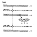
- An image sensor wafer 100 in which a plurality of image sensor chips 20 formed by wafer processing is disposed in a matrix form, is provided as shown in Fig. 3. And an IR filter glass 101 in the same shape as the wafer is provided. Also, a first lens array 102, which is formed by integrating a plurality of the first lenses 10 each having equivalent shape and size to the image sensor chip 20, is provided. Also, a second lens array 103, which is formed by integrating a plurality of the second lenses 30 each having equivalent shape and size to the image sensor chip 20, is provided. An iris film 104 having a shape of the wafer is also provided.
- the image sensor wafer 100, the IR filter glass 101, the first lens array 102, the second lens array 103 and the iris film 104 are bonded together, forming an integrated structure.
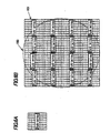
- Fig. 4A is a plan view showing a first example of the first lens array 102.
- the first example of the first lens array 102 has a multitude of the first lenses 10 arranged to make an envelope of the array in a shape essentially same as the wafer, as shown in Fig. 4A.
- the first lens array 102 is bonded onto the image sensor wafer 100, as shown in Fig. 4B.
- Fig. 5A is a plan view showing a second example of the first lens array 102.
- the second example of the first lens array 102 is composed of two kinds of sub-arrays, i.e., sub-arrays A and sub-arrays B, each of the sub-arrays being nearly triangular shaped, as shown in Fig. 5A.
- Four each of the sub-array A and the sub-array B are bonded to the image sensor wafer 100, as shown in Fig. 5B.
- Fig. 6A is a plan view showing a third example of the first lens array 102.
- the third example of the first lens array 102 is composed of a single kind of rectangular sub-arrays, as shown in Fig. 6A.
- the third example of the first lens array 102 has an advantage of manufacturing simplicity, since it is composed of a single kind of sub-arrays.
- the second lens array 103 is formed in the same way as the first lens array 102.
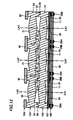
- Fig. 7 is a cross-sectional view of the integrated structure formed by bonding the image sensor wafer 100, the IR filter glass 101, the first lens array 102, the second lens array 103 and the iris film 104 together.
- the first lens frame 12 of the first lens array 102 is disposed across a border between two neighboring image sensor chips 20, in a way that a center line of the first lens frame 12 approximately coincides with the border, as shown in the figure.
- the second lens frame 32 of the second lens array 103 is bonded to a top surface of the first lens frame 12.
- the integrated structure described above is divided into individual camera modules 200 by cutting along borders between the image sensor chips 20 with a dicing blade or a laser, as shown in Fig. 8.
- the first lens frame 12 and the second lens frame 32 are divided into approximately half in width at the same time.
- each of the individual camera modules 200 is mounted on a printed circuit board through bump electrodes 25A and 25B on the back surface of the image sensor chip 20.
- first lens 10 and the second lens 30 are made of plastic, heat resistance of the plastic comes into question, because heat treatment is applied on the bump electrodes 25A and 25B usually when the camera module 200 is mounted on the printed circuit board. In this case, it is better to use a plastic material with a higher heat resistance or gold bumps which can be connected at lower temperature.
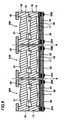
- a first lens 10 and a second lens 30 are bonded with an adhesive at a first lens frame 12 and a second lens frame 32 respectively, as described in the first embodiment.
- concave portions 13 for guide in the first lens frames 12 and convex portions 33 for guide in the second lens frames 32 are formed in advance, so that when bonding the first lens array 102 to the second lens array 103 the concave portions 13 for guide fit with the convex portions 33 for guide to prevent the misalignment in direction parallel to the bonding plane (horizontal direction in Fig. 7), as shown in Fig. 9. Alignment between the optical axis LA1 of the first lens body 11 and the optical axis LA2 of the second lens body 31 is thereby made easier than in the first embodiment.
- the convex portions for guide may be formed in the first lens frame 12 while the concave portions for guide are formed in the second lens frame 32 on the contrary to above description.
- the second lens array 103 is bonded to the first lens array 102 and an iris film 104 is bonded to the second lens array 103 as shown in Fig. 10, forming an integrated structure.
- the integrated structure described above is divided into individual camera modules 200 by cutting along borders between image sensor chips 20 with a dicing blade or a laser, as shown in Fig. 11.
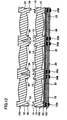
- ditches 34 to absorb the error in dimension are formed in the bonding surfaces of the second lens frames 32, as shown in Fig. 12. Depth of the ditches 34 is less than thickness of the second lens frame 32.
- the ditches may be formed by cutting the second lens frames 32 with a dicing apparatus.
- each of the concave portions 13 for guide fits exactly with each of the convex portions 33 for guide. As a result, it becomes easy to make the optical axis LA1 of the first lens body 11 coincide with the optical axis LA2 of the second lens body 31 in all of the camera modules 200.
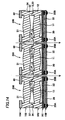
- the second lens array 103 is bonded to the first lens array 102 and an iris film 104 is bonded to the second lens array 103 as shown in Fig. 13, forming an integrated structure.
- the integrated structure described above is divided into individual camera modules 200 by cutting along borders between image sensor chips 20 with a dicing blade or a laser, as shown in Fig. 14.
- the camera module for a portable device is miniaturized to a size of the image sensor chip as well as its manufacturing cost is substantially reduced according to this invention.
- the camera module is capable of high quality picture of 300,000 pixels or above, since it has a compound lens.
Landscapes
- Engineering & Computer Science (AREA)
- Multimedia (AREA)
- Signal Processing (AREA)
- Physics & Mathematics (AREA)
- General Physics & Mathematics (AREA)
- Chemical & Material Sciences (AREA)
- Analytical Chemistry (AREA)
- Solid State Image Pick-Up Elements (AREA)
- Transforming Light Signals Into Electric Signals (AREA)
- Studio Devices (AREA)
- Lens Barrels (AREA)
Abstract
A camera module for a mobile device is reduced in size and
manufacturing cost. A first lens (10) is bonded to a surface
of an image sensor chip (20) through an IR filter. A
second lens (30) is bonded onto the first lens (10) forming
a compound lens. In addition, an iris material (40) is
bonded onto the second lens (30). Bump electrodes (25A, B),
which are external connection terminals, are formed on a
back surface of the image sensor chip (20) and connected to
a printed circuit board.
Description
- This invention relates to a camera module and its manufacturing method, specifically to a small size camera module suitable to be incorporated into a portable device such as a mobile phone and a manufacturing method of it.
- A mobile phone with camera function has come into widespread use in recent years. This type of mobile phone incorporates a small size camera module. Fig. 15 is a cross-sectional view showing a structure of such a camera module.
- Fig. 15 shows a lens-
barrel 50, alens 51 mounted inside the lens-barrel 50 and anIR filter 52 to block infrared radiation attached to a mouth of the lens-barrel 50. It also shows animage sensor chip 60 housed in a space within the lens-barrel 50 and electrically connected with a printedcircuit board 70. - The
image sensor chip 60 converts light incident on it from a photogenic subject through theIR filter 52 and thelens 51 into electric signals. In theimage sensor chip 60, CCDs (Charge Coupled Devices) are formed in a surface of asilicon chip 61 and a supportingglass substrate 62 is bonded to thesilicon chip 61 to bolster it. - Each of
redistribution wirings electrode pads image sensor chip 60, over a side surface and to a back surface of thesilicon chip 61. - Each of the
redistribution wirings glass substrate 65 which is bonded to the back surface of thesilicon chip 61. Each ofbump electrodes redistribution wirings glass substrate 65. Thebump electrodes circuit board 70. - A DSP (Digital Signal Processor) 80, which performs video signal processing on the electric signals from the
image sensor chip 60, is connected to a back surface of the printedcircuit board 70 throughbump electrodes - In the camera module described above, the lens-
barrel 50, thelens 51, theIR filter 52 and theimage sensor chip 60 are discrete components, and the camera module is assembled by putting these discrete components together. This causes difficulty in reducing the size and manufacturing cost of the camera module. - In addition, a combined use of a plurality of lenses needed to meet requirements of high quality picture further increases the size and manufacturing cost of the camera module.
- It is an object of this invention to lessen this drawback.
- The solution according to the invention lies in the features of the independent claims and preferably in those of the dependent claims.
- The invention provides a camera module that includes an image sensor unit having an image sensor chip that has a photoelectronic transducer disposed in its top surface and a terminal for external connection disposed on its back surface, a first lens bonded to the top surface of the image sensor unit, and a second lens bonded onto the first lens.
- The invention also provides a manufacturing method of a camera module. The method includes providing an image sensor wafer having a plurality of image sensor chips. Each of the image sensor chips has a photoelectronic transducer disposed in the top surface thereof and a terminal for external connection disposed on the back surface thereof. The method also includes providing a first lens array having a plurality of first lenses and a second lens array having a plurality of second lenses, bonding the image sensor wafer, the first lens array and the second lens array to form a bonded unit, and dividing the bonded unit into individual camera modules so that each of the camera modules includes one of the image sensor chips, one of the first lenses and one of the second lenses.
- By virtue of the invention camera modules having a compound lens (two or more lenses) are provided that allow for an increased picture quality combined with a cost effective manufacturing.
-
- Fig. 1 is a plan view showing a camera module according to a first embodiment of this invention.
- Fig. 2 is a cross-sectional view showing a section X-X in Fig. 1.
- Fig. 3 is a cross-sectional view showing a manufacturing method of the camera module according the first embodiment of this invention.
- Figs. 4A and 4B are plan views showing a first example of a lens array.
- Figs. 5A and 5B are plan views showing a second example of the lens array.
- Figs. 6A and 6B are plan views showing a third example of the lens array.
- Fig. 7 is a cross-sectional view showing a manufacturing method of the camera module according the first embodiment of this invention.
- Fig. 8 is a cross-sectional view showing the manufacturing method of the camera module according the first embodiment of this invention.
- Fig. 9 is a cross-sectional view showing a manufacturing method of a camera module according a second embodiment of this invention.
- Fig. 10 is a cross-sectional view showing the manufacturing method of the camera module according the second embodiment of this invention.
- Fig. 11 is a cross-sectional view showing the manufacturing method of the camera module according the second embodiment of this invention.
- Fig. 12 is a cross-sectional view showing a manufacturing method of a camera module according a third embodiment of this invention.
- Fig. 13 is a cross-sectional view showing the manufacturing method of the camera module according the third embodiment of this invention.
- Fig. 14 is a cross-sectional view showing the manufacturing method of the camera module according the third embodiment of this invention.
- Fig. 15 is a cross-sectional view showing a conventional camera module.
-
- Next, embodiments of this invention will be described in detail, referring to the figures.
- First, a structure of a camera module according to a first embodiment of this invention will be described. Fig. 1 is a plan view showing the camera module, and Fig. 2 is a cross-sectional view showing a section X-X in Fig. 1.
- Basic structure of the camera module is an integrated unit composed of an
image sensor chip 20, afirst lens 10 bonded onto theimage sensor chip 20 and asecond lens 30 bonded to thefirst lens 20 so that the two lenses face to each other. In addition, aniris material 40 made of a film such as an acrylic film or a polyolefin film is bonded to thesecond lens 30. Also, anIR filter 45 is bonded between theimage sensor chip 20 and thefirst lens 10. - The
first lens 10 is composed of afirst lens body 11 which is circular-shaped on the plan view and afirst lens frame 12 provided around thefirst lens body 11 to bolster it and molded together with thefirst lens body 11. Thesecond lens 30 is composed of asecond lens body 31 which is circular-shaped on the plan view and asecond lens frame 32 provided around thesecond lens body 31 to bolster it and molded together with thesecond lens body 31. - A surface of the
first lens frame 12 is bonded to a peripheral surface of theimage sensor chip 20 through theIR filter 45 using an adhesive. The other surface of thefirst lens frame 12 is bonded to thesecond lens frame 32 using an adhesive. - The
first lens body 11 and thesecond lens body 31 have predetermined shape of curved surface in order to obtain desired optical characteristics. Heights of thefirst lens frame 12 and thesecond lens frame 32 are determined to place centers (indicated by alternate long and short dashed lines in Fig. 2) of thefirst lens body 11 and thesecond lens body 32 at predetermined distances h1 and h2 from the surface of theimage sensor chip 20, respectively. - In the
image sensor chip 20, CCDs, which are photoelectronic transducers, are formed in a surface of asilicon chip 21, and a supportingglass substrate 22 is bonded to thesilicon chip 21 using an adhesive or the like to bolster thesilicon chip 21 which is as thin as several hundred micrometers.Electrode pads silicon chip 21. Each of theelectrode pads image sensor chip 20. - A bottom surface of each of the
electrode pads redistribution wirings silicon chip 21 to reach a back surface of theimage sensor chip 20. Each ofbump electrodes redistribution wirings - Although the
IR filter 45 is bonded between theimage sensor chip 20 and thefirst lens 10 in the structure described above, the IR filter may be bonded onto thesecond lens frame 32 of thesecond lens 30. In this case, theiris material 40 is formed on theIR filter 45. And thefirst lens 10 is bonded onto theimage sensor chip 20 directly. - When filtering function is given to the supporting
glass substrate 22 which bolsters thesilicon chip 21, theIR filter 45 can be omitted, leading to cost reduction due to reduction in number of parts. In this case, the filtering function is obtained by vacuum deposition of metal on the supportingglass substrate 22 or incorporating copper particles into the supportingglass substrate 22. - Next, a manufacturing method of the camera module described above will be explained. An
image sensor wafer 100, in which a plurality of image sensor chips 20 formed by wafer processing is disposed in a matrix form, is provided as shown in Fig. 3. And anIR filter glass 101 in the same shape as the wafer is provided. Also, afirst lens array 102, which is formed by integrating a plurality of thefirst lenses 10 each having equivalent shape and size to theimage sensor chip 20, is provided. Also, asecond lens array 103, which is formed by integrating a plurality of thesecond lenses 30 each having equivalent shape and size to theimage sensor chip 20, is provided. Aniris film 104 having a shape of the wafer is also provided. - Then the
image sensor wafer 100, theIR filter glass 101, thefirst lens array 102, thesecond lens array 103 and theiris film 104 are bonded together, forming an integrated structure. - Fig. 4A is a plan view showing a first example of the
first lens array 102. The first example of thefirst lens array 102 has a multitude of thefirst lenses 10 arranged to make an envelope of the array in a shape essentially same as the wafer, as shown in Fig. 4A. And thefirst lens array 102 is bonded onto theimage sensor wafer 100, as shown in Fig. 4B. - Fig. 5A is a plan view showing a second example of the
first lens array 102. The second example of thefirst lens array 102 is composed of two kinds of sub-arrays, i.e., sub-arrays A and sub-arrays B, each of the sub-arrays being nearly triangular shaped, as shown in Fig. 5A. Four each of the sub-array A and the sub-array B are bonded to theimage sensor wafer 100, as shown in Fig. 5B. - Fig. 6A is a plan view showing a third example of the
first lens array 102. The third example of thefirst lens array 102 is composed of a single kind of rectangular sub-arrays, as shown in Fig. 6A. - Sixteen sub-arrays are bonded to the
image sensor wafer 100, as shown in Fig. 6B. Although portions which fall off theimage sensor wafer 100 are used in vain, the third example of thefirst lens array 102 has an advantage of manufacturing simplicity, since it is composed of a single kind of sub-arrays. - The
second lens array 103 is formed in the same way as thefirst lens array 102. - Fig. 7 is a cross-sectional view of the integrated structure formed by bonding the
image sensor wafer 100, theIR filter glass 101, thefirst lens array 102, thesecond lens array 103 and theiris film 104 together. Thefirst lens frame 12 of thefirst lens array 102 is disposed across a border between two neighboring image sensor chips 20, in a way that a center line of thefirst lens frame 12 approximately coincides with the border, as shown in the figure. Thesecond lens frame 32 of thesecond lens array 103 is bonded to a top surface of thefirst lens frame 12. - After the bonding process described above, the integrated structure described above is divided into
individual camera modules 200 by cutting along borders between theimage sensor chips 20 with a dicing blade or a laser, as shown in Fig. 8. Thefirst lens frame 12 and thesecond lens frame 32 are divided into approximately half in width at the same time. - Then each of the
individual camera modules 200 is mounted on a printed circuit board throughbump electrodes image sensor chip 20. - When the
first lens 10 and thesecond lens 30 are made of plastic, heat resistance of the plastic comes into question, because heat treatment is applied on thebump electrodes camera module 200 is mounted on the printed circuit board. In this case, it is better to use a plastic material with a higher heat resistance or gold bumps which can be connected at lower temperature. - Next, a second embodiment of this invention will be explained referring to Fig. 9, Fig. 10 and Fig. 11. A
first lens 10 and asecond lens 30 are bonded with an adhesive at afirst lens frame 12 and asecond lens frame 32 respectively, as described in the first embodiment. - When there arises an alignment error in a direction parallel to a bonding plane (horizontal direction in Fig. 7) in bonding a
second lens array 103 to afirst lens array 102 which is bonded onto animage sensor 100, an optical axis LA1 of afirst lens body 11 and an optical axis LA2 of asecond lens body 31 are misaligned and desired optical characteristics as a compound lens are not obtained. - Thus in this embodiment,
concave portions 13 for guide in the first lens frames 12 andconvex portions 33 for guide in the second lens frames 32 are formed in advance, so that when bonding thefirst lens array 102 to thesecond lens array 103 theconcave portions 13 for guide fit with theconvex portions 33 for guide to prevent the misalignment in direction parallel to the bonding plane (horizontal direction in Fig. 7), as shown in Fig. 9. Alignment between the optical axis LA1 of thefirst lens body 11 and the optical axis LA2 of thesecond lens body 31 is thereby made easier than in the first embodiment. Note that the convex portions for guide may be formed in thefirst lens frame 12 while the concave portions for guide are formed in thesecond lens frame 32 on the contrary to above description. - After that, the
second lens array 103 is bonded to thefirst lens array 102 and aniris film 104 is bonded to thesecond lens array 103 as shown in Fig. 10, forming an integrated structure. Then, the integrated structure described above is divided intoindividual camera modules 200 by cutting along borders betweenimage sensor chips 20 with a dicing blade or a laser, as shown in Fig. 11. - Next, a third embodiment of this invention will be explained referring to Fig. 12, Fig. 13 and Fig. 14. Alignment between the optical axis of the
first lens body 11 and the optical axis of thesecond lens body 31 is made easier in the second embodiment described above than in the first embodiment. However, in injection molding of thefirst lens array 102 and thesecond lens array 103, there arises an error in dimension in each of the lens arrays. As a result, it becomes difficult to make the optical axis LA1 of thefirst lens body 11 coincide with the optical axis LA2 of thesecond lens body 31 in all of thecamera modules 200. - That is, when bonding the
second lens array 103 to thefirst lens array 102 withconcave portions 13 for guide in thefirst lens frame 12 and theconvex portions 33 for guide in thesecond lens frame 32 formed in advance as described above, even if theconcave portion 13 for guide exactly fits with theconvex portion 33 for guide in a certain location (for example, at an edge of the lens arrays), the error in dimension grows cumulatively as distance from the certain location increases, leading to a poor fit between theconcave portion 13 for guide and theconvex portion 33 for guide. - Thus in this embodiment, allowing for a certain extent of error in dimension in molding the
first lens array 102 and thesecond lens array 103, ditches 34 to absorb the error in dimension are formed in the bonding surfaces of the second lens frames 32, as shown in Fig. 12. Depth of theditches 34 is less than thickness of thesecond lens frame 32. The ditches may be formed by cutting the second lens frames 32 with a dicing apparatus. - With resiliently varying width of the
ditches 34 to absorb the error in dimension when bonding thesecond lens array 103 to thefirst lens array 102, each of theconcave portions 13 for guide fits exactly with each of theconvex portions 33 for guide. As a result, it becomes easy to make the optical axis LA1 of thefirst lens body 11 coincide with the optical axis LA2 of thesecond lens body 31 in all of thecamera modules 200. - After that, the
second lens array 103 is bonded to thefirst lens array 102 and aniris film 104 is bonded to thesecond lens array 103 as shown in Fig. 13, forming an integrated structure. Then, the integrated structure described above is divided intoindividual camera modules 200 by cutting along borders betweenimage sensor chips 20 with a dicing blade or a laser, as shown in Fig. 14. - The camera module for a portable device is miniaturized to a size of the image sensor chip as well as its manufacturing cost is substantially reduced according to this invention. The camera module is capable of high quality picture of 300,000 pixels or above, since it has a compound lens.
Claims (15)
- A camera module comprising:an image sensor unit comprising an image sensor chip (20) that has a photoelectronic transducer disposed in a top surface of the image sensor chip (20) and a terminal (25A, B) for external connection disposed on a back surface of the image sensor chip (20);a first lens (10) bonded to a top surface of the image sensor unit; anda second lens (30) bonded onto the first lens (10).
- The camera module of claim 1, wherein the first and second lenses (10, 30) are configured to support weights thereof without a support of lens barrel.
- The camera module of claim 1 or 2, wherein the first lens (10) comprises a first lens body (11) and a first lens frame (12) to support the first lens body (11), the second lens (30) comprises a second lens body (31) and a second lens frame (32) to support the second lens body (31), and a surface of the first lens frame (12) is bonded onto the image sensor unit and another surface of the first lens frame (12) is bonded to a surface of the second lens frame (32).
- The camera module of claim 3, wherein a height of the first lens frame (12) and a height of the second lens frame (32) are determined so that the first lens body (11) and the second lens body (31) are placed at predetermined distances respectively from the top surface of the image sensor chip (20).
- The camera module of claim 3 or 4, further comprising a first guide (13) formed in the first lens frame (12) and a second guide (33) formed in the second lens frame (32), wherein the first guide (13) engages with the second guide (33).
- The camera module of claim 5, further comprising a ditch (34) formed in the surface of the second lens frame (32).
- The camera module according to any of claims 1 to 6, further comprising a filter (45) to block light within a predetermined range of wavelength.
- The camera module according to any of claims 1 to 7, further comprising an iris (40) to limit light incident on the image sensor chip (20).
- A manufacturing method of a camera module comprising:providing an image sensor wafer (100) comprising a plurality of image sensor chips (20), each of the image sensor chips (20) comprising a photoelectronic transducer disposed in a top surface thereof and a terminal for external connection (25A, B) disposed on a back surface thereof;providing a first lens array (102) comprising a plurality of first lenses (10) and a second lens (103) array comprising a plurality of second lenses (30);bonding the image sensor wafer (100), the first lens array (102) and the second lens array (103) to form a bonded unit; anddividing the bonded unit into individual camera modules (200) so that each of the camera modules (200) includes one of the image sensor chips (20), one of the first lenses (10) and one of the second lenses (30).
- The manufacturing method of claim 9, wherein each of the first lenses (10) comprises a first lens body (11) and a first lens frame (12) to support the first lens body (11), each of the second lenses (30) comprises a second lens body (31) and a second lens frame (32) to support the second lens body (31), and a surface of the first lens frame (12) is bonded to a surface of the second lens frame (32).
- The manufacturing method of claim 10, further comprising forming a first guide (13) in the first lens frame (12) and forming a second guide (33) in the second lens frame (32), wherein the first and second lens arrays (102, 103) are aligned by engaging the first guide (13) with the second guide (33).
- The manufacturing method of claim 11, further comprising forming a ditch (34) for the alignment in the surface of the second lens frame (32) before the alignment.
- The manufacturing method according to any of claims 9 to 12, wherein each of the first lens array (102) and the second lens array (103) is formed in a horizontal shape substantially the a same as the image sensor wafer (100).
- The manufacturing method according to any of claims 9 to 13, wherein each of the first lens array (102) and the second lens array (103) comprises a plurality of individual sub arrays of at least two different kinds.
- The manufacturing method according to any of claims 9 to 13, wherein each of the first lens array (102) and the second lens (103) array comprises a plural of rectangular sub arrays.
Applications Claiming Priority (2)
| Application Number | Priority Date | Filing Date | Title |
|---|---|---|---|
| JP2003017012 | 2003-01-27 | ||
| JP2003017012A JP2004226872A (en) | 2003-01-27 | 2003-01-27 | Camera module and manufacturing method thereof |
Publications (1)
| Publication Number | Publication Date |
|---|---|
| EP1443754A2 true EP1443754A2 (en) | 2004-08-04 |
Family
ID=32652826
Family Applications (1)
| Application Number | Title | Priority Date | Filing Date |
|---|---|---|---|
| EP04001675A Withdrawn EP1443754A2 (en) | 2003-01-27 | 2004-01-27 | Camera module and manufacturing method thereof |
Country Status (6)
| Country | Link |
|---|---|
| US (1) | US20040212719A1 (en) |
| EP (1) | EP1443754A2 (en) |
| JP (1) | JP2004226872A (en) |
| KR (1) | KR20040068865A (en) |
| CN (1) | CN1517736A (en) |
| TW (1) | TW200421863A (en) |
Cited By (16)
| Publication number | Priority date | Publication date | Assignee | Title |
|---|---|---|---|---|
| FR2936098A1 (en) * | 2008-08-25 | 2010-03-19 | Cheng Uei Prec Ind Co Ltd | Camera module for e.g. mobile phone, has frame having supporting portion and bearing portion extending inward from supporting portion for supporting infrared-cut transparent cover of lower lens unit |
| EP2259096A1 (en) * | 2009-06-03 | 2010-12-08 | Samsung Electronics Co., Ltd. | Wafer-level lens module and image pickup module including the same |
| US8120858B2 (en) | 2008-12-04 | 2012-02-21 | Samsung Electronics Co., Ltd. | Micro lens, method and apparatus for manufacturing micro lens, and camera module including micro lens |
| US8305699B2 (en) | 2009-09-23 | 2012-11-06 | Samsung Electronics Co., Ltd. | Wafer-level lens module with extended depth of field and imaging device including the wafer-level lens module |
| US8456560B2 (en) | 2007-01-26 | 2013-06-04 | Digitaloptics Corporation | Wafer level camera module and method of manufacture |
| US8475061B2 (en) | 2008-01-16 | 2013-07-02 | Omnivision Technologies, Inc. | Membrane suspended optical elements, and associated methods |
| US8520137B2 (en) | 2009-08-13 | 2013-08-27 | Samsung Electronics Co., Ltd. | Wafer-level lens module and image pickup device including the same |
| US8605208B2 (en) | 2007-04-24 | 2013-12-10 | Digitaloptics Corporation | Small form factor modules using wafer level optics with bottom cavity and flip-chip assembly |
| US8885272B2 (en) | 2011-05-03 | 2014-11-11 | Omnivision Technologies, Inc. | Flexible membrane and lens assembly and associated method of lens replication |
| US9419032B2 (en) | 2009-08-14 | 2016-08-16 | Nanchang O-Film Optoelectronics Technology Ltd | Wafer level camera module with molded housing and method of manufacturing |
| EP2298543A3 (en) * | 2009-09-17 | 2016-09-07 | FUJIFILM Corporation | Master model of lens array and method of manufacturing the same |
| EP2298544A3 (en) * | 2009-09-16 | 2016-10-05 | FUJIFILM Corporation | Wafer-level lens array, method of manufacturing wafer-level lens array, lens module and imaging unit |
| EP3037852A4 (en) * | 2013-08-20 | 2017-03-22 | Daicel Corporation | Wafer lens, wafer lens array, wafer lens laminate, and wafer lens array laminate |
| DE102015226173A1 (en) * | 2015-12-21 | 2017-06-22 | Robert Bosch Gmbh | Optical imaging system with a deformable due to electrical and / or magnetic forces lens |
| WO2019044540A1 (en) * | 2017-08-31 | 2019-03-07 | Sony Semiconductor Solutions Corporation | Imaging apparatus and electronic apparatus |
| US12379567B2 (en) | 2019-12-25 | 2025-08-05 | Seikoh Giken Co., Ltd. | Lens unit |
Families Citing this family (51)
| Publication number | Priority date | Publication date | Assignee | Title |
|---|---|---|---|---|
| KR100547745B1 (en) * | 2003-10-23 | 2006-01-31 | 삼성전자주식회사 | Image sensor module and assembly method of camera device |
| KR100649490B1 (en) * | 2004-06-14 | 2006-11-24 | 삼성전기주식회사 | Camera module for camera phone |
| JP4349232B2 (en) * | 2004-07-30 | 2009-10-21 | ソニー株式会社 | Semiconductor module and MOS solid-state imaging device |
| JP4379295B2 (en) * | 2004-10-26 | 2009-12-09 | ソニー株式会社 | Semiconductor image sensor module and manufacturing method thereof |
| KR100691184B1 (en) * | 2005-06-28 | 2007-03-09 | 삼성전기주식회사 | Adhesion Method for Lamination of Wafer Scale Lenses and Wafer Scale Lenses Produced thereby |
| JP4585409B2 (en) * | 2005-08-24 | 2010-11-24 | 株式会社東芝 | Small camera module |
| KR100652551B1 (en) | 2005-11-07 | 2006-12-01 | 삼성전기주식회사 | Small camera module and manufacturing method |
| US7973380B2 (en) * | 2005-11-23 | 2011-07-05 | Taiwan Semiconductor Manufacturing Company, Ltd. | Method for providing metal extension in backside illuminated sensor for wafer level testing |
| KR100744925B1 (en) * | 2005-12-27 | 2007-08-01 | 삼성전기주식회사 | Camera module package |
| CN100405107C (en) * | 2006-01-06 | 2008-07-23 | 林颖诚 | Mobile phone camera module filter and manufacturing method thereof |
| JP2007221231A (en) * | 2006-02-14 | 2007-08-30 | Denso Corp | Imaging module and manufacturing method thereof |
| KR101210039B1 (en) * | 2006-03-13 | 2012-12-07 | 엘지이노텍 주식회사 | Camera module |
| US20070236591A1 (en) * | 2006-04-11 | 2007-10-11 | Tam Samuel W | Method for mounting protective covers over image capture devices and devices manufactured thereby |
| EP2104877A4 (en) * | 2006-09-14 | 2010-02-24 | Tessera Tech Hungary Kft | Imaging system with improved image quality and associated methods |
| WO2008087485A2 (en) * | 2006-09-14 | 2008-07-24 | Tessera Technologies Hungary Kft. | Imaging system with relaxed assembly tolerances and associated methods |
| WO2008133946A1 (en) * | 2007-04-24 | 2008-11-06 | Flextronics Ap Llc | Auto focus/ zoom modules using wafer level optics |
| US7825985B2 (en) * | 2007-07-19 | 2010-11-02 | Flextronics Ap, Llc | Camera module back-focal length adjustment method and ultra compact components packaging |
| JP5026198B2 (en) * | 2007-08-28 | 2012-09-12 | 日立マクセル株式会社 | Lens unit, lens module, camera module, and method for manufacturing camera module mounted circuit board |
| JP4799543B2 (en) * | 2007-12-27 | 2011-10-26 | 株式会社東芝 | Semiconductor package and camera module |
| US9118825B2 (en) | 2008-02-22 | 2015-08-25 | Nan Chang O-Film Optoelectronics Technology Ltd. | Attachment of wafer level optics |
| JP4966931B2 (en) | 2008-08-26 | 2012-07-04 | シャープ株式会社 | Electronic element wafer module and manufacturing method thereof, electronic element module and manufacturing method thereof, electronic information device |
| JP4764941B2 (en) * | 2008-09-25 | 2011-09-07 | シャープ株式会社 | Optical element, optical element wafer, optical element wafer module, optical element module, optical element module manufacturing method, electronic element wafer module, electronic element module manufacturing method, electronic element module, and electronic information device |
| WO2010038554A1 (en) * | 2008-09-30 | 2010-04-08 | コニカミノルタオプト株式会社 | Method for manufacturing optical component, lens, lens unit and camera module |
| JP4832500B2 (en) * | 2008-12-01 | 2011-12-07 | シャープ株式会社 | Method for manufacturing electronic element wafer module and method for manufacturing optical element wafer module |
| JP5254139B2 (en) * | 2009-07-03 | 2013-08-07 | シャープ株式会社 | Multilayer lens, laminated wafer lens, and manufacturing method thereof |
| JP5345455B2 (en) * | 2009-07-03 | 2013-11-20 | シャープ株式会社 | Multilayer lens, laminated wafer lens, and manufacturing method thereof |
| JP5450633B2 (en) * | 2009-09-09 | 2014-03-26 | 株式会社東芝 | Solid-state imaging device and manufacturing method thereof |
| JP5572355B2 (en) | 2009-09-30 | 2014-08-13 | 富士フイルム株式会社 | Lens array and lens array laminate |
| JP5448685B2 (en) * | 2009-09-30 | 2014-03-19 | 富士フイルム株式会社 | Element array, element array laminate, and method for manufacturing element array laminate |
| CN102045494A (en) * | 2009-10-22 | 2011-05-04 | 国碁电子(中山)有限公司 | Camera module and making method thereof |
| KR101646808B1 (en) * | 2009-10-28 | 2016-08-08 | 가부시키가이샤 제이올레드 | Lens sheet, display panel device, and display device |
| TWM382505U (en) * | 2010-01-15 | 2010-06-11 | Cheng Uei Prec Ind Co Ltd | Video device |
| JP2011209699A (en) * | 2010-03-10 | 2011-10-20 | Fujifilm Corp | Wafer lens array and method for manufacturing the same |
| EP2369371A3 (en) * | 2010-03-10 | 2013-05-01 | Fujifilm Corporation | Wafer lens array and method for manufacturing the same |
| US9910239B2 (en) * | 2010-11-30 | 2018-03-06 | Flir Systems Trading Belgium Bvba | Wafer level optical elements and applications thereof |
| JP5540120B2 (en) * | 2011-01-21 | 2014-07-02 | 富士フイルム株式会社 | Stacked lens array and lens module |
| WO2012161802A2 (en) | 2011-02-24 | 2012-11-29 | Flextronics Ap, Llc | Autofocus camera module packaging with circuitry-integrated actuator system |
| US8545114B2 (en) | 2011-03-11 | 2013-10-01 | Digitaloptics Corporation | Auto focus-zoom actuator or camera module contamination reduction feature with integrated protective membrane |
| TWI461742B (en) * | 2012-01-09 | 2014-11-21 | Largan Precision Co Ltd | Multiple-layered lens array assembly |
| CN102903726B (en) * | 2012-09-29 | 2016-02-10 | 格科微电子(上海)有限公司 | The wafer-level packaging method of imageing sensor |
| WO2014102167A1 (en) * | 2012-12-28 | 2014-07-03 | Umicore | Frontal aperture stop for ir optics |
| US9923008B2 (en) | 2013-04-12 | 2018-03-20 | Omnivision Technologies, Inc. | Wafer-level array cameras and methods for fabricating the same |
| US9088705B1 (en) | 2013-08-30 | 2015-07-21 | Amazon Technologies, Inc. | Camera module package with stiffener-mounted image sensor die |
| US9241097B1 (en) | 2013-09-27 | 2016-01-19 | Amazon Technologies, Inc. | Camera module including image sensor die in molded cavity substrate |
| US10095086B2 (en) * | 2013-12-23 | 2018-10-09 | Lg Electronics Inc. | Camera module |
| JP6967830B2 (en) * | 2015-07-31 | 2021-11-17 | ソニーセミコンダクタソリューションズ株式会社 | Semiconductor devices, lens modules and their manufacturing methods, and electronic devices |
| US10488632B2 (en) * | 2016-01-20 | 2019-11-26 | Mems Optical Zoom Corporation | MEMS lens actuator |
| US10466501B2 (en) * | 2016-05-26 | 2019-11-05 | Ams Sensors Singapore Pte. Ltd. | Optoelectronic modules including an optical system tilted with respect to a focal plane |
| US10925160B1 (en) | 2016-06-28 | 2021-02-16 | Amazon Technologies, Inc. | Electronic device with a display assembly and silicon circuit board substrate |
| JP6976751B2 (en) * | 2017-07-06 | 2021-12-08 | ソニーセミコンダクタソリューションズ株式会社 | Image pickup device, manufacturing method of image pickup device, and electronic equipment |
| CN112217964A (en) * | 2019-07-11 | 2021-01-12 | 南昌欧菲光电技术有限公司 | Support, camera module and electronic equipment terminal |
-
2003
- 2003-01-27 JP JP2003017012A patent/JP2004226872A/en active Pending
- 2003-12-23 TW TW092136482A patent/TW200421863A/en unknown
-
2004
- 2004-01-20 CN CNA2004100028802A patent/CN1517736A/en active Pending
- 2004-01-26 KR KR1020040004581A patent/KR20040068865A/en not_active Ceased
- 2004-01-27 EP EP04001675A patent/EP1443754A2/en not_active Withdrawn
- 2004-02-05 US US10/771,509 patent/US20040212719A1/en not_active Abandoned
Cited By (19)
| Publication number | Priority date | Publication date | Assignee | Title |
|---|---|---|---|---|
| US8456560B2 (en) | 2007-01-26 | 2013-06-04 | Digitaloptics Corporation | Wafer level camera module and method of manufacture |
| US8605208B2 (en) | 2007-04-24 | 2013-12-10 | Digitaloptics Corporation | Small form factor modules using wafer level optics with bottom cavity and flip-chip assembly |
| EP2240805B1 (en) * | 2008-01-16 | 2014-02-26 | OmniVision CDM Optics, Inc. | Membrane suspended optical elements, and associated methods |
| US8475061B2 (en) | 2008-01-16 | 2013-07-02 | Omnivision Technologies, Inc. | Membrane suspended optical elements, and associated methods |
| DE102008046755A1 (en) * | 2008-08-25 | 2010-03-25 | Cheng Uei Precision Industry Co., Ltd., Tucheng | Camera module for e.g. mobile phone, has frame having supporting portion and bearing portion extending inward from supporting portion for supporting infrared-cut transparent cover of lower lens unit |
| FR2936098A1 (en) * | 2008-08-25 | 2010-03-19 | Cheng Uei Prec Ind Co Ltd | Camera module for e.g. mobile phone, has frame having supporting portion and bearing portion extending inward from supporting portion for supporting infrared-cut transparent cover of lower lens unit |
| US8120858B2 (en) | 2008-12-04 | 2012-02-21 | Samsung Electronics Co., Ltd. | Micro lens, method and apparatus for manufacturing micro lens, and camera module including micro lens |
| EP2193911A3 (en) * | 2008-12-04 | 2012-05-09 | Samsung Electronics Co., Ltd. | Micro lens, method and apparatus for manufacturing micro lens, and camera module including micro lens |
| EP2259096A1 (en) * | 2009-06-03 | 2010-12-08 | Samsung Electronics Co., Ltd. | Wafer-level lens module and image pickup module including the same |
| US8520137B2 (en) | 2009-08-13 | 2013-08-27 | Samsung Electronics Co., Ltd. | Wafer-level lens module and image pickup device including the same |
| US9419032B2 (en) | 2009-08-14 | 2016-08-16 | Nanchang O-Film Optoelectronics Technology Ltd | Wafer level camera module with molded housing and method of manufacturing |
| EP2298544A3 (en) * | 2009-09-16 | 2016-10-05 | FUJIFILM Corporation | Wafer-level lens array, method of manufacturing wafer-level lens array, lens module and imaging unit |
| EP2298543A3 (en) * | 2009-09-17 | 2016-09-07 | FUJIFILM Corporation | Master model of lens array and method of manufacturing the same |
| US8305699B2 (en) | 2009-09-23 | 2012-11-06 | Samsung Electronics Co., Ltd. | Wafer-level lens module with extended depth of field and imaging device including the wafer-level lens module |
| US8885272B2 (en) | 2011-05-03 | 2014-11-11 | Omnivision Technologies, Inc. | Flexible membrane and lens assembly and associated method of lens replication |
| EP3037852A4 (en) * | 2013-08-20 | 2017-03-22 | Daicel Corporation | Wafer lens, wafer lens array, wafer lens laminate, and wafer lens array laminate |
| DE102015226173A1 (en) * | 2015-12-21 | 2017-06-22 | Robert Bosch Gmbh | Optical imaging system with a deformable due to electrical and / or magnetic forces lens |
| WO2019044540A1 (en) * | 2017-08-31 | 2019-03-07 | Sony Semiconductor Solutions Corporation | Imaging apparatus and electronic apparatus |
| US12379567B2 (en) | 2019-12-25 | 2025-08-05 | Seikoh Giken Co., Ltd. | Lens unit |
Also Published As
| Publication number | Publication date |
|---|---|
| JP2004226872A (en) | 2004-08-12 |
| TW200421863A (en) | 2004-10-16 |
| CN1517736A (en) | 2004-08-04 |
| US20040212719A1 (en) | 2004-10-28 |
| KR20040068865A (en) | 2004-08-02 |
Similar Documents
| Publication | Publication Date | Title |
|---|---|---|
| US20040212719A1 (en) | Camera module and manufacturing method thereof | |
| US20040169763A1 (en) | Camera module and manufacturing method thereof | |
| US6853005B2 (en) | Camera module and manufacturing method thereof | |
| US7166907B2 (en) | Image sensor module with substrate and frame and method of making the same | |
| US7863702B2 (en) | Image sensor package and method of manufacturing the same | |
| CN101652695B (en) | Wafer level camera module and method of manufacture | |
| KR101442060B1 (en) | Camera module and imaging device | |
| US20070126912A1 (en) | Camera module and manufacturing method for such a camera module | |
| US20060164539A1 (en) | Camera module, camera system and method of manufacturing a camera module | |
| JP5035707B2 (en) | Imaging device manufacturing method and imaging device | |
| KR101032391B1 (en) | Electronic device wafer module, electronic device module, sensor wafer module, sensor module, lens array plate, sensor module manufacturing method and electronic information device | |
| US20100242269A1 (en) | Compact lens turret assembly | |
| JP2004229167A (en) | Manufacturing method of camera module | |
| US9111827B2 (en) | Manufacturing method of solid-state imaging apparatus, solid-state imaging apparatus, and electronic imaging apparatus | |
| JP2004233482A (en) | Method of manufacturing camera module | |
| JP4352664B2 (en) | Semiconductor device and manufacturing method thereof | |
| CN103081105A (en) | Image pickup device, image pickup module and camera | |
| KR100956381B1 (en) | Manufacturing Method of Wafer Level Camera Module | |
| US7202469B2 (en) | Solid-state imaging device with molded resin ribs and method of manufacturing | |
| JP2006294720A (en) | The camera module | |
| KR20100027857A (en) | Wafer level camera module and manufacturing method thereof | |
| JP2004233483A (en) | The camera module | |
| EP1713126A1 (en) | Image pickup device and a manufacturing method thereof | |
| JP2003243634A (en) | Solid-state imaging device and manufacturing method thereof | |
| JPH04172761A (en) | Contact type linear image sensor module |
Legal Events
| Date | Code | Title | Description |
|---|---|---|---|
| PUAI | Public reference made under article 153(3) epc to a published international application that has entered the european phase |
Free format text: ORIGINAL CODE: 0009012 |
|
| AK | Designated contracting states |
Kind code of ref document: A2 Designated state(s): AT BE BG CH CY CZ DE DK EE ES FI FR GB GR HU IE IT LI LU MC NL PT RO SE SI SK TR |
|
| AX | Request for extension of the european patent |
Extension state: AL LT LV MK |
|
| STAA | Information on the status of an ep patent application or granted ep patent |
Free format text: STATUS: THE APPLICATION IS DEEMED TO BE WITHDRAWN |
|
| 18D | Application deemed to be withdrawn |
Effective date: 20080801 |