EP1443644A2 - Simultaneous Gm-C filter and variable gain amplifier circuit - Google Patents
Simultaneous Gm-C filter and variable gain amplifier circuit Download PDFInfo
- Publication number
- EP1443644A2 EP1443644A2 EP03103735A EP03103735A EP1443644A2 EP 1443644 A2 EP1443644 A2 EP 1443644A2 EP 03103735 A EP03103735 A EP 03103735A EP 03103735 A EP03103735 A EP 03103735A EP 1443644 A2 EP1443644 A2 EP 1443644A2
- Authority
- EP
- European Patent Office
- Prior art keywords
- base band
- filter
- current consumption
- band system
- cells
- Prior art date
- Legal status (The legal status is an assumption and is not a legal conclusion. Google has not performed a legal analysis and makes no representation as to the accuracy of the status listed.)
- Withdrawn
Links
- 238000000034 method Methods 0.000 claims abstract description 13
- 238000001914 filtration Methods 0.000 claims description 7
- 230000003321 amplification Effects 0.000 claims description 5
- 238000003199 nucleic acid amplification method Methods 0.000 claims description 5
- 238000006243 chemical reaction Methods 0.000 abstract description 15
- 238000000638 solvent extraction Methods 0.000 abstract description 3
- 230000008901 benefit Effects 0.000 description 7
- 230000004044 response Effects 0.000 description 7
- 238000010586 diagram Methods 0.000 description 4
- 230000015572 biosynthetic process Effects 0.000 description 3
- 238000003786 synthesis reaction Methods 0.000 description 3
- 238000012986 modification Methods 0.000 description 2
- 230000004048 modification Effects 0.000 description 2
- 230000004075 alteration Effects 0.000 description 1
- 230000001413 cellular effect Effects 0.000 description 1
- 230000006835 compression Effects 0.000 description 1
- 238000007906 compression Methods 0.000 description 1
- 238000010276 construction Methods 0.000 description 1
- 238000006467 substitution reaction Methods 0.000 description 1
Images

Classifications
-
- H—ELECTRICITY
- H03—ELECTRONIC CIRCUITRY
- H03H—IMPEDANCE NETWORKS, e.g. RESONANT CIRCUITS; RESONATORS
- H03H11/00—Networks using active elements
- H03H11/02—Multiple-port networks
- H03H11/04—Frequency selective two-port networks
- H03H11/0422—Frequency selective two-port networks using transconductance amplifiers, e.g. gmC filters
- H03H11/0444—Simulation of ladder networks
- H03H11/045—Leapfrog structures
Definitions
- This invention relates generally to receiver systems, and more particularly to a system and method for reducing current consumption of direct conversion receivers and low IF receiver systems, among other things.
- Direct conversion receivers are gaining in popularity in modem receiver systems, especially for cellular phone applications. This structure has the advantage of not requiring any IF filters and reducing the number of down-conversions required. This advantageously minimizes cost, reduces PC board area and reduces die size.
- the current consumption of direct conversion receivers however, has typically been higher than that seen with heterodyne systems. This has hurt the competitiveness of direct conversion systems. Most of the additional current consumption is associated with the base band circuitry of a direct conversion receiver.
- the present invention is directed to a system and method for reducing the current consumption associated with modem receiver systems, such as direct conversion receivers and low IF receiver systems, among other things.
- the present invention provides various technical advantages. Since the base band system filter also performs the variable gain amplification (VGA) function, the current consumption of the VGA is eliminated. Further, since the gain partitioning of the filter structure is superior, the noise performance of the filter is greatly reduced; and the base band front end low noise amplifier (LNA) can be eliminated, also eliminating the current consumption of the base band LNA.
- VGA variable gain amplification
- LNA base band front end low noise amplifier
- a folded g m structure can be used to implement the filter g m stages, substantially cutting the current consumption of the base band filter by a factor of two.
- a receiver base band system comprises a Gm-C filter having a plurality of g m stages configured to provide an automatic gain control (AGC) function.
- AGC automatic gain control
- a receiver base band system comprises a filter having a plurality of current folded g m cells configured to provide a variable gain amplification (VGA) function.
- VGA variable gain amplification
- a receiver base band system comprises base band circuitry having base band filtering means for providing variable gain amplification of base band filter input signals.
- a method of reducing current consumption of a receiver base band system comprises the steps of providing a base band Gm-C filter having g m cells configured to provide mismatched forward and reverse g m values, and further configured to provide an AGC function; filtering an input signal via the base band Gm-C filter to provide a base band filtered output signal; and controlling g m values associated with the Gm-C filter to variably amplify the filtered output signal.
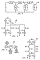
- Table 1 shows the current consumption associated with the base band portion of one known direct conversion receiver architecture suitable for WCDMA applications. A system and method of significantly reducing this current consumption according to particular embodiments of the present invention are described herein below with reference to Figures 1-5. The present invention is not so limited however, and it shall be understood that the techniques presented herein can just as easily be employed to reduce the current consumption of low IF receiver systems, among others.
- Equations 7 though 12 If a circuit can be synthesized to create the voltages defined by Equations 7 though 12, then the voltage V 6 ' will have the same frequency response as the ladder network 100 depicted in Figure 1, and will also have an additional voltage gain given by the product of a 1 through a 6 as seen by equation 12. This circuit synthesis can be achieved by first combining equations 1 through 6 with Equations 7 through 12 respectively, to yield equations 13 through 18 below.
- the present inventor found that such a circuit could be implemented using the Gm-C structure 200 shown in Figure 2 that illustrates a Gm-C filter with AGC function according to one embodiment of the present invention.
- the use of the circuit structure 200 shown in Figure 2 has several advantages. One of the most significant advantages is that the gain and filtering are apportioned much better than that achievable using more conventional circuit structures.
- FIG 3 is a simple block diagram illustrating one known base band architecture 300 that employs a low-pass filter 302 implemented as a unity gain g m -C filter having a plurality of g m stages.
- the present inventor realized that each of the g m stages within the filter 302 contribute roughly an equal amount to the input noise voltage.
- a base band LNA 304 was added to overcome this noise.
- the gain of the base band LNA 304 however, increases the linearity requirements on the filter 302 and VGA 306.
- the base-band LNA 304 is no longer required for the circuit 200 depicted in Figure 2 since at maximum gain, where the noise performance is most critical, all of the stages have significant gain and the stages after the first g m stage contribute a relatively minor amount to the input noise voltage. Eliminating the base band LNA 304 was found by the present inventor to have two advantages. First, the current consumption of the base band LNA 304 is eliminated; and second, the linearity requirement on the gm-C filter 302 is reduced.
- the present inventor also realized a further current consumption savings could be achieved by using the current folded structure 500 shown in Figure 5 for each g m cell discussed herein before.
- Those skilled in the filter synthesis art will readily appreciate the g m of the forward and feedback paths for a conventional unity gain g m -C filter must match.
- a conventional g m structure 400 shown in Figure 4 can be employed. Since the g m cells shown in Figure 2 have forward and reverse g m values that are not the same, it can be appreciated that the forward and feedback g m 's need not match. This allows the current consumption of the gm-C filter 302 to be cut in half.
- the structure 200 depicted in Figure 2 can be used to dramatically reduce the current consumption in direct conversion receivers due to three factors. 1) Since the filter 302 also performs the VGA function, the current consumption of the VGA 304 is eliminated; 2) Since the gain partitioning of the structure 200 depicted in Figure 2 is superior, the noise performance of the filter 302 is greatly reduced and the base band LNA 304 can be eliminated also eliminating the current consumption of the base band LNA 304; and 3) The folded g m structure 500 depicted in Figure 5 can be used, cutting the current consumption of the base band filter by a factor of two. The structure 200 shown in Figure 2 notably does require control circuitry to set the g m values of the forward and feedback paths independently.
- control circuitry Details of this control circuitry are not discussed herein to preserve clarity and brevity, and since those skilled in the direct conversion receiver system art will readily be able to employ a large variety of techniques to implement the control circuitry.
- the current consumption of this control circuitry will be substantially less than the current saved due to the three factors discussed herein above.
- the present inventor found that the base band circuitry current consumption (16.7 mA) shown in Table 1 could be reduced by about a factor or three to 5.5 mA, by implementing the structure 200 shown in Figure 2.
- Figure 6 shows a simulated frequency response 600 at various gain settings for a base band architecture that employs the Gm-C filter with AGC function shown in Figure 2.
- the highpass portion of the response 600 was implemented for DC offset correction and is not associated with the embodiments discussed herein above.
- the low-pass portion of the response 600 is associated with the structure 200 depicted in Figure 2.
- the simulated noise performance of the Gm-C filter at maximum gain was found to be 6.2 nV/sqrt(Hz) as compared with 7 nV/sqrt(Hz) for the structure 400 shown in Figure 4.
Landscapes
- Circuits Of Receivers In General (AREA)
- Input Circuits Of Receivers And Coupling Of Receivers And Audio Equipment (AREA)
- Superheterodyne Receivers (AREA)
Abstract
Description
| Current Consumption of Base band Portion of Direct Conversion Receiver | |
| Base band LNAs | 3.1 mA |
| IF Filters | 6.7 mA |
| Base band AGCs | 6.9 mA |
| Total | 16.7 mA |
Claims (10)
- A receiver base band system comprising a Gm-C filter having a plurality of gm stages configured to provide an automatic gain control (AGC) function.
- The receiver base band system according to claim 1 wherein each gm stage comprises at least one gm cell configured as a current folded structure.
- The receiver base band system according to claim 1 wherein each gm stage comprises at least one current folded structure configured with mismatched forward and feedback gm cells.
- A receiver base band system comprising a filter having a plurality of current folded gm cells configured to provide a variable gain amplification (VGA) function.
- The receiver base band system according to claim 4 wherein the plurality of current folded gm cells form a plurality of gm stages configured with mismatched forward and feedback gm cells.
- A receiver base band system comprising base band circuitry having base band filtering means for providing variable gain amplification of base band filter input signals.
- The receiver base band system according to claim 6 wherein the filtering means comprises a plurality of current folded gm cells.
- The receiver base band system according to claim 7 wherein the plurality of current folded gm cells form a plurality of gm stages configured with mismatched forward and feedback gm cells.
- The receiver base band system according to claims 1, 4, or 8 wherein the base band system is devoid of any base band low noise amplifier (LNA).
- A method of reducing current consumption of a receiver base band system, the method comprising the steps of:providing a base band Gm-C filter having gm cells configured to provide mismatched forward and reverse gm values, and further configured to provide an AGC function;filtering an input signal via the base band Gm-C filter to provide a base band filtered output signal; andcontrolling gm values associated with the Gm-C filter to variably amplify the filtered output signal.
Applications Claiming Priority (2)
| Application Number | Priority Date | Filing Date | Title |
|---|---|---|---|
| US266809 | 2002-10-08 | ||
| US10/266,809 US20040198287A1 (en) | 2002-10-08 | 2002-10-08 | Simultaneous Gm-C filter and variable gain amplifier circuit |
Publications (2)
| Publication Number | Publication Date |
|---|---|
| EP1443644A2 true EP1443644A2 (en) | 2004-08-04 |
| EP1443644A3 EP1443644A3 (en) | 2009-10-28 |
Family
ID=32654183
Family Applications (1)
| Application Number | Title | Priority Date | Filing Date |
|---|---|---|---|
| EP03103735A Withdrawn EP1443644A3 (en) | 2002-10-08 | 2003-10-08 | Simultaneous Gm-C filter and variable gain amplifier circuit |
Country Status (2)
| Country | Link |
|---|---|
| US (1) | US20040198287A1 (en) |
| EP (1) | EP1443644A3 (en) |
Families Citing this family (1)
| Publication number | Priority date | Publication date | Assignee | Title |
|---|---|---|---|---|
| US9602079B2 (en) * | 2009-06-23 | 2017-03-21 | Qualcomm Incorporated | Tunable adaptive filter with variable gain trans-conductance stage |
Family Cites Families (13)
| Publication number | Priority date | Publication date | Assignee | Title |
|---|---|---|---|---|
| JP2610361B2 (en) * | 1990-07-19 | 1997-05-14 | 株式会社東芝 | Semiconductor integrated circuit |
| US5392171A (en) * | 1993-01-07 | 1995-02-21 | Seagate Technology, Inc. | Fully integrated programmable filters for disc drive subsystems |
| US5940441A (en) * | 1996-10-29 | 1999-08-17 | International Business Machines Corporation | Integrated adaptive cable equalizer using a continuous-time filter |
| JP3361021B2 (en) * | 1996-12-16 | 2003-01-07 | 株式会社東芝 | Filter circuit |
| US6167246A (en) * | 1997-05-09 | 2000-12-26 | Micrel Incorporated | Fully integrated all-CMOS AM receiver |
| US5856757A (en) * | 1997-06-11 | 1999-01-05 | Philips Electronics North America Corporation | gm-C cell with two stage common mode control and current boost |
| US6194947B1 (en) * | 1998-07-24 | 2001-02-27 | Global Communication Technology Inc. | VCO-mixer structure |
| US6483355B1 (en) * | 1998-07-24 | 2002-11-19 | Gct Semiconductor, Inc. | Single chip CMOS transmitter/receiver and method of using same |
| JP3449970B2 (en) * | 2000-07-21 | 2003-09-22 | 松下電器産業株式会社 | Transconductance-capacitive filter system |
| JP3748371B2 (en) * | 2000-09-14 | 2006-02-22 | 株式会社東芝 | Exponential conversion circuit and variable gain circuit using the same |
| EP1346467B1 (en) * | 2000-11-29 | 2010-02-10 | Broadcom Corporation | Integrated direct conversion satellite tuner |
| US6448848B1 (en) * | 2000-12-29 | 2002-09-10 | Intel Corporation | Method of controlling common-mode in differential gm-C circuits |
| JP3584893B2 (en) * | 2001-03-14 | 2004-11-04 | ソニー株式会社 | Filter circuit |
-
2002
- 2002-10-08 US US10/266,809 patent/US20040198287A1/en not_active Abandoned
-
2003
- 2003-10-08 EP EP03103735A patent/EP1443644A3/en not_active Withdrawn
Also Published As
| Publication number | Publication date |
|---|---|
| EP1443644A3 (en) | 2009-10-28 |
| US20040198287A1 (en) | 2004-10-07 |
Similar Documents
| Publication | Publication Date | Title |
|---|---|---|
| US10090868B2 (en) | Transmission module and transmission and reception module | |
| KR100952666B1 (en) | Reconfigurable Low Noise Amplifier with Capacitor Feedback | |
| US4553105A (en) | Multistage linear amplifier for a wide range of input signal levels | |
| US7724085B2 (en) | Impedance matched variable gain low noise amplifier using shunt feed-back | |
| EP2704322A2 (en) | Analog Baseband Filter Apparatus for Multi-Band and Multi-Mode Wireless Transceiver and Method for Controlling the Filter Apparatus | |
| US8165322B2 (en) | Circuit for processing sound signals | |
| CN117652095A (en) | Power amplification circuit and power amplification method | |
| CN101510786B (en) | Receiver with low power consumption | |
| KR100968807B1 (en) | Variable Gain Amplifiers and Receivers Comprising the Same | |
| JP3314806B2 (en) | Power amplifier | |
| US6172559B1 (en) | Variable gain amplifying device | |
| US20040198287A1 (en) | Simultaneous Gm-C filter and variable gain amplifier circuit | |
| EP0944166B1 (en) | Automatic dynamic range controlling circuit | |
| KR100811162B1 (en) | Communication device and low noise amplification method | |
| JPH10126179A (en) | Gain control circuit and method | |
| US6438237B1 (en) | 3D woofer drive circuit | |
| CN102035487B (en) | Automatic gain control method and device for diversity reception | |
| US6693492B2 (en) | Variable gain low-noise amplifier and method | |
| EP1367712B1 (en) | Amplifier and radio frequency tuner | |
| EP1176711A2 (en) | Apparatus and method for electrical signal amplification | |
| JP2000114996A (en) | Wireless transmission device | |
| KR19980084235A (en) | Linearity maintaining circuit of transmit power amplification characteristic of wireless terminal | |
| CN121690086B (en) | Low noise amplifier | |
| CN215871372U (en) | Multi-signal extraction front end | |
| JP2767389B2 (en) | Equalizer and audio device using the same |
Legal Events
| Date | Code | Title | Description |
|---|---|---|---|
| PUAI | Public reference made under article 153(3) epc to a published international application that has entered the european phase |
Free format text: ORIGINAL CODE: 0009012 |
|
| AK | Designated contracting states |
Kind code of ref document: A2 Designated state(s): AT BE BG CH CY CZ DE DK EE ES FI FR GB GR HU IE IT LI LU MC NL PT RO SE SI SK TR |
|
| AX | Request for extension of the european patent |
Extension state: AL LT LV MK |
|
| RIN1 | Information on inventor provided before grant (corrected) |
Inventor name: THE INVENTOR HAS AGREED TO WAIVE HIS ENTITLEMENT T |
|
| PUAL | Search report despatched |
Free format text: ORIGINAL CODE: 0009013 |
|
| AK | Designated contracting states |
Kind code of ref document: A3 Designated state(s): AT BE BG CH CY CZ DE DK EE ES FI FR GB GR HU IE IT LI LU MC NL PT RO SE SI SK TR |
|
| AX | Request for extension of the european patent |
Extension state: AL LT LV MK |
|
| 17P | Request for examination filed |
Effective date: 20100428 |
|
| 17Q | First examination report despatched |
Effective date: 20100526 |
|
| AKX | Designation fees paid |
Designated state(s): DE FR GB |
|
| STAA | Information on the status of an ep patent application or granted ep patent |
Free format text: STATUS: THE APPLICATION IS DEEMED TO BE WITHDRAWN |
|
| 18D | Application deemed to be withdrawn |
Effective date: 20101207 |