EP1443551A2 - Semiconductor device manufacturing method for improving adhesiveness of copper metal layer to barrier layer - Google Patents
Semiconductor device manufacturing method for improving adhesiveness of copper metal layer to barrier layer Download PDFInfo
- Publication number
- EP1443551A2 EP1443551A2 EP04001235A EP04001235A EP1443551A2 EP 1443551 A2 EP1443551 A2 EP 1443551A2 EP 04001235 A EP04001235 A EP 04001235A EP 04001235 A EP04001235 A EP 04001235A EP 1443551 A2 EP1443551 A2 EP 1443551A2
- Authority
- EP
- European Patent Office
- Prior art keywords
- copper
- metal layer
- semiconductor device
- manufacturing
- film
- Prior art date
- Legal status (The legal status is an assumption and is not a legal conclusion. Google has not performed a legal analysis and makes no representation as to the accuracy of the status listed.)
- Withdrawn
Links
Images


Classifications
-
- H—ELECTRICITY
- H10—SEMICONDUCTOR DEVICES; ELECTRIC SOLID-STATE DEVICES NOT OTHERWISE PROVIDED FOR
- H10P—GENERIC PROCESSES OR APPARATUS FOR THE MANUFACTURE OR TREATMENT OF DEVICES COVERED BY CLASS H10
- H10P70/00—Cleaning of wafers, substrates or parts of devices
- H10P70/20—Cleaning during device manufacture
- H10P70/27—Cleaning during device manufacture during, before or after processing of conductive materials, e.g. polysilicon or amorphous silicon layers
- H10P70/277—Cleaning during device manufacture during, before or after processing of conductive materials, e.g. polysilicon or amorphous silicon layers the processing being a planarisation of conductive layers
-
- H—ELECTRICITY
- H10—SEMICONDUCTOR DEVICES; ELECTRIC SOLID-STATE DEVICES NOT OTHERWISE PROVIDED FOR
- H10W—GENERIC PACKAGES, INTERCONNECTIONS, CONNECTORS OR OTHER CONSTRUCTIONAL DETAILS OF DEVICES COVERED BY CLASS H10
- H10W20/00—Interconnections in chips, wafers or substrates
- H10W20/01—Manufacture or treatment
- H10W20/031—Manufacture or treatment of conductive parts of the interconnections
- H10W20/056—Manufacture or treatment of conductive parts of the interconnections by filling conductive material into holes, grooves or trenches
Definitions
- the present invention relates to a method of manufacturing a semiconductor device which has a copper metal layer that is a metal layer mainly containing copper.
- the damascene method is disclosed, for example, in JP-2001-156168-A in the following manner. After grooves are formed in an insulating film for wiring, a barrier metal, later serving as a barrier layer for preventing copper from diffusing, a seed layer, and a copper metal layer are formed in order. Subsequently, a copper grain growth annealing is performed for growing grains of copper, followed by CMP (Chemical and Mechanical Polishing) processing to polish the copper metal layer until the insulating film is exposed, and copper wires are formed in the grooves.
- CMP Chemical and Mechanical Polishing
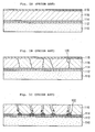
- Figs. 1A to 1C are cross-sectional views of a structure for showing a grain growth process in a copper metal layer, and an oxidation process in a barrier metal.
- a barrier metal composed of tantalum nitride (TaN) film 112 and tantalum (Ta) film 114 is formed on interlayer insulating film 110 deposited on a semiconductor substrate, not shown. Subsequently, a seed layer and copper metal layer 116 are formed on the barrier metal. As copper metal layer 116 is exposed to the atmosphere after the formation, the surface of copper metal layer 116 is oxidized to form copper oxide 118 on the surface of copper metal layer 116, as illustrated in Fig.1A.
- the tantalum oxide compound may give rise to the following problems.
- Copper oxide 118 remaining on copper metal layer 116 is removed in the subsequent CMP processing.
- the tantalum oxide compound formed on the interface between the barrier metal and copper metal layer 116 still remains within the subsequently formed wires.
- the residual tantalum oxide compound degrades the adhesivity of copper metal layer 116 to the barrier metal, resulting in a lower reliability of wires, particularly, deteriorated stress-migration and electro-migration.
- the residual tantalum oxide compound can also cause a stress-induced-voiding in which stresses produce voids in the wires.
- the laminate metal film is once immersed in a solution including an organic acid having at least one carboxyl group before a heat treatment, thereby removing from the laminate metal film an oxide which is the source of oxygen that diffuses during the heat treatment. It is therefore possible to prevent the barrier metal from reacting with oxygen and therefore suppress the generation of an oxide on the interface between the barrier metal and copper metal layer. Consequently, the method of the present invention can prevent degraded adhesivity of the copper metal layer to the barrier metal, and prevent deteriorated stress-migration and electro-migration for a wire using the laminate metal film. The method of the present invention can further prevent a stress-induced-voiding in the wire using the laminate metal film.
- oxide film (SiO 2 film) 12 is formed on the semiconductor elements in a thickness of 100 - 300 nm as an interlayer insulating film.
- SiCN film 14 is formed on SiO 2 film 12 in a thickness of 10 - 150 nm as an etching stopper film for improving wire workability.
- SiO 2 film 16 is formed on SiCN film 14 in a thickness of 100 - 1800 nm as an insulating film for the formation of wires.
- the SiCN film which serves as an etching stopper film is called the "stopper SiCN film.” Also, in a process of sequentially forming semiconductor elements such as transistors, resistors, capacitors, and the like as well as wires for connecting the semiconductor elements on the semiconductor substrate, the semiconductor substrate including such semiconductor elements formed thereon is collectively called the "wafer.”
- SiO 2 film 16 is etched until stopper SiCN film 14 is exposed. After removing the resist pattern, Stopper SiCN film 14 is etched away using SiO 2 film 16 as a mask to form groove 18 for wiring (Fig. 2B).
- a TaN film 1 - 40 nm thick and Ta film 1 - 40 nm thick are deposited in order by sputtering to form barrier metal 20 composed of the TaN film and Ta film.
- a seed layer mainly containing copper is formed on barrier metal 20.
- the wafer is immersed in an electrolyte plating solution containing copper sulfate (CuSO 4 ) to form copper metal layer 22 on the seed layer in a thickness of 40 - 3000 nm by an electrolyte plating method, thereby forming laminate metal film 24 composed of barrier metal 20 and copper metal layer 22 (Fig. 2C).
- CuSO 4 copper sulfate
- the organic acid solution used herein is an oxalic acid solution which includes oxalic acid ((COOH) 2 ) in volume concentration of 0.1 - 3 % as an organic acid which includes at least one carboxyl group.
- This organic acid solution treatment removes the copper oxide. After the organic acid solution treatment, moisture is removed by a spin dry method to dry the wafer.
- the wafers are annealed for growing copper grains (copper grain growth annealing) at temperatures of 200 - 450 °C, in an inert gas atmosphere mainly provided by an N 2 gas for a processing time of 10 - 200 minutes.
- laminate metal film 24 is polished by CMP processing until the top surface of SiO 2 film 16 is exposed, followed by formation of copper wire 26 composed of barrier metal 20 and copper metal layer 22.
- copper wire 26 composed of barrier metal 20 and copper metal layer 22.
- the CMP processing as abrasive particles sticking on the top surface of the copper wire is washed away, water reacts with copper during the washing to form a copper oxide layer on the top surface of the copper wire.
- the copper oxide layer is exposed to a 1 % diluted solution of benzotriazole (BTA) to make BTA react with the copper oxide layer to form a BTA layer which serves as an oxidization preventing layer.
- BTA benzotriazole
- cap SiCN film 28 is formed in a thickness of 10 - 150 nm as a copper diffusion preventing film by a CVD method (Fig. 2D).
- pads for electrically connecting a circuit comprising semiconductor elements, copper wires, and the like to the outside, and a passivation film are formed.
- Two sample wafers used in the evaluation were fabricated in the following manner. Two wafers, which have been processed up to the step illustrated in Fig. 2C, were prepared. Before the copper grain growth annealing, one of the two wafers underwent the organic acid solution treatment, whereas the other wafer did not undergo the organic acid solution treatment. Then, the two wafers underwent the copper grain growth annealing, CMP processing, and washing.
- locations of wire defects were counted on each of the wafers for comparison.
- the wire defect location was identified by comparing a wiring pattern formed on each of the wafers with a wiring pattern of a reference exposure mask to find a location on the wafer under evaluation at which the pattern was different from that at a corresponding location on the reference exposure mask, determining that the pattern was missing at this location, and regarding this location as the location of a defect.
- a wafer is formed on its surface with a plurality of shots, each of which is a wiring pattern on an exposure mask transferred onto the wafer. Thus, locations of wire defects were identified for all shots within the surface of each wafer.
- Figs. 3A and 3B are defect distribution diagrams each showing the locations of defects on the surface of a wafer.
- Fig. 3A is a defect distribution diagram for the wafer which had not been treated with the organic acid solution before the copper grain growth annealing.
- Fig. 3B is a defect distributing diagram for the wafer which had been treated with the organic acid solution before the copper grain growth annealing.
- wire defects were found at 57 locations over the entire surface of the wafer which had not been treated with the organic acid.
- component elements at the locations of the wire defects were analyzed after removing copper metal layer 22, and Ta and oxygen were detected. It was found from this analysis that a tantalum oxide compound was formed at those locations.
- wire defects were found at 19 locations on the surface of the wafer which had been treated with the organic acid. It was readily confirmed from the result of the analysis that the defects at these 19 locations were caused only by scratches in the CMP processing and losses of the pattern in micro-machining.
- the aforementioned oxalic acid solution contained the oxalic acid in a concentration of 0.1 - 3 %, the concentration of the oxalic acid is not limited in this range.
- the organic acid for removing the copper oxide is not limited to oxalic acid, but may be any compound which belongs to any of monocarboxylic acid, dicarboxylic acid, tricarboxylic acid, oxycarboxylic acid, and aminocarboxylic acid.
- a wafer formed with a laminate metal film having a copper metal layer and a barrier metal is immersed in a solution including an organic acid having at least one carboxyl group, before the copper grain growth annealing, to remove from the laminate metal film such an oxide which can be the source of oxygen that diffuses during the annealing. It is therefore possible to eliminate the oxide produced by the reaction of the barrier metal with oxygen during the copper grain growth annealing.
- the organic acid solution treatment removes from the copper metal layer those residual plating components other than oxygen, such as sulfur contained in an electrolyte plating solution, the resulting wafer is prevented from a degraded reliability due to the residual plating components such as sulfur, particularly, deteriorated stress-migration and electro-migration. Furthermore, the wafer is also prevented from the stress-induced-voiding.
- the wafer is chemically and mechanically polished after the copper grain growth annealing
- the CMP processing may be followed by the copper grain growth annealing, in which case the wafer may be treated with an organic acid solution, as mentioned above, before the copper grain growth annealing to remove a copper oxide formed on the surfaces of the copper metal layer and barrier metal, so that similar advantages can be provided.
- copper wires may be formed in a plurality of layers.
- via plugs may be provided for electrically connecting the copper wires formed in the different layers.
- the via plugs also have a barrier metal and a copper metal layer in a manner similar to the copper wires, the aforementioned advantages can be provided for the via plugs as well by the organic acid solution treatment before the copper grain growth annealing.
- the copper grain growth annealing is not limited to the implementation in the batch furnace annealing apparatus, but may be implemented in a single wafer RTP (Rapid Thermal Process) apparatus which processes wafers one by one.
- RTP Rapid Thermal Process
- hydrogen (H 2 ) may be included in the annealing atmosphere. This is because hydrogen atoms are trapped by unbonded hands on the copper grain boundaries to facilitate the flow of a current among copper grains.
- the etching stopper film may be made of any of an SiON film, an SiN film, an SiO 2 film, and a SiC film, or a laminate film of these films, other than the SiCN film.
- the interlayer insulating film, and the insulating film for forming a wire may be made of any of an organic film, an HSQ (hydrogensilsesquioxane)-based film, an MSQ (methylsilsesquioxane)-based film, and L-Ox (a registered trade name of NEC Electronics Corporation) film which is a film having a ladder-type hydrogenated siloxane structure, or a laminate film of these films, other than the SiO 2 film.
- HSQ hydrogensilsesquioxane
- MSQ methylsilsesquioxane
- L-Ox a registered trade name of NEC Electronics Corporation
- the copper metal layer may contain a trace of other elements such as Si, Al and the like.
Landscapes
- Internal Circuitry In Semiconductor Integrated Circuit Devices (AREA)
- Electrodes Of Semiconductors (AREA)
Abstract
Description
Claims (12)
- A method of manufacturing a semiconductor device which is formed with a laminate metal film having a copper metal layer mainly containing copper and a barrier layer containing a metal more susceptible to oxidization than copper, said method comprising the steps of:forming a barrier layer on the bottom and sides of a recess formed in an insulating film on a semiconductor substrate;forming said copper metal layer such that said copper metal layer covers said barrier layer and fills in said recess;removing an oxide formed on the surface of said copper metal layer due to exposure of the surface of said copper metal layer to oxygen with a solution including an organic acid having at least one carboxyl group; andperforming a heat treatment for growing grains of the copper.
- The method of manufacturing a semiconductor device according to claim 1, wherein said organic acid is a compound which belongs to any of monocarboxylic acid, dicarboxylic acid, tricarboxylic acid, oxycarboxylic acid, and aminocarboxylic acid.
- The method of manufacturing a semiconductor device according to claim 2, wherein said compound is oxalic acid.
- The method of manufacturing a semiconductor device according to claim 1, wherein said heat treatment is performed in an inert atmosphere.
- The method of manufacturing a semiconductor device according to claim 1, wherein said barrier layer is a metal layer including tantalum.
- The method of manufacturing a semiconductor device according to claim 1, wherein said laminate metal film is used as a wire or a via plug for connecting wires to each other.
- A method of manufacturing a semiconductor device which is formed with a laminate metal film having a copper metal layer mainly containing copper and a barrier layer containing a metal more susceptible to oxidization than copper, said method comprising the steps of:forming a barrier layer on the bottom and sides of a recess formed in an insulating film on a semiconductor substrate;forming said copper metal layer such that said copper metal layer covers said barrier layer and fills in said recess;polishing said laminate metal film until the top surface of said insulating film is exposed;removing an oxide formed on the surface of said copper metal layer due to exposure of the surface of said copper metal layer to oxygen with a solution including an organic acid having at least one carboxyl group; andperforming a heat treatment for growing grains of the copper.
- The method of manufacturing a semiconductor device according to claim 7, wherein said organic acid is a compound which belongs to any of monocarboxylic acid, dicarboxylic acid, tricarboxylic acid, oxycarboxylic acid, and aminocarboxylic acid.
- The method of manufacturing a semiconductor device according to claim 8, wherein said compound is oxalic acid.
- The method of manufacturing a semiconductor device according to claim 7, wherein said heat treatment is performed in an inert atmosphere.
- The method of manufacturing a semiconductor device according to claim 7, wherein said barrier layer is a metal layer including tantalum.
- The method of manufacturing a semiconductor device according to claim 7, wherein said laminate metal film is used as a wire or a via plug for connecting wires to each other.
Applications Claiming Priority (2)
| Application Number | Priority Date | Filing Date | Title |
|---|---|---|---|
| JP2003021956 | 2003-01-30 | ||
| JP2003021956A JP4209212B2 (en) | 2003-01-30 | 2003-01-30 | Manufacturing method of semiconductor device |
Publications (2)
| Publication Number | Publication Date |
|---|---|
| EP1443551A2 true EP1443551A2 (en) | 2004-08-04 |
| EP1443551A3 EP1443551A3 (en) | 2005-01-12 |
Family
ID=32652890
Family Applications (1)
| Application Number | Title | Priority Date | Filing Date |
|---|---|---|---|
| EP04001235A Withdrawn EP1443551A3 (en) | 2003-01-30 | 2004-01-21 | Semiconductor device manufacturing method for improving adhesiveness of copper metal layer to barrier layer |
Country Status (4)
| Country | Link |
|---|---|
| US (1) | US6821882B2 (en) |
| EP (1) | EP1443551A3 (en) |
| JP (1) | JP4209212B2 (en) |
| CN (1) | CN1295761C (en) |
Families Citing this family (10)
| Publication number | Priority date | Publication date | Assignee | Title |
|---|---|---|---|---|
| US7867906B2 (en) * | 2005-06-22 | 2011-01-11 | Nec Corporation | Semiconductor device and method for manufacturing same |
| KR101020452B1 (en) * | 2006-03-27 | 2011-03-08 | 도쿄엘렉트론가부시키가이샤 | Substrate processing method, semiconductor device manufacturing method, substrate processing apparatus, and recording medium |
| CN1917285A (en) * | 2006-09-06 | 2007-02-21 | 上海集成电路研发中心有限公司 | Antenna structure on IC and manufacturing method |
| TWI383450B (en) * | 2007-03-13 | 2013-01-21 | Fujitsu Ltd | Semiconductor device and manufacturing method therefor |
| CN101627463B (en) * | 2007-03-13 | 2012-05-30 | 富士通株式会社 | Semiconductor device and process for producing the same |
| JP6011074B2 (en) * | 2012-01-20 | 2016-10-19 | 富士通株式会社 | Electronic device manufacturing method and electronic device manufacturing apparatus |
| CN104241191B (en) * | 2013-06-07 | 2017-06-06 | 上海华虹宏力半导体制造有限公司 | A kind of metal wire film forming process |
| CN103441129A (en) | 2013-08-23 | 2013-12-11 | 京东方科技集团股份有限公司 | Array substrate, manufacturing method of array substrate and display device |
| CN104637862B (en) * | 2013-11-14 | 2019-10-18 | 盛美半导体设备(上海)有限公司 | Semiconductor Structure Formation Method |
| US11192822B2 (en) * | 2018-11-08 | 2021-12-07 | Western Digital Technologies, Inc. | Enhanced nickel plating process |
Family Cites Families (12)
| Publication number | Priority date | Publication date | Assignee | Title |
|---|---|---|---|---|
| JP3277098B2 (en) * | 1994-07-26 | 2002-04-22 | 株式会社東芝 | Method for manufacturing semiconductor device |
| JP3500564B2 (en) * | 1997-12-19 | 2004-02-23 | 富士通株式会社 | Method for manufacturing semiconductor device |
| JPH11269693A (en) | 1998-03-24 | 1999-10-05 | Japan Energy Corp | Copper deposition method and copper plating solution |
| JPH11312680A (en) * | 1998-04-30 | 1999-11-09 | Nec Corp | Wiring formation method |
| JP3348785B2 (en) | 1999-11-25 | 2002-11-20 | 日本電気株式会社 | Semiconductor device and manufacturing method thereof |
| JP2001298028A (en) | 2000-04-17 | 2001-10-26 | Tokyo Electron Ltd | Semiconductor device manufacturing method |
| JP2002110679A (en) * | 2000-09-29 | 2002-04-12 | Hitachi Ltd | Method for manufacturing semiconductor integrated circuit device |
| US6790763B2 (en) * | 2000-12-04 | 2004-09-14 | Ebara Corporation | Substrate processing method |
| JP4535629B2 (en) * | 2001-02-21 | 2010-09-01 | ルネサスエレクトロニクス株式会社 | Manufacturing method of semiconductor device |
| US6692546B2 (en) * | 2001-08-14 | 2004-02-17 | Advanced Technology Materials, Inc. | Chemical mechanical polishing compositions for metal and associated materials and method of using same |
| US6800218B2 (en) * | 2001-08-23 | 2004-10-05 | Advanced Technology Materials, Inc. | Abrasive free formulations for chemical mechanical polishing of copper and associated materials and method of using same |
| JP2003142579A (en) * | 2001-11-07 | 2003-05-16 | Hitachi Ltd | Semiconductor device manufacturing method and semiconductor device |
-
2003
- 2003-01-30 JP JP2003021956A patent/JP4209212B2/en not_active Expired - Fee Related
-
2004
- 2004-01-16 US US10/758,392 patent/US6821882B2/en not_active Expired - Fee Related
- 2004-01-21 EP EP04001235A patent/EP1443551A3/en not_active Withdrawn
- 2004-01-29 CN CNB2004100035454A patent/CN1295761C/en not_active Expired - Fee Related
Also Published As
| Publication number | Publication date |
|---|---|
| CN1295761C (en) | 2007-01-17 |
| US20040152306A1 (en) | 2004-08-05 |
| CN1519897A (en) | 2004-08-11 |
| US6821882B2 (en) | 2004-11-23 |
| JP4209212B2 (en) | 2009-01-14 |
| EP1443551A3 (en) | 2005-01-12 |
| JP2004235415A (en) | 2004-08-19 |
Similar Documents
| Publication | Publication Date | Title |
|---|---|---|
| KR100746543B1 (en) | Manufacturing method of semiconductor integrated circuit device | |
| US7259091B2 (en) | Technique for forming a passivation layer prior to depositing a barrier layer in a copper metallization layer | |
| TW483105B (en) | A semiconductor integrated circuit device and a method of manufacturing the same | |
| JP4647184B2 (en) | Manufacturing method of semiconductor device | |
| US20070145591A1 (en) | Semiconductor device and manufacturing method therof | |
| JP2003332426A (en) | Semiconductor device manufacturing method and semiconductor device | |
| JP2003188254A (en) | Semiconductor device manufacturing method and semiconductor device | |
| JPWO2004061931A1 (en) | Semiconductor device having multilayer wiring structure and method for manufacturing the same | |
| US6821882B2 (en) | Semiconductor device manufacturing method for improving adhesivity of copper metal layer to barrier layer | |
| JP4034227B2 (en) | Manufacturing method of semiconductor device | |
| US7232763B2 (en) | Method of manufacturing semiconductor device | |
| US6348410B1 (en) | Low temperature hillock suppression method in integrated circuit interconnects | |
| US6465867B1 (en) | Amorphous and gradated barrier layer for integrated circuit interconnects | |
| JP5117755B2 (en) | Semiconductor device | |
| US6482755B1 (en) | HDP deposition hillock suppression method in integrated circuits | |
| US20100190335A1 (en) | Method of manufacturing semiconductor device | |
| US8390135B2 (en) | Semiconductor device | |
| US7253097B2 (en) | Integrated circuit system using dual damascene process | |
| US6841473B1 (en) | Manufacturing an integrated circuit with low solubility metal-conductor interconnect cap | |
| US8329584B2 (en) | Method of manufacturing semiconductor device | |
| KR100746895B1 (en) | Manufacturing Method of Semiconductor Integrated Circuit Device | |
| JP2006179948A (en) | Semiconductor device and method of manufacturing device | |
| JP2006216809A (en) | Semiconductor device and manufacturing method thereof | |
| CN102760685A (en) | Etching post-processing method of copper interconnection line | |
| US6455422B1 (en) | Densification process hillock suppression method in integrated circuits |
Legal Events
| Date | Code | Title | Description |
|---|---|---|---|
| PUAI | Public reference made under article 153(3) epc to a published international application that has entered the european phase |
Free format text: ORIGINAL CODE: 0009012 |
|
| AK | Designated contracting states |
Kind code of ref document: A2 Designated state(s): AT BE BG CH CY CZ DE DK EE ES FI FR GB GR HU IE IT LI LU MC NL PT RO SE SI SK TR |
|
| AX | Request for extension of the european patent |
Extension state: AL LT LV MK |
|
| PUAL | Search report despatched |
Free format text: ORIGINAL CODE: 0009013 |
|
| AK | Designated contracting states |
Kind code of ref document: A3 Designated state(s): AT BE BG CH CY CZ DE DK EE ES FI FR GB GR HU IE IT LI LU MC NL PT RO SE SI SK TR |
|
| AX | Request for extension of the european patent |
Extension state: AL LT LV MK |
|
| 17P | Request for examination filed |
Effective date: 20041202 |
|
| AKX | Designation fees paid |
Designated state(s): DE FR |
|
| STAA | Information on the status of an ep patent application or granted ep patent |
Free format text: STATUS: THE APPLICATION HAS BEEN WITHDRAWN |
|
| 18W | Application withdrawn |
Effective date: 20100304 |