EP1443520A2 - Semiconductor memory device - Google Patents
Semiconductor memory device Download PDFInfo
- Publication number
- EP1443520A2 EP1443520A2 EP04250463A EP04250463A EP1443520A2 EP 1443520 A2 EP1443520 A2 EP 1443520A2 EP 04250463 A EP04250463 A EP 04250463A EP 04250463 A EP04250463 A EP 04250463A EP 1443520 A2 EP1443520 A2 EP 1443520A2
- Authority
- EP
- European Patent Office
- Prior art keywords
- virtual ground
- line
- memory cell
- memory cells
- lines
- Prior art date
- Legal status (The legal status is an assumption and is not a legal conclusion. Google has not performed a legal analysis and makes no representation as to the accuracy of the status listed.)
- Withdrawn
Links
Images






Classifications
-
- G—PHYSICS
- G11—INFORMATION STORAGE
- G11C—STATIC STORES
- G11C17/00—Read-only memories programmable only once; Semi-permanent stores, e.g. manually-replaceable information cards
- G11C17/08—Read-only memories programmable only once; Semi-permanent stores, e.g. manually-replaceable information cards using semiconductor devices, e.g. bipolar elements
- G11C17/10—Read-only memories programmable only once; Semi-permanent stores, e.g. manually-replaceable information cards using semiconductor devices, e.g. bipolar elements in which contents are determined during manufacturing by a predetermined arrangement of coupling elements, e.g. mask-programmable ROM
- G11C17/12—Read-only memories programmable only once; Semi-permanent stores, e.g. manually-replaceable information cards using semiconductor devices, e.g. bipolar elements in which contents are determined during manufacturing by a predetermined arrangement of coupling elements, e.g. mask-programmable ROM using field-effect devices
- G11C17/126—Virtual ground arrays
-
- G—PHYSICS
- G09—EDUCATION; CRYPTOGRAPHY; DISPLAY; ADVERTISING; SEALS
- G09B—EDUCATIONAL OR DEMONSTRATION APPLIANCES; APPLIANCES FOR TEACHING, OR COMMUNICATING WITH, THE BLIND, DEAF OR MUTE; MODELS; PLANETARIA; GLOBES; MAPS; DIAGRAMS
- G09B5/00—Electrically-operated educational appliances
- G09B5/08—Electrically-operated educational appliances providing for individual presentation of information to a plurality of student stations
- G09B5/14—Electrically-operated educational appliances providing for individual presentation of information to a plurality of student stations with provision for individual teacher-student communication
-
- G—PHYSICS
- G06—COMPUTING OR CALCULATING; COUNTING
- G06Q—INFORMATION AND COMMUNICATION TECHNOLOGY [ICT] SPECIALLY ADAPTED FOR ADMINISTRATIVE, COMMERCIAL, FINANCIAL, MANAGERIAL OR SUPERVISORY PURPOSES; SYSTEMS OR METHODS SPECIALLY ADAPTED FOR ADMINISTRATIVE, COMMERCIAL, FINANCIAL, MANAGERIAL OR SUPERVISORY PURPOSES, NOT OTHERWISE PROVIDED FOR
- G06Q50/00—Information and communication technology [ICT] specially adapted for implementation of business processes of specific business sectors, e.g. utilities or tourism
- G06Q50/10—Services
- G06Q50/20—Education
- G06Q50/205—Education administration or guidance
-
- G—PHYSICS
- G09—EDUCATION; CRYPTOGRAPHY; DISPLAY; ADVERTISING; SEALS
- G09B—EDUCATIONAL OR DEMONSTRATION APPLIANCES; APPLIANCES FOR TEACHING, OR COMMUNICATING WITH, THE BLIND, DEAF OR MUTE; MODELS; PLANETARIA; GLOBES; MAPS; DIAGRAMS
- G09B5/00—Electrically-operated educational appliances
- G09B5/06—Electrically-operated educational appliances with both visual and audible presentation of the material to be studied
-
- G—PHYSICS
- G11—INFORMATION STORAGE
- G11C—STATIC STORES
- G11C11/00—Digital stores characterised by the use of particular electric or magnetic storage elements; Storage elements therefor
- G11C11/56—Digital stores characterised by the use of particular electric or magnetic storage elements; Storage elements therefor using storage elements with more than two stable states represented by steps, e.g. of voltage, current, phase, frequency
- G11C11/5685—Digital stores characterised by the use of particular electric or magnetic storage elements; Storage elements therefor using storage elements with more than two stable states represented by steps, e.g. of voltage, current, phase, frequency using storage elements comprising metal oxide memory material, e.g. perovskites
-
- G—PHYSICS
- G11—INFORMATION STORAGE
- G11C—STATIC STORES
- G11C13/00—Digital stores characterised by the use of storage elements not covered by groups G11C11/00, G11C23/00, or G11C25/00
- G11C13/0002—Digital stores characterised by the use of storage elements not covered by groups G11C11/00, G11C23/00, or G11C25/00 using resistive RAM [RRAM] elements
- G11C13/0007—Digital stores characterised by the use of storage elements not covered by groups G11C11/00, G11C23/00, or G11C25/00 using resistive RAM [RRAM] elements comprising metal oxide memory material, e.g. perovskites
-
- G—PHYSICS
- G11—INFORMATION STORAGE
- G11C—STATIC STORES
- G11C13/00—Digital stores characterised by the use of storage elements not covered by groups G11C11/00, G11C23/00, or G11C25/00
- G11C13/0002—Digital stores characterised by the use of storage elements not covered by groups G11C11/00, G11C23/00, or G11C25/00 using resistive RAM [RRAM] elements
- G11C13/0021—Auxiliary circuits
- G11C13/0023—Address circuits or decoders
-
- G—PHYSICS
- G11—INFORMATION STORAGE
- G11C—STATIC STORES
- G11C13/00—Digital stores characterised by the use of storage elements not covered by groups G11C11/00, G11C23/00, or G11C25/00
- G11C13/0002—Digital stores characterised by the use of storage elements not covered by groups G11C11/00, G11C23/00, or G11C25/00 using resistive RAM [RRAM] elements
- G11C13/0021—Auxiliary circuits
- G11C13/0023—Address circuits or decoders
- G11C13/0026—Bit-line or column circuits
-
- G—PHYSICS
- G11—INFORMATION STORAGE
- G11C—STATIC STORES
- G11C13/00—Digital stores characterised by the use of storage elements not covered by groups G11C11/00, G11C23/00, or G11C25/00
- G11C13/0002—Digital stores characterised by the use of storage elements not covered by groups G11C11/00, G11C23/00, or G11C25/00 using resistive RAM [RRAM] elements
- G11C13/0021—Auxiliary circuits
- G11C13/004—Reading or sensing circuits or methods
-
- G—PHYSICS
- G11—INFORMATION STORAGE
- G11C—STATIC STORES
- G11C13/00—Digital stores characterised by the use of storage elements not covered by groups G11C11/00, G11C23/00, or G11C25/00
- G11C13/0002—Digital stores characterised by the use of storage elements not covered by groups G11C11/00, G11C23/00, or G11C25/00 using resistive RAM [RRAM] elements
- G11C13/0021—Auxiliary circuits
- G11C13/0064—Verifying circuits or methods
-
- G—PHYSICS
- G11—INFORMATION STORAGE
- G11C—STATIC STORES
- G11C16/00—Erasable programmable read-only memories
- G11C16/02—Erasable programmable read-only memories electrically programmable
- G11C16/04—Erasable programmable read-only memories electrically programmable using variable threshold transistors, e.g. FAMOS
- G11C16/0491—Virtual ground arrays
-
- G—PHYSICS
- G11—INFORMATION STORAGE
- G11C—STATIC STORES
- G11C16/00—Erasable programmable read-only memories
- G11C16/02—Erasable programmable read-only memories electrically programmable
- G11C16/06—Auxiliary circuits, e.g. for writing into memory
- G11C16/26—Sensing or reading circuits; Data output circuits
-
- G—PHYSICS
- G11—INFORMATION STORAGE
- G11C—STATIC STORES
- G11C16/00—Erasable programmable read-only memories
- G11C16/02—Erasable programmable read-only memories electrically programmable
- G11C16/04—Erasable programmable read-only memories electrically programmable using variable threshold transistors, e.g. FAMOS
- G11C16/0466—Erasable programmable read-only memories electrically programmable using variable threshold transistors, e.g. FAMOS comprising cells with charge storage in an insulating layer, e.g. metal-nitride-oxide-silicon [MNOS], silicon-oxide-nitride-oxide-silicon [SONOS]
- G11C16/0475—Erasable programmable read-only memories electrically programmable using variable threshold transistors, e.g. FAMOS comprising cells with charge storage in an insulating layer, e.g. metal-nitride-oxide-silicon [MNOS], silicon-oxide-nitride-oxide-silicon [SONOS] comprising two or more independent storage sites which store independent data
-
- G—PHYSICS
- G11—INFORMATION STORAGE
- G11C—STATIC STORES
- G11C2213/00—Indexing scheme relating to G11C13/00 for features not covered by this group
- G11C2213/30—Resistive cell, memory material aspects
- G11C2213/31—Material having complex metal oxide, e.g. perovskite structure
Definitions
- the present invention relates to a semiconductor memory device, particularly to a semiconductor memory device for reading stored data by selecting a word line, bit line, and virtual ground line to be connected to memory cells from which data will be read and selecting the memory cells.
- a nonvolatile semiconductor memory device such as a mask ROM (mask programmable Read Only Memory) or a flash memory by using the bit line and a virtual ground line.
- a nonvolatile semiconductor memory device such as a mask ROM (mask programmable Read Only Memory) or a flash memory by using the bit line and a virtual ground line.
- the method is described below by using a memory cell of a mask ROM having a simple memory cell structure.
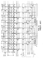
- Fig. 8 shows a conceptual view of a reading system using the virtual ground line.
- a bit line and a virtual ground line are alternately arranged along a column direction and word lines are arranged along a row direction on a memory cell array in which memory cells are arranged in the row direction and the column direction like a matrix
- a memory cell transistor constituted by a MOSFET is set between a bit line and a virtual ground line adjacent to each other, and the drain and source electrodes of a memory cell transistor are connected to the bit line and the virtual ground line respectively.
- the gate electrode of the memory cell transistor is connected to a word line.
- a plurality of memory cell transistors is connected to one word line to improve the area efficiency of the memory cell.
- a threshold value is set when each of the transistors is fabricated (binary data is programmed for each memory cell) so as to serve as either of a transistor having a high threshold (off transistor having a threshold higher than a high-level potential of a word line serving as a gate electrode and to be normally turned off independently of the word-line potential) and a transistor having a low threshold (on transistor to be turned on when a word line potential is higher than the threshold).
- a word line, bit line, and virtual ground line to be connected to a transistor from which data will be read are selected, the selected bit line is charged to a predetermined potential, the selected virtual ground line is grounded to the ground potential, and the selected word line is set to the high level.
- the difference of currents of an on-transistor and off-transistor under the above state is sensed by a sensing circuit to determine the binary data stored in the memory cell.
- a hierarchical bit line system for a large-capacity semiconductor memory device as a system for reading data from these memory cell arrays at a high speed.
- a memory cell array according to the hierarchical bit line system is constituted by dividing a memory cell array into a plurality of blocks, using the bit line of each block as an auxiliary bit line (also referred to as local bit line), and connecting every a plurality of auxiliary bit lines of each block to a main bit line (also referred to as global bit line) through a block selection transistor.
- a bit line for selecting a memory cell is selected by selecting a main bit line and selecting an auxiliary bit line to be connected to the selected main bit line by the block selection transistor.
- Fig. 9 shows a configuration of a memory array cell according to the hierarchical bit line system.
- a virtual ground line also uses the same hierarchical structure as that of a bit line.
- the block selection transistor BK1-1 or the like is selected by a bank selection line BLK1 or the like.
- a main bit line MB2 or the like is connected to an auxiliary bit line SB4 or the like through the block selection transistor BK1-1.
- the charging/grounding selection circuit 21, charging circuit 22, and sensing circuit 23 may be connected to a plurality of block selection circuits 20.
- the reading operation of the memory cell array circuit shown in Fig. 9 is described below.
- a case of selecting a memory cell transistor M4 and reading data from the M4 is assumed.
- the word line WLO to be connected to the gate of the transistor M4 is set to the high level and other word lines (WLn) are set to the low level.
- the control signal BLK1 of a block selection transistor is set to the high level in order to turn on the block selection transistor BK1-1
- the control signal BLK3 is set to the high level in order to turn on a block selection transistor BK3-2
- other control signals BLK2 and BLK4 are to the low level.
- a current route (MB2)-(BK1-1)-(SB4) extending from a main bit line to a memory cell and a current route (SB5)-(BK3-2)-(MB3) extending from the memory cell to a main virtual ground line are formed on the transistor M4.
- the transistor M4 When the transistor M4 is an on-transistor, by setting BSEL2 to the high level, VGSEL1 to the high level, BLOCKSEL1 to the high level, BSEL1 to the low level, and VGSEL2 to the lower level, the selected main bit line MB2 has a charging potential, the selected main virtual ground line MB3 has a ground potential, and current circulates through a route of (MB2)-(BK1-1)-(SB4)-(M4)-(SB5)-(BK3-2)-(MB3).
- the memory cell transistor M4 is an on-transistor.
- transistors M3, M2, M1, and M0 or the like of an unselected memory cell in the same row as the transistor M4 are on-transistors, a current route via the transistors M3, M2, and M1 is formed even if, for example, the transistor M4 is an off-transistor because the word line WLO serving as a gate line of each transistor is common. That is, when setting the selected main bit line MB2 to a charging potential, a transient current for charging the parasitic capacitance of a bit line or a virtual ground line connected to each memory cell circulates through a route of (MB2)-(BK1-1)-(SB4)-(M3)-(M2)-(M1)....
- the current circulating through the current route is temporarily referred to as an alternate discharge current.
- a current route extended from a selected main bit line to each bit line or virtual ground line is formed as if the transistor M4 from which data will be read is an on-transistor though it is an off-transistor and the operation margin of an erroneous reading operation or reading operation is decreased.
- a method of charging an unselected bit line and an unselected virtual ground line to a predetermined charging potential is conventionally used.
- an unselected main bit line MB0 and unselected main virtual ground line MB1 are set to a charging potential.
- An auxiliary bit line SB0 and an auxiliary virtual ground line SB1 are set to a charging potential through a block selection transistor.
- Japanese Unexamined Patent Publication No. 10-11991 discloses an improved connection system for a memory cell transistor and a block selection transistor.
- the unselected main bit line MB0 and unselected main virtual ground line MB1 respectively have a charging potential because a selected main bit line becomes MB2 and a selected virtual ground line becomes MB3 to charge an unselected bit line and unselected virtual ground line when reading data from the memory cell transistor M4 similarly to the above description, the unselected main bit line MB4 and unselected main virtual ground line MB5 are further charged at the same time.
- the unselected main bit line MB4 and unselected main virtual ground line MB5 extend through their respective block selection transistors, an auxiliary bit line SB8 and auxiliary virtual ground line SB9 respectively have a charging potential, and a current route extending to (SB8)-(M7)-(M6)-(M5)-(SB5) to charge the selected auxiliary virtual ground line SB5 is formed.
- the current circulating through the current route is temporarily referred to as alternate injection current.
- the alternate injection current raises the ground potential of the auxiliary virtual ground line SB5 and decreases the reading current of the selected main bit line MB2 circulating through (MB2)-(BK1-1)-(SB4)-(M4)-(SB5)-(BK3-2)-(MB3).
- the decrease of the reading current not only decreases the reading speed of a memory cell but also decreases a reading operation margin because a selected memory cell transistor may be erroneously read.
- the current corresponding to the alternate injection current is basically present. That is, when all the unselected memory cell transistors present between the transistors M12 and M4 are on-transistors, charging unselected bit lines and unselected virtual ground lines necessary for the data reading when the transistor M12 is an off-transistor decreases the reading current when the transistor M4 is an on-transistor by the current corresponding to the alternate injection current. However, the reading current when the transistor M4 is an on-transistor is still decreased.
- the operation margin decrease measure disclosed in Japanese Unexamined Patent Publication No. 10-11991 also decreases the alternate injection current flowing into the selected bit line. Moreover, to restrict the control of these bit line and virtual ground line, the number of cells to be simultaneously read by the same word line is restricted and this greatly prevents the capacity of a memory cell array from increasing.
- a semiconductor memory device of the present invention comprises a memory cell array constituted by arranging memory cells respectively having one first electrode and a pair of second electrodes and capable of reading stored contents in accordance with a state of the electrical connection between the second electrodes in the row and the column directions like a matrix correspondingly to the potential of the first electrode, connecting the first electrodes of the memory cells in the same row to a common word line, connecting a pair of the second electrodes each other between two of the memory cells adjacent to each other in the row direction, connecting one-hand second electrodes of the memory cells in the same column to a common bit line, and connecting the other-hand second electrodes of the memory cells to a common virtual ground line.
- the memory cell array is constituted by being divided into subarrays of at least a plurality of columns, and memory cell columns at the both ends of the subarrays are connected to an independent bit line or virtual ground line while the second electrodes are not connected but separated between two of the memory cells adjacent to each other in the row direction at the both sides of boundaries between the subarrays so that one of the word lines, one of the bit lines, and one of the virtual ground lines are selected and one memory cell from which data will be read is selected.
- a semiconductor memory device of the present invention for achieving the above object is constituted so that the bit line and the virtual ground line respectively have the function of the both and when one line performs the function of the other line, the other line performs the function of the one line instead of or in addition to the above characteristic configuration constituted so that one of the word lines, one of the bit lines, and one of the virtual ground lines are selected and one memory cell from which data will be read is selected.
- a memory cell from which data will be read purposed by the present invention is a memory cell having one first electrode and a pair of second electrodes and capable of reading stored contents in accordance with the state of electrical connection between the second electrodes correspondingly to the potential of the first electrode.
- directions of currents circulating through the second electrodes may be fixed or asymmetric depending on a programmed state.
- one of the second electrodes to be connected to a bit line and one of them to be connected to a virtual ground line may depend on a programmed state.
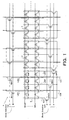
- FIG. 1 is an essential-portion circuit diagram showing a first embodiment of a memory cell array configuration 1 of the present invention device. Because this embodiment has a technical content relating to a data reading operation, a memory cell of a mask ROM constituted by one transistor and having a simple memory cell structure is described.
- a memory cell generally has one first electrode and a pair of second electrodes and a configuration capable of reading stored contents in accordance with the state of electrical connection between the second electrodes correspondingly to the potential of the first electrode.
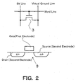
- the gate electrode of an n-channel MOSFET constituting a memory cell transistor 3 correspond to the first electrode and the drain and source electrodes of the MOSFET correspond to the second electrodes respectively.
- the state of electrical connection between the second electrodes is decided by the threshold voltage of the MOSFET and the threshold voltage is set in accordance with programmed data in the fabrication stage.
- the reading operation and data storing method of a single memory cell are the same as the contents described in the section of Description of the Related Art. Therefore, duplicate description is omitted and the same term is similarly used.
- a memory cell array 1 is constituted so that a plurality of memory cells is arranged like a matrix in the row direction (word-line extending direction) and the column direction (bit-line extending direction) and moreover, divided into a plurality of subarrays 2 in the row direction by a device isolation zone formed along the column direction every four cells.
- Each subarray 2 has a memory cell arrangement of (n+1) rows ⁇ 4 columns.
- the memory cells in the first column and fourth column are connected to an independent virtual ground line because a source electrode is isolated from the next subarray by a device isolation zone.
- This embodiment uses the hierarchical bit line system described in the section of Description of Related Art. When referring to a line merely as a bit line or virtual ground line in the following description, the line denotes an auxiliary bit line (local bit line) or an auxiliary virtual ground line (local virtual ground line).
- Each subarray 2 has one global bit line GB and one global virtual ground line GS, two bit lines LB 1 and LB2 are connected to the global bit line GB through first selection transistors BK1 and BK2, three virtual ground lines LS1, LS2, and LS3 are connected to the global virtual ground line GS through second selection transistors BK3, BK4, and BK5.
- the first selection transistors BK1 and BK2 are collectively arranged at one end of the subarray 2 in the column direction and the second selection transistors BK3, BK4, and BK5 are collectively arranged at the other end of the subarray 2 in the column direction, and word lines WL0 to WOn are arranged between block selection lines A and B for controlling gate electrodes of the first selection transistors BK1 and BK2 respectively and block selection lines C, D, and E for controlling gate electrodes of the second selection transistors BK3, BK4, and BK5 respectively.
- the word line WLO is selectively set to the high level in order to select the memory cell M1 in the row direction. Then, to select the memory cell M1 on the column direction, the bit line LB 1 and virtual ground line LS 1 to be connected to the memory cell M1 are selected.
- the bit line LB1 and virtual ground line LS1 are selected by selecting the global bit line GB and a global virtual ground line GS as objects from which data will be read, setting the block selection lines B and C to the high level, turning on the first selection transistor BK1 and second selection transistor BK3, and connecting the bit line LB1 and virtual ground line LS1 to the global bit line GB and global virtual ground line GS through the first selection transistor BK1 and the second selection transistor BK3 respectively.
- the block selection line A is set to the high level and the first selection transistor BK2 is turned on in addition to the above state.
- the global bit line GB By charging the global bit line GB to a predetermined charging potential from a charging circuit (not shown) under the above state and setting the global virtual ground line GS to the ground potential, the bit lines LB1 and LB2 are charged and the virtual ground line LS1 becomes the ground potential.
- the gate electrode of the memory cell M1 from which data will be read is set to the high level and a charging potential is applied to the drain electrode of the memory cell M1 and the ground potential is applied to the source electrode of M1.
- the charging potential is simultaneously applied to the bit line LB2.
- the memory cell M1 is read by sensing a potential change of the global bit line GB following a potential change of the bit line LB1 by a sensing circuit (not shown). In this case, when the potential change amplitude of the bit line LB 1 decreases, a reading operation margin decreases and a reading speed lowers.
- the memory cell M1 is an on-transistor, that is, when the charging potential of the bit line LB1 lowers, the potential of the global bit line GB also lowers and moreover, the potential of the bit line LB2 lowers by following the above potentials through the first selection transistor BK2. Therefore, an alternate injection current is avoided from being generated and thus, a reading operation margin does not decrease.
- the word line WL0 is selectively set to the high level in order to select the memory cell M2 in the row direction. Then, the bit line LB 1 and virtual ground line LS2 to be connected to the memory cell M2 are selected in order to the memory cell M2 in the column direction.
- the bit line LB 1 and virtual ground line LS2 are selected by selecting the global bit line GB and global virtual ground line GS as objects from which data will be read, setting the block selection lines B and D to the high level, turning on the first selection transistor BK1 and second selection transistor BK4, and connecting the bit line LB1 and virtual ground line LS2 to the global bit line GB and global virtual ground line GS through the first selection transistor BK1 and second selection transistor BK4 respectively.
- the bit line LB 1 is charged and the virtual ground line LS2 becomes the ground potential.
- the gate electrode of the memory cell M2 from which data will be read is set to the high level, the charging potential is applied to the drain electrode of M2 and the ground potential is applied to the source electrode of M2.
- the reading operation of the memory cell M2 is the same as that of the memory cell M1.
- the alternate discharge current becomes a problem when the next memory cell M1 is an on-transistor.
- the alternate discharge current is not generated any more when charging the virtual ground line LS1 is completed through the memory cell M1 because the memory cell M1 is electrically completely isolated from the next subarray by a device isolation zone at the opposite side of the memory cell M2.
- the memory cell M2 is selected as an object from which data will be read, no alternate injection current is generated because the bit line LB2 to be connected only to an unselected memory cell is not charged. Therefore, also when the memory cell M2 is an object from which data will be read, a reading operation margin does not decrease.
- the memory cell M2 does not affect a reading operation. If the bit line LB2 and virtual ground line LS3 are charged for any reason, charged states of the bit line LB2 and virtual ground line LS3 may affect the case of setting the selected virtual ground line LS2 to the ground potential when the memory cells M3 and M4 are on-transistors. Therefore, the effect capable of preventing the above problem can be expected by turning on the second selection transistor BK5 and setting the virtual ground line LS3 to the ground potential.
- the word line WLO is selectively set to the high level in order to select the memory cell M3 in the row direction. Then, the bit line LB2 and virtual ground line LS2 to be connected to the memory cell M3 are selected in order to select the memory cell M3 in the column direction.
- the bit line LB2 and virtual ground line LS2 are selected by selecting the global bit line GB and global virtual ground line GS as objects from which data will be read, setting the block selection lines A and D to the high level, turning on the first selection transistor BK2 and second selection transistor BK4, and connecting the bit line LB2 and virtual ground line LS2 to the global bit line GB and global virtual ground line GS through the first selection transistor BK2 and second selection transistor BK4 respectively.
- reading data from the memory cell M3 is the same as the case of reading data from the memory cell M2 except only the fact that reading data from the memory cell M2 and a bit line to be selected are different. Therefore, descriptions of a reading operation and reading operation margin are omitted.
- the word line WL0 is set to the high level in order to select the memory cell M4 in the row direction. Then, the bit line LB2 and virtual ground line LS3 to be connected to the memory cell M4 are selected in order to select the memory cell 4 in the column direction.
- the bit line LB2 and virtual ground line LS3 are selected by selecting the global bit line GB and global virtual ground line GS as objects from which data will be read, setting the block selection lines A and E to the high level, turning on the first selection transistor BK2 and second selection transistor BK5, and connecting the bit line LB2 and virtual ground line LS3 to the global bit line GB and global virtual ground line GS through the first selection transistor BK2 and second selection transistor BK4 respectively.
- the block selection line B is set to the high level and the first selection transistor BK1 is turned on.
- reading data from the memory cell M4 is the same as the case of reading data from the memory cell M1 except only the fact that a bit line to be selected, and virtual ground line are different. Therefore, descriptions of a reading operation and reading operation margin are omitted.
- Reading data from the memory cells M1 to M4 is described above in accordance with FIG. 1.
- an operation margin is prevented from decreasing by also charging an unselected bit line (bit line connecting with only an unselected memory cell).
- an operation margin is prevented from decreasing without charging unselected bit lines. In other words, it is determined whether to charge an unselected bit line in accordance with the position of a memory cell from which data will be read in the subarray 2.
- a corresponding second selection transistor is turned on in order to set a virtual ground line farther from a memory cell from which data will be read among unselected virtual ground lines (virtual ground lines connecting with only an unselected memory cell) to the ground potential.
- unselected virtual ground lines virtual ground lines connecting with only an unselected memory cell
- bit lines and the virtual ground lines in the subarray 2 it is allowed to replace both layouts. That is, it is allowed to assume two bit lines LB 1 and LB2 as two virtual ground lines LS1 and LS2, three virtual ground lines LS1, LS2, and LS3 as three bit lines LB1, LB2, and LB3, and first selection transistors BK1 and BK2 as second selection transistors and connect them to the global virtual ground line GS, assume the second selection transistors BK3, BK4 and BK 5 as first selection transistors and connect them to the global bit line GB. Thereby, the global bit line GB is replaced with the global virtual ground line GS without changing the physical connection between a transistor and each control signal line.
- a reading operation is basically the same as the case of the configuration shown in FIG. 1 and it is allowed to decide charging an unselected bit line for preventing an alternate discharge current in accordance with the same concept.
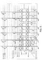
- FIG. 3 is an essential-portion circuit diagram showing a second embodiment of a configuration of a memory cell array 10 of the present invention device.
- the circuit diagram is described by using a memory cell of a mask ROM the same as the case of the first embodiment.
- the configuration in which the memory array 10 is divided into a plurality of subarrays 2 is the same as the case of the first embodiment and the configuration of the subarray 2 is completely the same as the case of the first embodiment.
- Specific modes of a hierarchical bit line system and first selection transistors BK1 and BK2 and second selection transistors BK 3, BK4 and BK5 are also the same as the case of the first embodiment.
- the second embodiment is different from the first embodiment in that four switching transistors EQ1 to EQ4 for electrically connecting two bit lines LB 1 and LB2 with three virtual ground lines LS1, LS2, and LS3 are set between those adjacent to each other.
- the switching transistor EQ1 is set between the virtual ground line LS1 and bit line LB1
- the switching transistor EQ2 is set between the virtual ground line LS3 and bit line LB2
- the switching transistor EQ3 is set between the virtual ground line LS2 and bit line LB1
- the switching transistor EQ4 is set between the virtual ground line LS2 and bit line LB2.
- the gate electrode of the switching transistor EQ1 is controlled by an EQ line B
- the gate electrode of the switching transistor EQ2 is controlled by an EQ line A
- gate electrodes of the switching transistors EQ3 and EQ4 are controlled by an EQ line C.
- Three control signal EQ lines A TO C are used for the four switching transistors EQ1 to EQ4.
- the EQ lines A and C are set to the high level simultaneously with the control of the first selection transistors BK1 and BK2 and second selection transistor BK3 to turn on the switching transistors EQ2 to EQ4.
- the virtual ground lines LS2 and LS3 are charged via the switching transistors EQ2 to EQ4 though they are charged via on-transistors when the memory cells M3 and M4 are the on-transistors. That is, in the case of this embodiment, charging bit lines is also applied to unselected virtual ground lines (virtual ground lines to be connected only to unselected memory cells) via the switching transistors EQ2 to EQ4 independently of storage states of the memory cells M3 and M4 or the potential level of a selected word line. Therefore, an alternate discharge current is more effectively restrained compared to the case of the first embodiment.
- the alternate discharge current does not cause a reading operation margin or reading operation speed to decrease because the above charging to unselected bit lines and virtual ground lines is performed from the global bit line GB the same as the case of the first embodiment.
- Selection of the memory cell M2 is the same as the case of the first embodiment also on the point of setting the block selection lines B and D or B, D, and E to the high level and turning on the first selection transistor BK1 and second selection transistor BK4 or BK4 and BK5.
- the control of the switching transistors EQ1 to EQ4, which is peculiar to the second embodiment is mainly described below.
- the EQ line B is set to the high level and the switching transistor EQ1 is turned on simultaneously with the control of the first selection transistor BK1 and second selection transistor BK4 or the transistors BK4 and BK5. Thereby, the unselected virtual ground line LS1 is also charged to the charging potential of the bit line LB1 through the switching transistor EQ1 and this charging more effectively prevents an alternate discharge current.
- EQ line A it is also allowed to set the EQ line A to the high level simultaneously with the EQ line B. This is because the selected virtual ground line LS2 is lowered to the ground potential, a charging operation or reading operation is not influenced even if the switching transistor EQ2 is turned on and the potential of the unselected bit line LB2 is lowered. Thereby, two EQ lines are set to the high level the same as the case of reading data from the memory cell M1 and it is possible to simplify control logics of the EQ lines.
- the case of reading data from the memory cell M3 is described.
- Selection of the memory cell M3 is the same as the case of the first embodiment.
- the point of setting the block selection lines A and D or A, D, and C to the high level and turning on the first selection transistor BK2 and second selection transistor BK4 or the transistors BK4 and BK3 is the same as the case of the first embodiment.
- the EQ line A is set to the high level to turn on the switching transistor EQ2 simultaneously with the control of the above block selection lines.
- the virtual ground line LS3 is also charged to the charging potential of the bit line LB2 through the switching transistor EQ2 and this charging more effectively prevents an alternate discharge current.
- the EQ lines B and C are set to the high level to turn on the switching transistors EQ1, EQ3, and EQ4 simultaneously with the control of the first selection transistors BK1 and BK2 and second selection transistor BK5.
- the virtual ground lines LS1 and LS2 are charged via the switching transistors EQ1, EQ3, and EQ4 though they are charged via on-transistors when the M1 and M2 are the on-transistors in the case of the first embodiment and thereby, an alternate discharge current is effectively restrained.
- This point is the same as reading data from the memory cell M1 which is bilaterally symmetrical to the virtual ground line LS2.
- the alternate injection current does not cause a reading operation margin or reading operation speed to decrease because charging unselected bit lines and virtual ground lines is the charging from the same global bit line GB.
- Reading data from the memory cells M1 to M4 is described above in accordance with Fig. 3.
- an operation margin is prevented from decreasing by also charging unselected bit lines and virtual ground lines.
- an operation margin is prevented from decreasing by charging unselected virtual ground lines through a switching transistor instead of charging unselected bit lines. In other words, it is determined to charge an unselected bit line or unselected virtual ground line in accordance with the position of a memory cell from which data will be read in the subarray 2.
- Fig. 4 shows a circuit configuration in which bit lines are replaced with virtual ground lines.
- a physical change of the connection between a transistor and each control signal is unnecessary.
- connections between the switching transistors EQ1 to EQ4 and their control signal EQ lines A to C are changed. Specifically, the EQ line B is unnecessary and the gate electrode of the switching transistor EQ1 is controlled by the EQ line A.
- the global line GB is replaced with the global virtual ground line GS by replacing the array of bit lines with that of virtual ground lines the same as the case of the first embodiment. Contrary, by replacing the global bit line GB with the global virtual ground line GS, the array of bit lines and that of virtual ground lines of the subarray 2 are replaced with each other. Because a reading operation is basically the same as the case of the configuration shown in Fig. 3, it is allowed to decide the control of the block selection lines A to E and switching transistors EQ1 to EQ4 for charging unselected bit lines and virtual ground lines according to the same concept.
- Fig. 5 is an essential-portion circuit diagram showing a third embodiment of the present invention.
- the third embodiment is constituted by adding a circuit for executing the short check (short-circuit test) between adjacent bit lines or adjacent virtual ground lines, which is performed in the fabrication process of a global bit line and global virtual ground line or a bit line and virtual ground line.
- the short check short-circuit test
- bit-line GNDA signal in Fig. 5 is set to the high level and the bit-line GNDB signal in Fig. 5 is set to the low level.
- a global bit line GB2 and global virtual ground lines GS1 and GS3 respectively have the ground potential.
- each block selection line, all word lines, and all EQ lines are set to the low level.
- a global virtual ground line GS2 is set to the VCC level (power supply potential) to measure the current flowing through the global virtual ground line GS2.
- bit line or the like an example of the short check of a bit line or virtual ground line (each of them is hereafter properly referred to as bit line or the like) is described below.
- bit line or the like The case of the short check of the virtual ground line LS3 is described.
- the bit-line GNDA signal in Fig. 5 is set to the low level to apply the VCC level to the global virtual ground line GS 1 from the outside.
- the bit-line GNDB signal in Fig. 5 is set to the high level so that the global bit line GB 1 and global virtual ground line GS2 becomes the ground potential.
- the block selection lines A and E are set to the high level.
- Other block selection lines all word lines, and all EQ lines are set to the low level.
- the current flowing through the global virtual ground line GS1 is measured.
- the bit line LB2 and virtual ground line LS4 become the ground potential and the virtual ground line LS3 becomes the VCC level. Therefore, when the virtual ground line LS3 shorts with the bit line LB2 or virtual ground line LS4, a short current flows. It is possible to execute the short check of all bit lines in accordance with the same concept.
- a transistor to be pulled down to the ground potential is connected to only a global line.
- Each of the above embodiments uses a memory cell of a mask ROM as a memory cell. However, it is also allowed to use a memory cell using a flash memory device or variable resistance device.
- Figs. 6 and 7 show equivalent circuit diagrams and typical sectional views of memory cells when using each element as a memory cell. In any case, a first electrode and a pair of second electrodes are used so that stored contents can be read in accordance with the state of electrical connection between the second electrodes correspondingly to the potential of the first electrode.
- the gate electrode of a MOSFET of a floating gate structure constituting a memory cell transistor corresponds to the first electrode
- the drain and source electrodes of the MOSFET correspond to the second electrodes respectively.
- the storage state of the memory cell is changed by transferring electrons to and from the floating gate and thereby controlling the threshold voltage of the memory cell transistor. It is allowed to control the threshold voltage by using the publicly-known programming-erasing technique of a flash memory.
- variable resistance device 5 when a memory cell using the variable resistance device 5 is used, one end of the variable resistance device 5 is connected with the drain electrode of a selection transistor 6 constituted by an n-channel MOSFET for selecting a memory cell, the gate electrode of the selection transistor 6 is used as a first electrode and the other end of the variable resistance device 5 and the source electrode of the selection transistor 6 are respectively used as a second electrode, and the second electrode at the variable resistance device 5 is connected to a bit line and the second electrode at the selection transistor 6 is connected to a virtual ground line. Change of the storage state of the memory cell is performed by changing the resistance value of the variable resistance device 5 in accordance with external control.
- variable resistance devices for performing the external control in accordance with an electrical stress
- a variable resistance device for performing the external control in accordance with a magnetic stress a variable resistance device for performing the external control in accordance with a thermal stress.
- an RRAM (Resistance control nonvolatile Random Access Memory) device is used as a variable resistance device whose resistance value is changed in accordance with an electrical stress (such as voltage pulse).
- the RRAM device is a nonvolatile memory device capable of storing data in accordance with the change of an electrical resistance because the electrical resistance is changed when an electrical stress is applied and a changed electrical resistance is kept after the electrical stress is canceled, which is fabricated by forming a manganese oxide film of any one of substances shown by Pr (1-x) Ca x MnO 3 , La (1-x) Cax MnO 3 , and La (1-x-y) Ca x Pb y MnO 3 (in this case, x ⁇ 1, y ⁇ 1, and x+y ⁇ 1) such as Pro 0.7 Ca 0.3 MnO 3 , La 0.65 Ca 0.35 MnO 3 , and La 0.65 Ca 0.175 Pb 0.175 MnO 3 in accordance with the MOCVD method, spin coating method, laser abrasion, or
- a memory cell from which data will be read by the present invention is a memory cell having one first electrode and a pair of second electrodes and capable of reading stored contents in accordance with the state of electrical connection between the second electrodes correspondingly to the potential of the first electrode.
- one of the two electrodes is fixedly connected to a bit line and the other of them is fixedly connected to a virtual ground line.
- a memory cell transistor has a structure in which the drain electrode and the source electrode are symmetric, a bit line and a virtual ground line are not functionally changed even if replacing them with each other because it is enough to fix either of the electrodes to the drain electrode and specify a one-directional reading current or it is necessary to fix one of the second electrodes to a bit line and the other of them to a virtual ground line because a memory cell has an asymmetric structure between the second electrodes.
- the configuration of a memory cell array of each of the above embodiments can be also used for a memory cell using a multi-bit memory device capable of independently supplying a reading current bidirectionally and the same advantage as that of each of the embodiments.
- a memory cell capable of storing two-bit data when a current flow direction differs whenever reading each one-bit data, it is possible to separately read two-bit data one bit by one bit by properly alternating a bit line and a virtual ground line.
- problems of the above alternate discharge current and alternate injection current similarly occur. According to the present invention, however, it is possible to avoid erroneous reading and decrease of an operation margin by excluding influences of these problems.
- An embodiment constituted by using a sidewall memory device is described below as a memory cell capable of storing two-bit data.
- a sidewall memory device 100 is a device constituted by a gate electrode 104 formed on a semiconductor layer 102 through a gate insulating film 103, a channel region 101 formed under the gate electrode 104, diffusion regions 105 and 106 formed at the both sides of the channel region 101 and having a conductivity type opposite to that of the channel region 101, and memory functional bodies 107 and 108 formed on the both sidewalls of the gate electrode 104 and respectively having a function for holding electric charges.
- Fig. 10B shows symbols of the sidewall memory device.
- a node G, node S, and node D denote the gate electrode 104, a source electrode 105, and a drain electrode 106 respectively and m1 and m2 denote memory functional bodies.
- a high voltage is applied to the gate G, a high voltage is applied to the node S, and the node D is set to the GND level to supply a current from the node S to the node D. Hot electrons thereby generated are injected into the memory functional body m1 and data is programmed.
- voltage conditions of the nodes S and D are reversed to change the current flowing direction from the node D to the node S.
- a voltage such as 3 V is applied to the node G and a voltage of 1.2 V is applied to the node D to set the node S to the GND level.
- a drain current easily flows.
- an inversion layer is not easily formed nearby the memory functional body m1 and the drain current does not easily flow.
- Fig. 11 shows the memory cell array configuration.
- the configuration of the memory cell array 20 shown in Fig. 11 is substantially the same as the configuration of the memory cell array 10 of the second embodiment shown in Fig. 3 but the configuration of the memory cell array 20 is different from that of the memory cell array 10 in that the memory device of the memory cell is replaced with a sidewall memory device.
- the function of a bit line is replaced with that of a virtual ground line depending on a memory functional body in one memory cell selected by a bit line or virtual ground line to be connected to the node S and node D. Therefore, in the case of the embodiment in Fig. 11, a bit line and a virtual ground line are not purposely differentiated but they are referred to as bit-source line.
- m1 and m2 of the memory cell M1 are memory functional bodies of a sidewall memory device.
- a case of applying the programming operation to the memory functional body m2 is described.
- the word line WL0 is first selectively set to a high-level voltage.
- a global bit-source line GBS1 is set to a high-level voltage and a global bit-source line GBS2 is set to the low level (GND level).
- the block selection lines A and B are set to the high level so that the first selection transistors BK1 and BK2 are turned on and the block selection line C is set to the high level so that the second selection transistor BK3 is turned on.
- an LEQ line A is set to the high level so that the switching transistor EQ2 is turned on and an LEQ line C is set to the high level so that the switching transistors EQ3 and EQ4 are turned on.
- the bit-source lines LBS2, LBS3, and LBS4, and LBS5 are set to the same potential by the switching transistors EQ3, EQ4, and EQ2 but no current flows through the memory cell M2, M3, or M4. Therefore, the programming operation is not applied to the memory cells.
- a block selection line and LEQ line are controlled the same as the case of the operation for programming data in the memory functional body m2.
- a current flows from the bit-source line LBS1 to the bit-source line LBS2 through the memory cell M1.
- electrons are injected into the memory functional body m1 and the programming operation is executed.
- the bit-source lines LBS2, LBS3, and LBS4 become the same potential at the GND level but no current flows through the memory cell M2, M3, or M4, the programming operation is not applied to the memory cells.
- data can be programmed in the memory functional body at the bit-source line LBS2 of the memory cell M2 by turning on the first selection transistor BK1, second selection transistors BK4 and BK5, and switching transistors EQ1 and EQ2 and setting the global bit-source line GBS1 to the high level, and the global bit-source line GBS2 to the GND level.
- data can be programmed in the memory functional body at the bit-source line LBS3 of the memory cell M2 by setting the global bit-source line GBS1 to the GND level and the global bit-source line GBS2 to the high level.
- the programming operation applied to the memory functional body at the bit-source line LBS2 of the memory cell M2 is different from the programming operation applied to the memory cell M2 only in that voltage conditions of the global bit-source lines GBS1 and GBS2 are reversed.
- Data can be programmed in the memory functional body at the bit-source line LBS3 of the memory cell M3 by turning on the first selection transistor BK2 and second selection transistors BK3 and BK4 and switching transistors EQ1 and EQ2 and setting the global bit-source line GBS1 to the GND level and the global bit-source line GBS2 to the high level.
- Data can be programmed in the memory functional body at the bit-source line LBS4 of the memory cell M3 by setting the global bit-source line GBS1 to the high level and the global bit-source line GBS2 to the GND level.
- the programming operation applied to the memory functional body of the memory cell M3 at the bit-source line LBS3 is different only in the voltage conditions of the global bit-source lines GBS1 and GBS2 are reversed.
- Data can be programmed in the memory functional body at the LBS4 of the memory cell M4 by turning on the first selection transistors BK1 and BK2, second selection transistor BK5, and switching transistors EQ1, EQ3, and EQ4 and setting the global bit-source line GBS1 to the high level and the global bit-source line GBS2 to the GND level.
- Data can be programmed in the memory functional body at the LBS5 of the memory cell M4 by setting the global bit-source line GBS1 to the GND level and the global bit-source line GBS2 to the high level.
- the programming operation applied to the memory functional body at the LBS4 of memory cell M4 is different only in the voltage conditions of the global bit-source lines GBS1 and GBS2 are reversed.
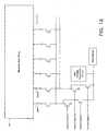
- Fig. 12 shows an example of circuit configuration of a circuit for supplying a high-level voltage and low-level voltage to the global bit-source lines GBS1 and GBS2 respectively.
- the control signals A and D By setting the control signals A and D to the high level and the controls signals B and C to the GND level, it is possible to set the global bit-source line GBS1 to the GND level and the global bit-source line GBS2 to the high level.
- Operations of the control signals A, B, C, and D can be realized by controlling them by address signals input to a semiconductor memory device. Moreover, it is possible to execute these controls at the same address in accordance with time sharing, that is, serial operation.
- the reading operation also makes it possible to read information from two memory functional bodies of a memory cell in accordance with the same procedure as the programming operation.
- high-level voltages to be applied to the global bit-source lines GBS1 and GBS2 word line WL, block selection lines A to E, and LEQ lines A to C are voltages most suitable for operations of the lines respectively.
- the present invention it is possible to increase the number of memory cells from which data will be read onto the same word line compared to the case of a conventional memory cell array configuration. Moreover, the present invention can be effectively used as an advanced memory array configuration for reading data from a lot of memory cells through one-time reading operation and performing the subsequent reading operation at a high speed.
Landscapes
- Engineering & Computer Science (AREA)
- Business, Economics & Management (AREA)
- Chemical & Material Sciences (AREA)
- Materials Engineering (AREA)
- Educational Administration (AREA)
- Educational Technology (AREA)
- Theoretical Computer Science (AREA)
- General Physics & Mathematics (AREA)
- Physics & Mathematics (AREA)
- Strategic Management (AREA)
- Tourism & Hospitality (AREA)
- Microelectronics & Electronic Packaging (AREA)
- Computer Hardware Design (AREA)
- Economics (AREA)
- Primary Health Care (AREA)
- General Business, Economics & Management (AREA)
- Marketing (AREA)
- Human Resources & Organizations (AREA)
- General Health & Medical Sciences (AREA)
- Health & Medical Sciences (AREA)
- Read Only Memory (AREA)
- Semiconductor Memories (AREA)
Abstract
Description
Claims (21)
- A semiconductor memory device comprising;in which said memory cell array is constituted by connecting the first electrodes of said memory cells in the same row to a common word line, connecting said second electrodes each other between two of said memory cells adjacent to each other in the row direction, connecting one-hand said second electrodes in said memory cells in the same column to a common bit line, and connecting the other-hand said second electrodes in said memory cells in the same column to a common virtual ground line, characterized in thata memory cell array in which memory cells respectively having one first electrode and a pair of second electrodes and capable of reading stored contents correspondingly to the potential of said first electrode in accordance with a state of the electrical connection between said second electrodes are arranged in the row and the column directions like a matrix,
said memory cell array is constituted by being divided into at least a plurality columns of subarrays,
memory cell columns at the both ends of said subarrays are constituted so that said second electrodes are not connected each other between two of said memory cells adjacent to each other in the row direction at the both sides of boundaries between said subarrays but they are separated from each other and respectively connected to an independent bit line or virtual ground line, and
one of said word lines, one of said bit lines, and one of said virtual ground lines are selected for each of said subarrays and one memory cell from which data will be read is selected. - A semiconductor memory device comprising a memory cell array in which memory cells respectively having one first electrode and a pair of second electrodes and capable of reading stored contents correspondingly to the potential of said first electrode in accordance with a state of the electrical connection between said second electrodes are arranged in the row and the column directions like a matrix and said memory cell array is constituted by connecting the first electrodes of said memory cells in the same row to a common word line, connecting said second electrodes each other between two of said memory cells adjacent in the row direction, connecting one-hand said second electrodes in said memory cells in the same column to a common bit line, and connecting the other-hand said second electrodes in said memory cells in the same column to a common virtual ground line, characterized in that
said memory cell array is constituted by being divided into at least a plurality columns of subarrays,
memory cell columns at the both ends of said subarrays are constituted so that
said second electrodes are not connected each other between two of said memory cells adjacent to each other in the row direction at the both sides of boundaries between said subarrays but they are separated from each other and respectively connected to an independent bit line or virtual ground line, and
each of said bit lines and each of said virtual ground lines respectively have functions of the both and when one of them executes the function of the other while the other executes the function of the former. - The semiconductor memory device according to claim 1, characterized in that
each of said bit lines and each of said virtual ground lines respectively have functions of the both and when one of them executes the function of the other, the other executes the function of the former. - The semiconductor memory device according to claim 1, characterized in that
the number of columns of said memory cells constituting said subarrays is 4. - The semiconductor memory device according to claim 1, characterized in that
said bit lines are connected to a common global bit line through a first selection transistor and said virtual ground lines are connected to a common global virtual ground line through a second selection transistor for each of said subarrays. - The semiconductor memory device according to claim 1, characterized in that
a charging circuit is included which supplies a predetermined charging voltage to some or all of said bit lines and virtual ground lines of said subarrays in order to execute the reading operation. - The semiconductor memory device according to claim 6, characterized in that
said bit lines are connected to a common global bit line through a first selection transistor and said virtual ground lines are connected to a common global virtual ground line through a second selection transistor, and
said charging circuit charges said bit lines and said virtual ground lines to be charged through said global bit line and said global virtual ground line. - The semiconductor memory device according to claim 7, characterized in that in said subarrays including said memory cells from which data will be read,
at least one of said bit lines and one of said virtual ground lines to be connected only to said memory cells from which data will not be read are included as one of said bit lines and one of said virtual ground lines to be charged correspondingly to positions of said memory cells from which data will be read in said subarrays, and
said charging circuit charges said bit lines and said virtual ground lines to be charged at the time of the reading operation. - The semiconductor memory device according to claim 7, characterized in that in said subarrays including said memory cells from which data will be read,
at least one of said bit lines and one of said virtual ground lines to be connected only to said memory cells from which data will not be read are included as one of said bit lines and one of said virtual ground lines to be charged correspondingly to positions of said memory cells from which data will be read in said subarrays, and
said charging circuit charges said bit lines and said virtual ground lines to be charged during a charging period following the reading operation. - The semiconductor memory device according to claim 1, characterized in that
a switching transistor is set between said bit lines and said virtual ground lines adjacent to each other in said subarrays. - The semiconductor memory device according to claim 10, characterized in that
the number of columns of said memory cells constituting said subarrays is 4 and two out of four of said switching transistors set to each of said subarrays are controlled in common and two other switching transistors are controlled independently. - The semiconductor memory device according to claim 10, characterized in that in said subarrays including said memory cells from which data will be read,
said switching transistors set between said bit lines and said virtual ground lines to be connected to said memory cells from which data will be read are turned off at the time of the reading operation. - The semiconductor memory device according to claim 10, characterized in that in said subarrays including said memory cells from which data will be read,
said switching transistors set between said bit lines and said virtual ground lines to be connected to said memory cells from which data will be read are turned off during a charging period following the reading operation. - The semiconductor memory device according to claim 1, characterized in that
said bit lines are connected to a common global bit line through a first selection transistor and said virtual ground lines are connected to a common global virtual ground line through a second selection transistor, and
a grounding switch transistor to be electrically connected with a ground line is set to said global bit line and said global virtual ground line respectively. - The semiconductor memory device according to claim 1, characterized in that
said bit lines are connected to a common global bit line through a first selection transistor and said virtual ground lines are connected to a common global virtual ground line through a second selection transistor for each of said subarrays, and
two of said first selection transistor or two of said second selection transistor to be connected to said bit line or said virtual ground line adjacent to each other at the both sides of boundaries between said subarrays are respectively controlled by a common control signal. - The semiconductor memory device according to claim 1, characterized in that
said memory cells are respectively constituted by a flash memory device or variable resistance device. - The semiconductor memory device according to claim 1, characterized in that
said memory cells respectively have a MOSFET structure and are respectively constituted by a sidewall memory device having a memory functional body on the sidewall of at least either of the drain side and source side for a gate. - The semiconductor memory device according to claim 17, characterized in that
a circuit for supplying programming voltages different from each other and said memory cell array are constituted so that the voltages can be applied to said bit lines and said virtual ground lines to be connected to said memory cells in which data will be programmed for programming operations of said memory cells in said subarrays. - The semiconductor memory device according to claim 18, characterized in that said sidewall memory device;
has a memory functional body at the both of the drain side and source side to a gate,
controls voltages to be applied to said bit lines and said virtual ground lines to be connected to said selected memory cells in accordance with a memory-functional-body selection signal for selecting either of said memory functional bodies in said memory cells, and
applies the programming operation or reading operation to said two memory functional bodies respectively by changing current directions for said selected memory cells in accordance with said voltage control. - The semiconductor memory device according to claim 19, characterized in that
said memory-functional-body selection signal serves as a part of an address signal. - The semiconductor memory device according to claim 19, characterized in that by selecting one of said memory cells and changing said memory-functional-body selection signal,
a voltage to be applied to said bit lines and said virtual ground lines to be connected to said selected memory cells is reversed before and after the change of said memory-functional-body selection signal to continuously apply the programming operation or reading operation to said two memory functional bodies of said selected memory cells.
Applications Claiming Priority (4)
| Application Number | Priority Date | Filing Date | Title |
|---|---|---|---|
| JP2003022805 | 2003-01-30 | ||
| JP2003022805 | 2003-01-30 | ||
| JP2003433814A JP2004253115A (en) | 2003-01-30 | 2003-12-26 | Semiconductor storage device |
| JP2003433814 | 2003-12-26 |
Publications (2)
| Publication Number | Publication Date |
|---|---|
| EP1443520A2 true EP1443520A2 (en) | 2004-08-04 |
| EP1443520A3 EP1443520A3 (en) | 2006-07-19 |
Family
ID=32658606
Family Applications (1)
| Application Number | Title | Priority Date | Filing Date |
|---|---|---|---|
| EP04250463A Withdrawn EP1443520A3 (en) | 2003-01-30 | 2004-01-28 | Semiconductor memory device |
Country Status (6)
| Country | Link |
|---|---|
| US (1) | US6920058B2 (en) |
| EP (1) | EP1443520A3 (en) |
| JP (1) | JP2004253115A (en) |
| KR (1) | KR100534834B1 (en) |
| CN (1) | CN100440369C (en) |
| TW (1) | TWI240283B (en) |
Families Citing this family (21)
| Publication number | Priority date | Publication date | Assignee | Title |
|---|---|---|---|---|
| KR100416599B1 (en) * | 2001-05-31 | 2004-02-05 | 삼성전자주식회사 | Memory cell structure of metal programmable ROM capable of improving memory density and read speed and reducing power consumption |
| US7042750B2 (en) * | 2002-07-18 | 2006-05-09 | Samsung Electronics Co., Ltd. | Read only memory devices with independently precharged virtual ground and bit lines |
| JP2005327339A (en) * | 2004-05-12 | 2005-11-24 | Matsushita Electric Ind Co Ltd | Mask ROM |
| FR2881565B1 (en) * | 2005-02-03 | 2007-08-24 | Atmel Corp | BINARY LINE SELECTION CIRCUITS FOR NON-VOLATILE MEMORIES |
| JP2006302436A (en) * | 2005-04-22 | 2006-11-02 | Matsushita Electric Ind Co Ltd | Semiconductor memory device |
| US8400841B2 (en) * | 2005-06-15 | 2013-03-19 | Spansion Israel Ltd. | Device to program adjacent storage cells of different NROM cells |
| KR100960208B1 (en) * | 2005-07-29 | 2010-05-27 | 후지쯔 가부시끼가이샤 | Resistance Memory and Nonvolatile Semiconductor Memory |
| US7376013B2 (en) * | 2005-09-29 | 2008-05-20 | Virage Logic Corp. | Compact virtual ground diffusion programmable ROM array architecture, system and method |
| JP4392404B2 (en) | 2005-12-07 | 2010-01-06 | シャープ株式会社 | Virtual ground type nonvolatile semiconductor memory device |
| US7391664B2 (en) * | 2006-04-27 | 2008-06-24 | Ovonyx, Inc. | Page mode access for non-volatile memory arrays |
| JP4809170B2 (en) * | 2006-09-20 | 2011-11-09 | シャープ株式会社 | Semiconductor memory device and electronic device |
| JP5052991B2 (en) * | 2007-05-21 | 2012-10-17 | ラピスセミコンダクタ株式会社 | Memory cell array and semiconductor memory device |
| WO2008148091A1 (en) * | 2007-05-25 | 2008-12-04 | Marvell World Trade Ltd. | Tree type bit line decoder architecture for nor-type memory array |
| JP2010055734A (en) * | 2008-07-31 | 2010-03-11 | Panasonic Corp | Semiconductor memory device |
| US7961490B2 (en) * | 2009-01-09 | 2011-06-14 | Arm Limited | Generating ROM bit cell arrays |
| TWI424443B (en) * | 2009-05-08 | 2014-01-21 | Macronix Int Co Ltd | Memory array and method of operating a memory |
| JP2012204399A (en) * | 2011-03-23 | 2012-10-22 | Toshiba Corp | Resistance change memory |
| CN102969024A (en) * | 2011-09-01 | 2013-03-13 | 成都海存艾匹科技有限公司 | Self-repair system and method |
| KR101607616B1 (en) * | 2015-05-15 | 2016-03-30 | 부경대학교 산학협력단 | Method for switching memory resistor |
| US10127990B1 (en) * | 2017-07-18 | 2018-11-13 | Stmicroelectronics International N.V. | Non-volatile memory (NVM) with dummy rows supporting memory operations |
| US11348628B2 (en) * | 2020-09-25 | 2022-05-31 | Nxp Usa, Inc. | Non-volatle memory with virtual ground voltage provided to unselected column lines during memory read operation |
Family Cites Families (10)
| Publication number | Priority date | Publication date | Assignee | Title |
|---|---|---|---|---|
| US4460981A (en) * | 1981-12-24 | 1984-07-17 | Intel Corporation | Virtual ground memory |
| US4594689A (en) * | 1984-09-04 | 1986-06-10 | Motorola, Inc. | Circuit for equalizing bit lines in a ROM |
| WO1996008821A1 (en) * | 1994-09-13 | 1996-03-21 | Macronix International Co., Ltd. | Flash eprom integrated circuit architecture |
| JP3739104B2 (en) * | 1995-02-27 | 2006-01-25 | 株式会社ルネサステクノロジ | Nonvolatile semiconductor memory device |
| JPH09231783A (en) * | 1996-02-26 | 1997-09-05 | Sharp Corp | Semiconductor memory device |
| JP2882370B2 (en) | 1996-06-28 | 1999-04-12 | 日本電気株式会社 | Semiconductor storage device |
| JPH118324A (en) * | 1997-04-23 | 1999-01-12 | Sanyo Electric Co Ltd | Transistor, transistor array and nonvolatile semiconductor memory |
| KR100252475B1 (en) * | 1997-05-24 | 2000-04-15 | 윤종용 | Semiconductor rom |
| JP3583042B2 (en) * | 1999-11-09 | 2004-10-27 | Necエレクトロニクス株式会社 | Semiconductor storage device |
| US6542412B2 (en) * | 2000-09-06 | 2003-04-01 | Halo Lsi, Inc. | Process for making and programming and operating a dual-bit multi-level ballistic flash memory |
-
2003
- 2003-12-26 JP JP2003433814A patent/JP2004253115A/en active Pending
-
2004
- 2004-01-28 EP EP04250463A patent/EP1443520A3/en not_active Withdrawn
- 2004-01-30 TW TW093102193A patent/TWI240283B/en not_active IP Right Cessation
- 2004-01-30 CN CNB2004100025749A patent/CN100440369C/en not_active Expired - Lifetime
- 2004-01-30 US US10/769,381 patent/US6920058B2/en not_active Expired - Lifetime
- 2004-01-30 KR KR10-2004-0005999A patent/KR100534834B1/en not_active Expired - Fee Related
Also Published As
| Publication number | Publication date |
|---|---|
| KR20040070079A (en) | 2004-08-06 |
| TWI240283B (en) | 2005-09-21 |
| TW200423151A (en) | 2004-11-01 |
| KR100534834B1 (en) | 2005-12-08 |
| US6920058B2 (en) | 2005-07-19 |
| US20040184318A1 (en) | 2004-09-23 |
| CN100440369C (en) | 2008-12-03 |
| CN1558421A (en) | 2004-12-29 |
| JP2004253115A (en) | 2004-09-09 |
| EP1443520A3 (en) | 2006-07-19 |
Similar Documents
| Publication | Publication Date | Title |
|---|---|---|
| EP1443520A2 (en) | Semiconductor memory device | |
| US7239571B2 (en) | Semiconductor memory device | |
| EP1235229B1 (en) | Method of read operation of nonvolatile semiconductor memory and nonvolatile semiconductor memory | |
| JP4355136B2 (en) | Nonvolatile semiconductor memory device and reading method thereof | |
| US6914813B2 (en) | Segmented non-volatile memory array with multiple sources having improved source line decode circuitry | |
| US8085615B2 (en) | Multi-state resistance changing memory with a word line driver for applying a same program voltage to the word line | |
| US5625586A (en) | Semiconductor memory having a plurality of memory banks and sub-bit lines which are connected to a main bit line via MOS transistors whose gates are commonly connected to a selection line | |
| US9230640B2 (en) | Ground circuitry for semiconductor memory device | |
| KR100749673B1 (en) | Nonvolatile semiconductor memory | |
| US7911864B2 (en) | Semiconductor memory device | |
| US10192616B2 (en) | Ovonic threshold switch (OTS) driver/selector uses unselect bias to pre-charge memory chip circuit and reduces unacceptable false selects | |
| KR100491912B1 (en) | Nonvolatile semiconductor memory | |
| US20080175035A1 (en) | Non-volatile resistance changing for advanced memory applications | |
| JP4189269B2 (en) | Nonvolatile semiconductor memory device, write / reset method thereof, and read method thereof | |
| US6185131B1 (en) | Nonvolatile semiconductor storage device capable of electrically isolating dummy cell array region from memory cell array region | |
| US7184318B2 (en) | Semiconductor memory device | |
| US7630243B2 (en) | Semiconductor memory device | |
| EP0978844B1 (en) | Sensing arrangement for a multilevel semiconductor memory device | |
| CN118136061A (en) | A high-density storage array | |
| EP4243022B1 (en) | Memory cell and array structure of non-volatile memory | |
| WO2009075832A1 (en) | Nonvolatile storage device and control method thereof | |
| US6940755B2 (en) | Semiconductor with an improved read device and operational mode associated therewith | |
| JP2025143024A (en) | storage device | |
| JP2000285689A (en) | Semiconductor storage device |
Legal Events
| Date | Code | Title | Description |
|---|---|---|---|
| PUAI | Public reference made under article 153(3) epc to a published international application that has entered the european phase |
Free format text: ORIGINAL CODE: 0009012 |
|
| AK | Designated contracting states |
Kind code of ref document: A2 Designated state(s): AT BE BG CH CY CZ DE DK EE ES FI FR GB GR HU IE IT LI LU MC NL PT RO SE SI SK TR |
|
| AX | Request for extension of the european patent |
Extension state: AL LT LV MK |
|
| PUAL | Search report despatched |
Free format text: ORIGINAL CODE: 0009013 |
|
| AK | Designated contracting states |
Kind code of ref document: A3 Designated state(s): AT BE BG CH CY CZ DE DK EE ES FI FR GB GR HU IE IT LI LU MC NL PT RO SE SI SK TR |
|
| AX | Request for extension of the european patent |
Extension state: AL LT LV MK |
|
| RIC1 | Information provided on ipc code assigned before grant |
Ipc: G11C 17/12 20060101ALI20060613BHEP Ipc: G11C 16/26 20060101ALI20060613BHEP Ipc: G11C 16/04 20060101AFI20040422BHEP |
|
| 17P | Request for examination filed |
Effective date: 20060922 |
|
| AKX | Designation fees paid |
Designated state(s): DE FR GB IT |
|
| 17Q | First examination report despatched |
Effective date: 20071123 |
|
| STAA | Information on the status of an ep patent application or granted ep patent |
Free format text: STATUS: THE APPLICATION IS DEEMED TO BE WITHDRAWN |
|
| 18D | Application deemed to be withdrawn |
Effective date: 20080604 |