EP1443488A1 - Improved drive scheme for cholesteric liquid crystal displays - Google Patents
Improved drive scheme for cholesteric liquid crystal displays Download PDFInfo
- Publication number
- EP1443488A1 EP1443488A1 EP03079141A EP03079141A EP1443488A1 EP 1443488 A1 EP1443488 A1 EP 1443488A1 EP 03079141 A EP03079141 A EP 03079141A EP 03079141 A EP03079141 A EP 03079141A EP 1443488 A1 EP1443488 A1 EP 1443488A1
- Authority
- EP
- European Patent Office
- Prior art keywords
- drive scheme
- state
- voltage
- row
- selection time
- Prior art date
- Legal status (The legal status is an assumption and is not a legal conclusion. Google has not performed a legal analysis and makes no representation as to the accuracy of the status listed.)
- Withdrawn
Links
- 239000004986 Cholesteric liquid crystals (ChLC) Substances 0.000 title claims description 25
- 238000009432 framing Methods 0.000 claims abstract description 10
- 239000004973 liquid crystal related substance Substances 0.000 claims abstract description 10
- 230000007547 defect Effects 0.000 claims abstract description 9
- 230000001419 dependent effect Effects 0.000 claims abstract description 9
- 239000011159 matrix material Substances 0.000 claims abstract description 3
- 238000002360 preparation method Methods 0.000 claims description 5
- 239000000463 material Substances 0.000 description 31
- 238000010586 diagram Methods 0.000 description 23
- 239000004020 conductor Substances 0.000 description 22
- 230000003098 cholesteric effect Effects 0.000 description 15
- 229920000642 polymer Polymers 0.000 description 6
- 239000000758 substrate Substances 0.000 description 6
- 230000005684 electric field Effects 0.000 description 4
- 238000000034 method Methods 0.000 description 4
- 101150100678 Pon1 gene Proteins 0.000 description 3
- 101150043906 Pon2 gene Proteins 0.000 description 3
- 101150098895 Pon3 gene Proteins 0.000 description 3
- 229910052751 metal Inorganic materials 0.000 description 3
- 239000002184 metal Substances 0.000 description 3
- OKTJSMMVPCPJKN-UHFFFAOYSA-N Carbon Chemical compound [C] OKTJSMMVPCPJKN-UHFFFAOYSA-N 0.000 description 2
- 108010010803 Gelatin Proteins 0.000 description 2
- PXHVJJICTQNCMI-UHFFFAOYSA-N Nickel Chemical compound [Ni] PXHVJJICTQNCMI-UHFFFAOYSA-N 0.000 description 2
- 229920003171 Poly (ethylene oxide) Polymers 0.000 description 2
- 239000004372 Polyvinyl alcohol Substances 0.000 description 2
- 229910052782 aluminium Inorganic materials 0.000 description 2
- XAGFODPZIPBFFR-UHFFFAOYSA-N aluminium Chemical compound [Al] XAGFODPZIPBFFR-UHFFFAOYSA-N 0.000 description 2
- 238000000576 coating method Methods 0.000 description 2
- 230000006870 function Effects 0.000 description 2
- 229920000159 gelatin Polymers 0.000 description 2
- 239000008273 gelatin Substances 0.000 description 2
- 235000019322 gelatine Nutrition 0.000 description 2
- 235000011852 gelatine desserts Nutrition 0.000 description 2
- AMGQUBHHOARCQH-UHFFFAOYSA-N indium;oxotin Chemical compound [In].[Sn]=O AMGQUBHHOARCQH-UHFFFAOYSA-N 0.000 description 2
- 239000000976 ink Substances 0.000 description 2
- 238000010329 laser etching Methods 0.000 description 2
- BASFCYQUMIYNBI-UHFFFAOYSA-N platinum Chemical compound [Pt] BASFCYQUMIYNBI-UHFFFAOYSA-N 0.000 description 2
- 229920000728 polyester Polymers 0.000 description 2
- 229920002451 polyvinyl alcohol Polymers 0.000 description 2
- XOLBLPGZBRYERU-UHFFFAOYSA-N tin dioxide Chemical compound O=[Sn]=O XOLBLPGZBRYERU-UHFFFAOYSA-N 0.000 description 2
- 229910001887 tin oxide Inorganic materials 0.000 description 2
- RYGMFSIKBFXOCR-UHFFFAOYSA-N Copper Chemical compound [Cu] RYGMFSIKBFXOCR-UHFFFAOYSA-N 0.000 description 1
- ZOKXTWBITQBERF-UHFFFAOYSA-N Molybdenum Chemical compound [Mo] ZOKXTWBITQBERF-UHFFFAOYSA-N 0.000 description 1
- 101100114417 Neurospora crassa (strain ATCC 24698 / 74-OR23-1A / CBS 708.71 / DSM 1257 / FGSC 987) con-13 gene Proteins 0.000 description 1
- BQCADISMDOOEFD-UHFFFAOYSA-N Silver Chemical compound [Ag] BQCADISMDOOEFD-UHFFFAOYSA-N 0.000 description 1
- ATJFFYVFTNAWJD-UHFFFAOYSA-N Tin Chemical compound [Sn] ATJFFYVFTNAWJD-UHFFFAOYSA-N 0.000 description 1
- 239000007864 aqueous solution Substances 0.000 description 1
- 239000007900 aqueous suspension Substances 0.000 description 1
- 238000000149 argon plasma sintering Methods 0.000 description 1
- 239000011230 binding agent Substances 0.000 description 1
- 229910052799 carbon Inorganic materials 0.000 description 1
- 239000011248 coating agent Substances 0.000 description 1
- 229920001688 coating polymer Polymers 0.000 description 1
- 150000001875 compounds Chemical class 0.000 description 1
- 229910052802 copper Inorganic materials 0.000 description 1
- 239000010949 copper Substances 0.000 description 1
- 230000000694 effects Effects 0.000 description 1
- 238000010894 electron beam technology Methods 0.000 description 1
- 230000005284 excitation Effects 0.000 description 1
- 239000011521 glass Substances 0.000 description 1
- 229910002804 graphite Inorganic materials 0.000 description 1
- 239000010439 graphite Substances 0.000 description 1
- 238000010438 heat treatment Methods 0.000 description 1
- 229910052738 indium Inorganic materials 0.000 description 1
- APFVFJFRJDLVQX-UHFFFAOYSA-N indium atom Chemical compound [In] APFVFJFRJDLVQX-UHFFFAOYSA-N 0.000 description 1
- 238000004519 manufacturing process Methods 0.000 description 1
- 238000005259 measurement Methods 0.000 description 1
- 239000007769 metal material Substances 0.000 description 1
- 150000002739 metals Chemical class 0.000 description 1
- 239000000203 mixture Substances 0.000 description 1
- 229910052750 molybdenum Inorganic materials 0.000 description 1
- 239000011733 molybdenum Substances 0.000 description 1
- 229910052759 nickel Inorganic materials 0.000 description 1
- 230000003287 optical effect Effects 0.000 description 1
- 239000002245 particle Substances 0.000 description 1
- 229920003023 plastic Polymers 0.000 description 1
- 239000004033 plastic Substances 0.000 description 1
- 229910052697 platinum Inorganic materials 0.000 description 1
- 230000010287 polarization Effects 0.000 description 1
- 239000004417 polycarbonate Substances 0.000 description 1
- 229920000515 polycarbonate Polymers 0.000 description 1
- 229920006267 polyester film Polymers 0.000 description 1
- 238000002310 reflectometry Methods 0.000 description 1
- 230000004044 response Effects 0.000 description 1
- 229910052709 silver Inorganic materials 0.000 description 1
- 239000004332 silver Substances 0.000 description 1
- 238000004544 sputter deposition Methods 0.000 description 1
- 229920005992 thermoplastic resin Polymers 0.000 description 1
- 229910052718 tin Inorganic materials 0.000 description 1
- 239000011135 tin Substances 0.000 description 1
- WFKWXMTUELFFGS-UHFFFAOYSA-N tungsten Chemical compound [W] WFKWXMTUELFFGS-UHFFFAOYSA-N 0.000 description 1
- 229910052721 tungsten Inorganic materials 0.000 description 1
- 239000010937 tungsten Substances 0.000 description 1
Images









Classifications
-
- G—PHYSICS
- G09—EDUCATION; CRYPTOGRAPHY; DISPLAY; ADVERTISING; SEALS
- G09G—ARRANGEMENTS OR CIRCUITS FOR CONTROL OF INDICATING DEVICES USING STATIC MEANS TO PRESENT VARIABLE INFORMATION
- G09G3/00—Control arrangements or circuits, of interest only in connection with visual indicators other than cathode-ray tubes
- G09G3/20—Control arrangements or circuits, of interest only in connection with visual indicators other than cathode-ray tubes for presentation of an assembly of a number of characters, e.g. a page, by composing the assembly by combination of individual elements arranged in a matrix no fixed position being assigned to or needed to be assigned to the individual characters or partial characters
- G09G3/34—Control arrangements or circuits, of interest only in connection with visual indicators other than cathode-ray tubes for presentation of an assembly of a number of characters, e.g. a page, by composing the assembly by combination of individual elements arranged in a matrix no fixed position being assigned to or needed to be assigned to the individual characters or partial characters by control of light from an independent source
- G09G3/36—Control arrangements or circuits, of interest only in connection with visual indicators other than cathode-ray tubes for presentation of an assembly of a number of characters, e.g. a page, by composing the assembly by combination of individual elements arranged in a matrix no fixed position being assigned to or needed to be assigned to the individual characters or partial characters by control of light from an independent source using liquid crystals
- G09G3/3611—Control of matrices with row and column drivers
- G09G3/3622—Control of matrices with row and column drivers using a passive matrix
- G09G3/3629—Control of matrices with row and column drivers using a passive matrix using liquid crystals having memory effects, e.g. ferroelectric liquid crystals
-
- G—PHYSICS
- G09—EDUCATION; CRYPTOGRAPHY; DISPLAY; ADVERTISING; SEALS
- G09G—ARRANGEMENTS OR CIRCUITS FOR CONTROL OF INDICATING DEVICES USING STATIC MEANS TO PRESENT VARIABLE INFORMATION
- G09G2300/00—Aspects of the constitution of display devices
- G09G2300/04—Structural and physical details of display devices
- G09G2300/0469—Details of the physics of pixel operation
- G09G2300/0478—Details of the physics of pixel operation related to liquid crystal pixels
- G09G2300/0482—Use of memory effects in nematic liquid crystals
- G09G2300/0486—Cholesteric liquid crystals, including chiral-nematic liquid crystals, with transitions between focal conic, planar, and homeotropic states
-
- G—PHYSICS
- G09—EDUCATION; CRYPTOGRAPHY; DISPLAY; ADVERTISING; SEALS
- G09G—ARRANGEMENTS OR CIRCUITS FOR CONTROL OF INDICATING DEVICES USING STATIC MEANS TO PRESENT VARIABLE INFORMATION
- G09G2310/00—Command of the display device
- G09G2310/06—Details of flat display driving waveforms
- G09G2310/065—Waveforms comprising zero voltage phase or pause
-
- G—PHYSICS
- G09—EDUCATION; CRYPTOGRAPHY; DISPLAY; ADVERTISING; SEALS
- G09G—ARRANGEMENTS OR CIRCUITS FOR CONTROL OF INDICATING DEVICES USING STATIC MEANS TO PRESENT VARIABLE INFORMATION
- G09G2320/00—Control of display operating conditions
- G09G2320/02—Improving the quality of display appearance
- G09G2320/0204—Compensation of DC component across the pixels in flat panels
Definitions
- the present invention relates to cholesteric (chiral nematic) liquid crystal displays and their electrical drive schemes, and more particularly to such a drive scheme which eliminates data dependent defects.
- US 5,437,811 issued August 1, 1995 to Doane et al. discloses a light-modulating cell having a chiral nematic liquid crystal (cholesteric liquid crystal) in polymeric domains contained by conventional patterned glass substrates.
- the chiral nematic liquid crystal has the property of being driven between a planar state reflecting a specific visible wavelength of light and a light scattering focal conic state.
- Chiral nematic material has two stable states and can maintain one of the stable states in the absence of an electric field.
- a drive scheme for driving the pixels of a passive matrix liquid crystal display having row and column electrodes including a selection step, the selection step including applying row and column waveforms to the display to generate selected pixel voltage pulses in a selected row and to generate non selected pixel voltage pulses in non selected rows, the selection step having an effective selection time that depends on the preceding and following nonselected pixel voltages, wherein a framing voltage pulse is inserted between each successive selected pixel voltage pulse such that the effective selection time is independent of the preceding and following nonselected pixel voltages, whereby data pattern dependent defects in a displayed image are eliminated.
- the drive scheme of the present invention has the advantage that it produces a uniform display state for each pixel in the display independent of the display state of neighboring pixels.
- the present invention has the further advantage that it can be applied to a variety of dynamic drive schemes including the U / 2 and U / 3/2 dynamic drive schemes and a variety of other fast drive schemes known in the art.
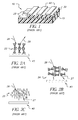
- Fig. 1 is partial perspective view of a structure for a prior art display 10 that can be driven in accordance with the invention.
- Display 10 includes a flexible substrate 15 , which is a thin transparent polymeric material, such as Kodak EstarTM film base formed of polyester plastic that has a thickness of between 20 and 200 microns.
- a substrate 15 can be a 125 micron thick sheet of polyester film base.
- Other polymers, such as transparent polycarbonate, can also be used.
- Electrodes in the form of first patterned conductors 20 are formed over substrate 15.
- First patterned conductors 20 can be tin-oxide or indium-tin-oxide (ITO), with ITO being the preferred material.
- the material of first patterned conductors 20 is sputtered as a layer over substrate 15 having a resistance of less than 250 ohms per square. The layer is then patterned to form first patterned conductors 20 in any well known manner.
- first patterned conductors 20 can be an opaque electrical conductor material such as copper, aluminum, or nickel. If first patterned conductors 20 are opaque metal, the metal can be oxidized to create light absorbing first patterned conductors 20 .
- First patterned conductors 20 are formed in the conductive layer by conventional photolithographic or laser etching means.
- a light modulating material such as a polymer dispersed cholesteric layer 30 overlays first patterned conductors 20.
- the polymer dispersed cholesteric layer 30 includes a polymeric host material and dispersed cholesteric liquid crystal materials, such as those disclosed in US 5,695,682 issued December 9, 1997 to Doane et al., the disclosure of which is incorporated by reference.
- Application of electrical fields of various amplitude and duration can drive a chiral nematic material into a reflective state, a transmissive state, or an intermediate state.
- These cholesteric materials have the advantage of maintaining a given state indefinitely after the field is removed.
- Cholesteric liquid crystal materials can be Merck BL112, BL118 or BL126, available from E.M. Industries of Hawthorne, NY.
- the polymeric host material is provided by E.M. Industries cholesteric material BL-118 dispersed in deionized photographic gelatin.
- the liquid crystal material is dispersed at 8% concentration in a 5% deionized gelatin aqueous solution.
- the mixture is dispersed to create 10 micron diameter domains of the liquid crystal in aqueous suspension.
- the material is coated over a patterned ITO polyester sheet to provide a 7 micron thick polymer dispersed cholesteric coating.
- Other organic binders such as polyvinyl alcohol (PVA) or polyethylene oxide (PEO) can be used. Such compounds are machine coatable on equipment associated with photographic films.
- Electrodes in the form of second patterned conductors 40 overlay polymer dispersed cholesteric layer 30.
- Second patterned conductors 40 should have sufficient conductivity to establish an electric field across polymer dispersed cholesteric layer 30 .
- Second patterned conductors 40 can be formed in a vacuum environment using materials such as aluminum, silver, platinum, carbon, tungsten, molybdenum, tin, or indium or combinations thereof.
- the second patterned conductors 40 are as shown in the form of a deposited layer. Oxides of the metals can be used to darken second patterned conductors 40.
- the metal material can be oxidized by applying energy from resistance heating, cathodic arc, electron beam, sputtering, or magnetron excitation.
- Tin-oxide or indium-tin-oxide coatings permit second patterned conductors 40 to be transparent. Electrodes 20 and 40 are on opposite sides of the layer 30 and are in rows and columns, respectively, so that the intersection of a row and column defines pixels for applying an electric field at each intersection across the layer 30 when a voltage is applied to the electrodes.
- Second patterned conductors 40 are printed conductive ink such as Electrodag 423SS screen printable electrical conductive material from Acheson Corporation. Such printed materials are finely divided graphite particles in a thermoplastic resin.
- the second patterned conductors 40 are formed using the printed inks to reduce display cost.
- the use of a flexible support for substrate 15, laser etching to form first patterned conductors 20 , machine coating polymer dispersed cholesteric layer 30 and printing second patterned conductors 40 permits the fabrication of very low cost memory displays. Small displays formed using these methods can be used as electronically rewritable tags for inexpensive, limited rewrite applications.
- Fig. 2A and 2B show two stable states of cholesteric liquid crystals.
- a high voltage field has been applied and quickly switched to zero potential, which converts cholesteric liquid crystal to a planar state 22 .
- Incident light 26 with proper wavelength and polarization striking cholesteric liquid crystal in planar state 22 is reflected as reflected light 28 to create a bright image.
- Fig. 2B application of a lower voltage field leaves cholesteric liquid crystal in a transparent focal conic state 24 .
- Incident light 26 striking a cholesteric liquid crystal in focal conic state 24 is mainly forward scattered.
- Second patterned conductors 40 can be black which absorbs transmitted light 27 to create a dark image when the liquid crystal material is in focal conic state 24 .
- cholesteric liquid crystal material also has a plurality of reflective states when a part of the cholesteric material is in planar state 22 and the rest is in focal conic state 24. Consequently, a viewer also perceives gray level images.
- cholesteric liquid crystal is in a homeotropic state 25 when a high voltage is applied. Incident light 26 illuminating a cholesteric liquid crystal in homeotropic state 25 is transmitted.
- Fig. 2D illustrates the state of the liquid crystal material after the application of various driving voltages thereto.
- the liquid crystal material in layer 30 begins in a first state, either the reflecting planar state 22 shown in Fig. 2A or the non-reflecting focal conic state 24 shown in Fig. 2B, and is driven with an AC voltage, having an RMS (root mean square) amplitude above V4 in Fig. 2D.
- the voltage is removed quickly, the liquid crystal material switches to the reflecting state and will remain reflecting. If driven with an AC voltage between V2 and V3, the material will switch into the non-reflecting state and remain so until the application of a second driving voltage. If no voltage is applied, or the voltage is well below V1, then the material will not change state, regardless of the initial state.
- the prior art U / 2 dynamic driving scheme proposed by Rybalochka et al. includes a preparation step and a pre-holding step prior to the selection step and a post-holding step and an evolution step following the selection step.
- the preparation step and the evolution step are common to all rows and independent of data pattern.
- the voltage pulses in the pre-holding step and the post-holding step vary with data pattern. For a given pixel formed by a particular pair of row and column electrodes, the pixel's final state depends on distinctive voltage pulses in the selection step.
- the voltage pulses (or waveforms) vary slightly in the pre-holding step and post-holding step depending on the data pattern applied to the column electrodes.
- the selection time is relatively long, for example 10 to 40 ms and the variation in the pre-selection and post-selection steps do not have much effect on the reflection of the final states.
- the selection time is relatively short, in most cases, less than 1 ms, which is comparable with commonly used period of a voltage waveform (1 ms). Consequently, any variation immediately before and after the selection step has significant impact on the reflection of the final states.
- Figs. 3 and 4 are detailed descriptions of the selection step according to the prior art U / 2 dynamic driving scheme.
- a selected row voltage pulse V Rs 200 is applied during a selection time t s .
- a non-selected row voltage pulse V Rns 205 is applied during the selection time t s .
- Column electrodes receive either a column voltage pulse V Con 220 for On-state data or a voltage pulse V Coff 240 for Off-state data.
- the resulting pixel voltage (the difference between the row voltage and column voltage) on the selected row is either V Pson 260 for ON-state or V Psoff 280 for OFF-state.
- the pixel voltage is either V Pnson 265 when the column voltage is V Con or V Pnsoff 285 when the column voltage is V Coff .
- all row voltage and column voltage pulses (V Rs , V Rns ,V Con ,V Coff ) take only two levels, either a maximum voltage level U or a minimum voltage level 0.
- the pixel voltage pulses (V Pson , V Psoff , V Pnson , V Pnoff ), however, are bipolar waveforms or zero.
- the selection time t s is the time duration in the selection step for each selected row.
- V R2 390 is a row voltage waveform applied to the second row. Since the second row is selected to be written in the period of T2, it receives selected row voltage pulse 200 in the period of T2, and non-selected row voltage pulses 205 in the periods of T1 and T2 when the first row and the third row are selected.
- Column voltage waveforms V Con1 310, V Con2 330, V Con3 350, and V Con4 370 all have the same column voltage pulse 220 corresponding to ON-state data in the period of T2, but four different combinations of column voltage pulses (or data voltage pulses) in the periods of T1 and T2.
- the voltage waveform V Con1 310 has both ON-state data voltage pulses 220 in the periods of T1 and T3, while the waveform V Con4 370 has both OFF-state data voltage pulses 240.
- an On-state data voltage pulse 220 appears in the period of T1 and an OFF-state data voltage pulse 240 in the period of T4.
- the column voltage waveform V Con3 350 has an OFF-state data voltage pulse 240 in the period of T1 and an ON-state data voltage pulse 220 in the period of T4.
- Fig. 5B is a schematic diagram showing the resulting pixel voltage waveforms V Pon1 320 , V Pon2 340 , V Pon3 360 , and V Pon4 380 , formed from the row voltage waveform V R2 390 , and the four column voltage waveforms V Con1 310 , V Con2 330 , V Con3 350 , and V Con4 370 , respectively.
- the row voltage waveform V R2 390 is shown in both Figs. 5A and 5B. All the four pixel voltage waveforms V Pon1 320 , V Pon2 340 , V Pon3 360, and V Pon4 380 have the same selected ON-state pixel voltage pulse 260 in the selection period of T2 as planned.
- the selected ON-state pixel voltage pulse 260 is zero volts. However, they have different nonselected voltage pulses, either 265 or 285 , immediately before and after the selection period of T2.
- the ON-state pixel voltage pulses 260 vary their effective ON-state selection times with t on1 on V Pon1 320, t on2 on V Pon2 340, t on3 on V Pon3 360, and t on4 on V Pon4 380.
- the maximum effective ON-state selection time t on1 is 50% longer than the minimum effective ON-state selection time t on4 , and the other ON-state selection times t on2 and t on3 are both 25% more than t on4 . This will result in an undesirable difference in the On-state of the pixel depending on the state of the preceding or following nonselected pixel voltages.
- Figs. 5C and 5D are similar to Figs. 5A and 5B, except that an OFF-state data column voltage pulse 240 is applied in the second period of T2 in the four possible column voltage waveforms V Coff1 410, V Coff2 430, V Coff3 450, and V Coff4 370.
- the resulting pixel voltage waveforms formed from the row voltage waveform V R2 390 and the four column voltage waveforms V Coff1 410, V Coff2 430, V Coff3 450, and V Coff4 470 are V Poff1 420, V Poff2 440, V Poff3 460, and V Poff4 480, respectively.
- the OFF-state pixel voltage pulses 280 vary their effective duration with t off1 on V Poff1 420 , t off2 on V Poff2 440 , t off3 on V Poff3 460 , and t off4 on V Poff4 480 .
- the maximum effective OFF-state selection time t off4 is 50% longer than the minimum effective OFF-state selection time t off1 , and the other OFF-state selection times t off2 and t off3 are both 25% more than t off1 . This will result in an undesirable difference in the Off-state of the pixel depending on the state of the preceding or following nonselected pixel voltages.
- Fig. 5B and Fig. 5D clearly show that the effective ON-state and OFF-state selection times depend on the state of neighboring pixels and vary with the data pattern appearing immediately before and after a particular row. The data dependence of the effective selection time causes an unpredictable variation of optical states.
- the pixel voltage has an average of zero volts in the selection period of T2
- a careful examination of pixel voltage waveforms reveals that the local average voltage ⁇ V> over Tc, which is a duration including the selection period T2 and a 50% period before and after T2, also varies with data pattern.
- the root mean square (RMS) values are 1 / 2 U
- the local average values of voltage ⁇ V> are 0, 1 / 4 U, - 1 / 4 U, and 0 on V Pon1 320 , V Pon2 340 , V Pon3 360 , and V Pon4 380 respectively.
- the root mean square (RMS) values are 1 / 2 U
- the local average values of voltage ⁇ V> are 0, 1 / 4 U, - 1 / 4 U, and 0 on V Pon1 320 , V Pon2 340 , V Pon3 360 , and V Pon4 380 respectively.
- the pixel voltage waveforms V Poff1 420 , V Poff2 440 , V Poff3 460 , and V Poff4 480 have the same RMS values of 3 4 U , and average values ⁇ V> of 0, 1 / 4 U, - 1 / 4 U, and 0, respectively.
- Both data pattern dependent effective selection time and local average voltage cause difficulty in searching for optimized driving parameters such as amplitude, frequency, and duration of voltage waveforms.
- the data dependence of the effective selection time is minimized by inserting a framing voltage pulse between each successive selected pixel voltage pulse such that the effective selection time and local average voltage are the same for every pixel in the display, whereby the display state of a pixel is independent of the display state of neighboring pixels.
- FIG. 6A shows the row voltage waveform V R2 590 and four possible column voltage waveforms V Con1 510 , V Con2 530 , V Con3 550 , and V Con4 570 which have ON-state data voltage pulses in the period of T2. They correspond to the row voltage waveform V R2 390 and four possible column voltage waveforms V Con1 310 , V Con2 330 , V Con3 350 , and V Con4 370 , shown in Fig. 5A, respectively.
- Each of the column voltage waveforms V Con1 510 , V Con2 530 , V Con3 550 , and V Con4 570 has a common framing voltage pulse 225 in the frame period T f1 inserted prior to the selection period of T2 and another common framing voltage pulse 226 in the frame period T f2 inserted after the selection period T2.
- the row voltage waveform V R2 590 has voltage pulses 207 and 208, which are the same as the non-selected row voltage pulses 205 in this particular example.
- Fig. 6B shows the resulting pixel voltage waveforms V Pon1 520 , V Pon2 540 , V Pon3 560 , and V Pon4 580 formed from the row voltage waveform V R2 590 and the four column voltage waveforms, V Con1 510 , V Con2 530 , V Con3 550 , and V Con4 570 , respectively. They all have the same pixel voltage pulses 295 and 296 in the inserted frame periods of T f1 and T f2 .
- the ON-state pixel voltage pulses 260 have the same effective ON-state selection time t on7 , unchanged in pixel voltage waveforms V Pon1 520 , V Pon2 540 , V Pon3 560 , and V Pon4 580 .
- Resulting pixel voltage waveforms V Poff1 620, V Poff2 640, V Poff3 660, and V Poff4 680 are formed from the row voltage waveform V R2 590 and the four possible column voltage waveforms, V Coff1 610, V Coff2 630, V Coff3 650, and V Coff4 670, respectively.
- all column voltage waveforms V Coff1 610, V Coff2 630, V Coff3 650, and V Coff4 670 have an OFF-state column voltage pulse 240 as shown in Fig.
- the pixel voltage waveforms V Pon1 520, V Pon2 540, V Pon3 560, and V Pon4 580 have the same RMS values of 1 / 2U , and the same local average voltage values ⁇ V> of 0.
- the pixel voltage waveforms V Poff1 620, V Poff2 640, V Poff3 660, and V Poff4 680 have the same RMS values of 3 4 U , and the same local average voltage values ⁇ V> of 0.
- FIG. 7A shows the row voltage waveform V R2 590 and the four possible column voltage waveforms V Con12 512, V Con22 532, V Con32 552, and V Con42 572, each having an ON-state column voltage pulse 220 in the period of T2, but different voltage pulses in the periods of T1 and T2.
- the corresponding pixel voltage waveforms are V Pon12 522 , V Pon22 542 , V Pon32 562 , and V Pon42 582 , respectively, shown in Fig. 7B.
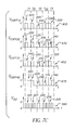
- Fig. 7C shows the row voltage waveform V R2 590 and the four possible column voltage waveforms V Coff12 612 , V Coff22 632 , V Coff32 652, and V Coff42 672 , each having an OFF-state column voltage pulse 240 in the period of T2, but different voltage pulses in the periods of T1 and T2.
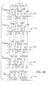
- Fig. 7D shows the resulting pixel voltage waveforms V Poff12 622 , V Poff22 642 , V Poff32 662 , and V Poff42 682 , formed from the row voltage waveform V R2 590 and the four column voltage waveforms V Coff12 612 , V Coff22 632 , V Coff32 652 , and V Coff42 672 , respectively.
- the column voltage pulses 226 in Figs. 7A and 7C take the form of V Coff 240 instead of V Con 220 as in Figs. 6A and 6C, and consequently, the resulting pixel voltage pulses 296 in Figs. 7B and 7D take the form of V Pnsoff 285 instead of V Pnson 265 in Figs. 6B and 6D.
- the inserted framing voltage pulses in the periods of T f1 and T f2 shown in Figs. 7A through 7D take different forms.
- the pixel voltage waveforms V Pon12 522, V Pon22 542, V Pon32 562, and V Pon42 582 have the same RMS values of 1 / 2U , and the same average voltage values ⁇ V> of 1 / 4U .
- the pixel voltage waveforms V Poff12 622, V Poff22 642, V Poff32 662, and V Poff42 682 have the same RMS values of 3 4 U , and the same non-zero local average voltage values ⁇ V> of 1 / 4U .
- FIG. 8A shows the row voltage waveform V R23 593 and the four possible column voltage waveforms, V Con13 513, V Con23 533 , V Con33 553, and V Con43 573, each having an ON-state column voltage pulse 220 in the period of T2, but different voltage pulses in the periods of T1 and T2.
- the corresponding pixel voltage waveforms are V Pon13 523 , V Pon23 543 , V Pon33 563 , and V Pon43 583 , respectively, shown in Fig. 8B.
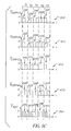
- Fig. 8C shows the row voltage waveform V R23 593 and the four possible column voltage waveforms V Coff13 613, V Coff23 633, V Coff33 653, and V Coff43 673, each having an OFF-state column voltage pulse 240 in the period of T2, but different voltage pulses in the periods of T1 and T2.
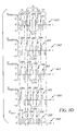
- Fig. 8D shows the resulting pixel voltage waveforms V Poff13 623, V Poff23 643, V Poff33 663, and V Poff43 683, formed from the row voltage waveform V R23 593 and the four column voltage waveforms V Coff13 613 , V Coff23 633 , V Coff33 653 , and V Coff43 673 , respectively.
- the column voltage pulses 225 and 226 in both the first inserted frame T f1 and second inserted frame T f2 in Figs. 8A and 8C take the form of V Coff 240 instead of V Con 220 as in Figs. 6A and 6C.
- the row voltage waveform V R23 593 has a voltage pulse 207 in the first inserted frame T f1 , which is out of phase relative to the voltage pulse 208 in the second inserted frame T f2 .
- the inserted framing voltage pulses in the periods of T f1 and T f2 take different forms on the row voltage waveform. Consequently, the resulting pixel voltage pulses 296 in Figs.
- V Pnsoff 285 instead of V Pnson 265 in Figs. 6B and 6D.
- the resulting pixel voltage pulses 295 in Figs. 8B and 8D have reversed polarity compared to the pixel voltage pulses 295 shown in Figs. 6B, 6D, 7B, and 7D.
- the effective ON-state selection time t on9 associated with the pixel voltage pulse 260 shown in Fig. 8B has the same duration as the effective OFF-state selection time t off9 associated with the pixel voltage pulse 280 as shown in Fig. 8D. Both effective selection times t on9 and t off9 are equal to 1.25T2.
- the pixel voltage waveforms V Pon13 523, V Pon23 543, V Pon33 563, and V Pon43 583 have the same RMS values of 1 / 2U , and the same local average voltage values ⁇ V> of 0 .
- the pixel voltage waveforms V Poff13 623, V Poff23 643, V Poff33 663, and V Poff43 683 have the same RMS values of 3 4 U , and the same local average voltage values ⁇ V> of 0.
- the local average voltage can be varied independent of any data pattern and can be either zero or nonzero. This is a desired property for achieving high display performance.
- Inserting framing voltage pulses according to the invention can be implemented in various ways within the scope of the invention.
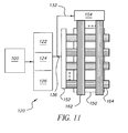
- Fig. 11 shows a display system that can be used to produce the waveforms according to the present invention that includes control electronics 120 and a voltage source 100 that generates a voltage at a maximum voltage U .
- the output voltage U is coupled to a duty cycle controller 122 that generates pulses or voltage signals.
- a phase controller 124 sets the relative phase of a train of row output pulses with respect to the column pulse train, and a frequency controller 126 that sets the period of the output pulses. The period may be the same for both sets of pulses or different.
- the output pulses include column pulses 132 and row pulses 136.
- the display 150 receives the respective pulses in the column driver 154 and the row driver 152 .
- the drivers apply the pulses to the column electrodes and row electrodes 162, 164 of the display.
- the individual controllers 122, 124, and 126 may be separated into two sets of controllers, one set for the rows and one set for the columns.
- Fig. 9A there are shown four curves of reflectance as a function of wavelength for an OFF-state (or dark state) pixel of a cholesteric liquid crystal display, corresponding to four possible data pattern combinations on neighboring pixels: ON-state/ON-state (Curve a), ON-state/Off-state (Curve b), OFF-state/ON-state (Curve c), OFF-state/OFF-state (Curve d), one row before and after the measured OFF-state pixel.
- the reflectance varies from approximately 4.5% to 5.5% (a range of 1%).
- Fig. 9B shows four curves of reflectance as a function of wavelength for an ON-state (or bright state) pixel of a cholesteric liquid crystal display, corresponding to the same four possible data pattern combinations as in Fig. 9A.
- the reflectance varies from approximately 18% to 24% (a range of 6%).
- Figs. 10A and 10B show data analogous to the data shown in Figs. 9A and 9B, obtained with the improved drive scheme of the present invention. Both Figs. 10A and 10B show that the variation of reflectance vs wavelength is reduced substantially compared to the variation shown in Figs. 9A and 9B obtained with a prior art drive scheme.
- the reflectance of the OFF-state at the peak wavelength of 530 nm varies from approximately 4.4% to 4.6% (a range of only 0.2%) as shown in Fig. 10A, and the reflectance of the ON-state at the wavelength of 530 nm changes from about 19% to 22% (a range of 3%).
- the improved drive scheme reduces the data pattern dependent defects for both dark (or OFF-state) and bright (or ON-state) states. It should be noted that the improved drive scheme can also reduce the data pattern dependency of any gray level state.
Landscapes
- Engineering & Computer Science (AREA)
- Chemical & Material Sciences (AREA)
- Crystallography & Structural Chemistry (AREA)
- Physics & Mathematics (AREA)
- Computer Hardware Design (AREA)
- General Physics & Mathematics (AREA)
- Theoretical Computer Science (AREA)
- Control Of Indicators Other Than Cathode Ray Tubes (AREA)
- Liquid Crystal Display Device Control (AREA)
- Liquid Crystal (AREA)
Abstract
Description
- The present invention relates to cholesteric (chiral nematic) liquid crystal displays and their electrical drive schemes, and more particularly to such a drive scheme which eliminates data dependent defects.
- US 5,437,811 issued August 1, 1995 to Doane et al. discloses a light-modulating cell having a chiral nematic liquid crystal (cholesteric liquid crystal) in polymeric domains contained by conventional patterned glass substrates. The chiral nematic liquid crystal has the property of being driven between a planar state reflecting a specific visible wavelength of light and a light scattering focal conic state. Chiral nematic material has two stable states and can maintain one of the stable states in the absence of an electric field.
- US 5,251,048 issued October 5, 1993 to Doane et al., and US 5,644,330 issued July 1, 1997 to Catchpole et al. disclose various driving methods to switch chiral nematic materials between its stable states. However, the update rate of these displays is far too slow for most practical applications. Typically, the update rate was about 10-40 milliseconds per line. It would take a 10-40 seconds to update a 1000 line display.
- US 5,748,277 issued May 5, 1998 to Huang et al., and US 6,154,190 issued November 28, 2000 to Yang et al. disclose fast driving schemes for chiral nematic displays, which are called dynamic drive schemes. The dynamic drive schemes generally comprise a preparation step, a pre-holding step, a selection step, a post-holding step, and an evolution step. These fast driving schemes require very complicated electronic driving circuitry. For example, all column and row drivers must output bi-polar and multiple level voltages. During the image writing, due to a pipeline algorithm used with the drive schemes, there is an undesirable black bar shifting over the frame.
- US 6,268,840 B1 issued July 31, 2001 to Huang, discloses a unipolar waveform drive method to implement the above-mentioned dynamic driving schemes. However, because the amplitude of voltages required in the preparation step, the selection step, and the evolution step are distinct, both column and row drivers are required to generate multilevel unipolar voltages, which is still undesirable.
- Kozachenko et al. (Hysteresis as a Key Factor for the Fast Control of Reflectivity in Cholesteric LCDs, Conference Record of the IDRC 1997, pp. 148-151), Sorokin (Simple Driving Methods for Cholesteric Reflective LCDs, Asia Displays 1998, pp. 749-752), and Rybalochka et al. (Dynamic Drive Scheme for Fast Addressing of Cholesteric Displays, SID 2000, pp. 818-821; Simple Drive scheme for Bistable Cholesteric LCDs,
SID 2001, pp. 882-885) proposed so called U / - Another problem with these drive schemes is data pattern dependent defects. Namely, the effective selection time varies depending on the nonselected pixel voltages preceding and following a selected row, thus the reflective state of a pixel changes in an undesired way. There is a need therefore for an improved dynamic drive scheme that eliminates data pattern dependent defects in a displayed image.
- The need is met according to the present invention by providing a drive scheme for driving the pixels of a passive matrix liquid crystal display having row and column electrodes, the drive scheme including a selection step, the selection step including applying row and column waveforms to the display to generate selected pixel voltage pulses in a selected row and to generate non selected pixel voltage pulses in non selected rows, the selection step having an effective selection time that depends on the preceding and following nonselected pixel voltages, wherein a framing voltage pulse is inserted between each successive selected pixel voltage pulse such that the effective selection time is independent of the preceding and following nonselected pixel voltages, whereby data pattern dependent defects in a displayed image are eliminated.
- The drive scheme of the present invention has the advantage that it produces a uniform display state for each pixel in the display independent of the display state of neighboring pixels. The present invention has the further advantage that it can be applied to a variety of dynamic drive schemes including the U /
- Fig. 1 is a partial perspective view of a prior art cholesteric liquid crystal display;
- Fig. 2A is a schematic diagram of a prior art cholesteric liquid crystal material in a planar state reflecting light;
- Fig. 2B is a schematic diagram of a prior art cholesteric liquid crystal material in a focal conic state forward scattering light;
- Fig. 2C is a schematic diagram of a prior art cholesteric liquid crystal material in a homeotropic state transmitting light;
- Fig. 2D is a plot of the typical response of reflectance of a prior art cholesteric liquid crystal material to a pulsed voltage;
- Fig. 3 is a schematic diagram showing column voltage, row
voltage, and pixel voltage pulses on selected rows in a prior art U /
- Fig. 4 is a schematic diagram showing column voltage, row
voltage, and pixel voltage pulses on non-selected rows in a prior art U /
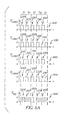
- Fig. 5A is a schematic diagram showing column and row voltage waveforms having an ON-state data on the second row and various combinations of data on the first and third rows by use of waveforms shown in Figs. 3 and 4 (prior art);
- Fig. 5B is a schematic diagram showing data dependency of an effective ON-state selection time by use of waveforms shown in Fig. 5A (prior art);
- Fig. 5C is a schematic diagram showing column and row voltage waveforms having an OFF-state data on the second row and various combinations of data on the first and third rows by use of waveforms shown in Figs. 4A and 4B (prior art);
- Fig. 5D is a schematic diagram showing data dependency of an effective OFF-state selection time by use of waveforms shown in Fig. 5C (prior art);
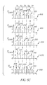
- Fig. 6A is a schematic diagram showing improved row and column voltage waveforms that minimize data dependency of an effective ON-state selection time in accordance with one embodiment of the present invention;
- Fig. 6B is a schematic diagram showing improved pixel voltage waveforms that minimize data dependency of an effective ON-state selection time by use of row and column voltage waveforms shown in Fig. 6A;
- Fig. 6C is a schematic diagram showing improved row and column voltage waveforms that minimize data dependency of an effective OFF-state selection time in accordance with one embodiment of the present invention;
- Fig. 6D is a schematic diagram showing improved pixel voltage waveforms that minimize data dependency of an effective OFF-state selection time by use of row and column voltage waveforms shown in Fig. 6C;
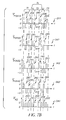
- Fig. 7A is a schematic diagram showing improved row and column voltage waveforms that minimize data dependency of an effective ON-state selection time in accordance with an alternative embodiment of the present invention;
- Fig. 7B is a schematic diagram showing improved pixel voltage waveforms that minimize data dependency of an effective ON-state selection time by use of row and column voltage waveforms shown in Fig. 7A;
- Fig. 7C is a schematic diagram showing improved row and column voltage waveforms that minimize data dependency of an effective OFF-state selection time in accordance with the alternative embodiment of the present invention;
- Fig. 7D is a schematic diagram showing improved pixel voltage waveforms that minimize data dependency of an effective OFF-state selection time by use of row and column voltage waveforms shown in Fig. 7C;
- Fig. 8A is a schematic diagram showing improved row and column voltage waveforms that minimize data dependency of an effective ON-state selection time in accordance with a further alternative embodiment of the present invention;
- Fig. 8B is a schematic diagram showing improved pixel voltage waveforms that minimize data dependency of an effective ON-state selection time by use of row and column voltage waveforms shown in Fig. 8A;
- Fig. 8C is a schematic diagram showing improved row and column voltage waveforms that minimize data dependency of an effective OFF-state selection time in accordance with the further alternative embodiment of the present invention;
- Fig. 8D is a schematic diagram showing improved pixel voltage waveforms that minimize data dependency of an effective OFF-state selection time by use of row and column voltage waveforms shown in Fig. 8C;
- Figs. 9A, 9B are experimental data showing data dependency of an ON-state and an OFF-state, respectively, in a prior art drive scheme using the waveforms shown in Fig. 4A;
- Figs. 10A, 10B are experimental data showing reduced data dependency of an ON-state and an OFF-state, respectively, in drive scheme according to the present invention using the waveforms shown in Fig. 8A;
- Fig. 11 is a schematic block diagram of an LCD display system and the control electronics for performing the invention.
-
- Fig. 1 is partial perspective view of a structure for a
prior art display 10 that can be driven in accordance with the invention.Display 10 includes aflexible substrate 15, which is a thin transparent polymeric material, such as Kodak Estar™ film base formed of polyester plastic that has a thickness of between 20 and 200 microns. Asubstrate 15 can be a 125 micron thick sheet of polyester film base. Other polymers, such as transparent polycarbonate, can also be used. - Electrodes in the form of first
patterned conductors 20 are formed oversubstrate 15. Firstpatterned conductors 20 can be tin-oxide or indium-tin-oxide (ITO), with ITO being the preferred material. Typically, the material of firstpatterned conductors 20 is sputtered as a layer oversubstrate 15 having a resistance of less than 250 ohms per square. The layer is then patterned to form firstpatterned conductors 20 in any well known manner. Alternatively, firstpatterned conductors 20 can be an opaque electrical conductor material such as copper, aluminum, or nickel. If firstpatterned conductors 20 are opaque metal, the metal can be oxidized to create light absorbing firstpatterned conductors 20. Firstpatterned conductors 20 are formed in the conductive layer by conventional photolithographic or laser etching means. - A light modulating material such as a polymer dispersed
cholesteric layer 30 overlays first patternedconductors 20. In a preferred embodiment, the polymer dispersedcholesteric layer 30 includes a polymeric host material and dispersed cholesteric liquid crystal materials, such as those disclosed in US 5,695,682 issued December 9, 1997 to Doane et al., the disclosure of which is incorporated by reference. Application of electrical fields of various amplitude and duration can drive a chiral nematic material into a reflective state, a transmissive state, or an intermediate state. These cholesteric materials have the advantage of maintaining a given state indefinitely after the field is removed. Cholesteric liquid crystal materials can be Merck BL112, BL118 or BL126, available from E.M. Industries of Hawthorne, NY. - The polymeric host material is provided by E.M. Industries cholesteric material BL-118 dispersed in deionized photographic gelatin. The liquid crystal material is dispersed at 8% concentration in a 5% deionized gelatin aqueous solution. The mixture is dispersed to create 10 micron diameter domains of the liquid crystal in aqueous suspension. The material is coated over a patterned ITO polyester sheet to provide a 7 micron thick polymer dispersed cholesteric coating. Other organic binders such as polyvinyl alcohol (PVA) or polyethylene oxide (PEO) can be used. Such compounds are machine coatable on equipment associated with photographic films.
- Electrodes in the form of second
patterned conductors 40 overlay polymer dispersedcholesteric layer 30. Secondpatterned conductors 40 should have sufficient conductivity to establish an electric field across polymer dispersedcholesteric layer 30. Secondpatterned conductors 40 can be formed in a vacuum environment using materials such as aluminum, silver, platinum, carbon, tungsten, molybdenum, tin, or indium or combinations thereof. The secondpatterned conductors 40 are as shown in the form of a deposited layer. Oxides of the metals can be used to darken secondpatterned conductors 40. The metal material can be oxidized by applying energy from resistance heating, cathodic arc, electron beam, sputtering, or magnetron excitation. Tin-oxide or indium-tin-oxide coatings permit secondpatterned conductors 40 to be transparent.Electrodes layer 30 and are in rows and columns, respectively, so that the intersection of a row and column defines pixels for applying an electric field at each intersection across thelayer 30 when a voltage is applied to the electrodes. - Second
patterned conductors 40 are printed conductive ink such as Electrodag 423SS screen printable electrical conductive material from Acheson Corporation. Such printed materials are finely divided graphite particles in a thermoplastic resin. The secondpatterned conductors 40 are formed using the printed inks to reduce display cost. The use of a flexible support forsubstrate 15, laser etching to form firstpatterned conductors 20, machine coating polymer dispersedcholesteric layer 30 and printing secondpatterned conductors 40 permits the fabrication of very low cost memory displays. Small displays formed using these methods can be used as electronically rewritable tags for inexpensive, limited rewrite applications. - Fig. 2A and 2B show two stable states of cholesteric liquid crystals. In Fig. 2A, a high voltage field has been applied and quickly switched to zero potential, which converts cholesteric liquid crystal to a
planar state 22.Incident light 26 with proper wavelength and polarization striking cholesteric liquid crystal inplanar state 22 is reflected as reflected light 28 to create a bright image. In Fig. 2B, application of a lower voltage field leaves cholesteric liquid crystal in a transparent focal conic state 24.Incident light 26 striking a cholesteric liquid crystal in focal conic state 24 is mainly forward scattered. Secondpatterned conductors 40 can be black which absorbs transmitted light 27 to create a dark image when the liquid crystal material is in focal conic state 24. As a result, a viewer perceives a bright or dark image depending if the cholesteric material is inplanar state 22 or focal conic state 24, respectively. The cholesteric liquid crystal material also has a plurality of reflective states when a part of the cholesteric material is inplanar state 22 and the rest is in focal conic state 24. Consequently, a viewer also perceives gray level images. In Fig. 2C, cholesteric liquid crystal is in ahomeotropic state 25 when a high voltage is applied.Incident light 26 illuminating a cholesteric liquid crystal inhomeotropic state 25 is transmitted. - Fig. 2D illustrates the state of the liquid crystal material after the application of various driving voltages thereto. This figure generally corresponds to Fig. 1 of US 5,644,330, referenced above. The liquid crystal material in
layer 30 begins in a first state, either the reflectingplanar state 22 shown in Fig. 2A or the non-reflecting focal conic state 24 shown in Fig. 2B, and is driven with an AC voltage, having an RMS (root mean square) amplitude above V4 in Fig. 2D. When the voltage is removed quickly, the liquid crystal material switches to the reflecting state and will remain reflecting. If driven with an AC voltage between V2 and V3, the material will switch into the non-reflecting state and remain so until the application of a second driving voltage. If no voltage is applied, or the voltage is well below V1, then the material will not change state, regardless of the initial state. - The prior art U /
- For conventional drive schemes as disclosed in US 5,251,048 and 5,644,330, referenced above, the selection time is relatively long, for example 10 to 40 ms and the variation in the pre-selection and post-selection steps do not have much effect on the reflection of the final states. On the contrary, for all high speed drive schemes, the selection time is relatively short, in most cases, less than 1 ms, which is comparable with commonly used period of a voltage waveform (1 ms). Consequently, any variation immediately before and after the selection step has significant impact on the reflection of the final states.
- To better understand the data dependent defects, references are made to Figs. 3 and 4, which are detailed descriptions of the selection step according to the prior art U /
voltage pulse V Rs 200 is applied during a selection time ts. For other non-selected rows, a non-selected rowvoltage pulse V Rns 205 is applied during the selection time ts. Column electrodes receive either a columnvoltage pulse V Con 220 for On-state data or avoltage pulse V Coff 240 for Off-state data. The resulting pixel voltage (the difference between the row voltage and column voltage) on the selected row is eitherV Pson 260 for ON-state orV Psoff 280 for OFF-state. On the non-selected rows, the pixel voltage is eitherV Pnson 265 when the column voltage is VCon orV Pnsoff 285 when the column voltage is VCoff. In this particular example, all row voltage and column voltage pulses (VRs, VRns,VCon,VCoff) take only two levels, either a maximum voltage level U or aminimum voltage level 0. The pixel voltage pulses (VPson, VPsoff, VPnson, VPnoff), however, are bipolar waveforms or zero. The selection time ts is the time duration in the selection step for each selected row. - Referring to Fig. 5A,
V R2 390 is a row voltage waveform applied to the second row. Since the second row is selected to be written in the period of T2, it receives selectedrow voltage pulse 200 in the period of T2, and non-selectedrow voltage pulses 205 in the periods of T1 and T2 when the first row and the third row are selected. Columnvoltage waveforms V Con1 310,V Con2 330,V Con3 350, andV Con4 370 all have the samecolumn voltage pulse 220 corresponding to ON-state data in the period of T2, but four different combinations of column voltage pulses (or data voltage pulses) in the periods of T1 and T2. Thevoltage waveform V Con1 310 has both ON-statedata voltage pulses 220 in the periods of T1 and T3, while thewaveform V Con4 370 has both OFF-statedata voltage pulses 240. On the columnvoltage waveform V Con2 330, an On-statedata voltage pulse 220 appears in the period of T1 and an OFF-statedata voltage pulse 240 in the period of T4. On the contrary, the columnvoltage waveform V Con3 350 has an OFF-statedata voltage pulse 240 in the period of T1 and an ON-statedata voltage pulse 220 in the period of T4. - Fig. 5B is a schematic diagram showing the resulting pixel
voltage waveforms V Pon1 320,V Pon2 340, VPon3 360, andV Pon4 380, formed from the rowvoltage waveform V R2 390, and the four columnvoltage waveforms V Con1 310,V Con2 330,V Con3 350, andV Con4 370, respectively. For the purpose of comparison, the rowvoltage waveform V R2 390 is shown in both Figs. 5A and 5B. All the four pixelvoltage waveforms V Pon1 320,V Pon2 340, VPon3 360, andV Pon4 380 have the same selected ON-statepixel voltage pulse 260 in the selection period of T2 as planned. In this particular example, the selected ON-statepixel voltage pulse 260 is zero volts. However, they have different nonselected voltage pulses, either 265 or 285, immediately before and after the selection period of T2. When the selection period T2 is combined with the period T1 immediately prior to T2, and the period T3 immediately after T2, the ON-statepixel voltage pulses 260 vary their effective ON-state selection times with ton1 onV Pon1 320, ton2 onV Pon2 340, ton3 on VPon3 360, and ton4 onV Pon4 380. The effective ON-state selection times satisfy the relation that ton1=1.5ton4, ton2=ton3=1.25ton4, and ton4=T2. Thus, the maximum effective ON-state selection time ton1 is 50% longer than the minimum effective ON-state selection time ton4, and the other ON-state selection times ton2 and ton3 are both 25% more than ton4. This will result in an undesirable difference in the On-state of the pixel depending on the state of the preceding or following nonselected pixel voltages. - Figs. 5C and 5D are similar to Figs. 5A and 5B, except that an OFF-state data
column voltage pulse 240 is applied in the second period of T2 in the four possible columnvoltage waveforms V Coff1 410,V Coff2 430,V Coff3 450, andV Coff4 370. The resulting pixel voltage waveforms formed from the rowvoltage waveform V R2 390 and the four columnvoltage waveforms V Coff1 410,V Coff2 430,V Coff3 450, andV Coff4 470 areV Poff1 420,V Poff2 440,V Poff3 460, andV Poff4 480, respectively. They all have the same OFF-statepixel voltage pulse 280 in the selection period of T2, but different pixel voltage pulses in the periods immediately before and after T2, either 285 if the column voltage pulse is OFF-state pulse state pulse 220. - When the selection period T2 is combined with the periods T1 and T3 immediately before and after T2, the OFF-state
pixel voltage pulses 280 vary their effective duration with toff1 onV Poff1 420, toff2 onV Poff2 440, toff3 onV Poff3 460, and toff4 onV Poff4 480. The effective OFF-state selection times satisfy that toff4=1.5toff1, toff2=toff3=1.25toff1 and toff1=T2. Thus, the maximum effective OFF-state selection time toff4 is 50% longer than the minimum effective OFF-state selection time toff1, and the other OFF-state selection times toff2 and toff3 are both 25% more than toff1. This will result in an undesirable difference in the Off-state of the pixel depending on the state of the preceding or following nonselected pixel voltages. - Fig. 5B and Fig. 5D clearly show that the effective ON-state and OFF-state selection times depend on the state of neighboring pixels and vary with the data pattern appearing immediately before and after a particular row. The data dependence of the effective selection time causes an unpredictable variation of optical states.
- Although the pixel voltage has an average of zero volts in the selection period of T2, a careful examination of pixel voltage waveforms reveals that the local average voltage <V> over Tc, which is a duration including the selection period T2 and a 50% period before and after T2, also varies with data pattern. Referring back to Fig. 5B, during the period of Tc, which includes the second half of T1, T2, and the first half of T3, the root mean square (RMS) values are 1 / 2 U , but the local average values of voltage <V> are 0, 1 / 4 U, - 1 / 4 U, and 0 on
V Pon1 320,V Pon2 340, VPon3 360, andV Pon4 380 respectively. Referring to Fig. 5D, during the same period of Tc, the pixelvoltage waveforms V Poff1 420,V Poff2 440,V Poff3 460, andV Poff4 480 have the same RMS values of - According to the present invention, the data dependence of the effective selection time is minimized by inserting a framing voltage pulse between each successive selected pixel voltage pulse such that the effective selection time and local average voltage are the same for every pixel in the display, whereby the display state of a pixel is independent of the display state of neighboring pixels.
- A first embodiment of the present invention will be described referring to Figs. 6A through 6D. Fig. 6A shows the row
voltage waveform V voltage waveforms V V V V voltage waveform V R2 390 and four possible columnvoltage waveforms V Con1 310,V Con2 330,V Con3 350, andV Con4 370, shown in Fig. 5A, respectively. - Each of the column
voltage waveforms V V V V framing voltage pulse 225 in the frame period Tf1 inserted prior to the selection period of T2 and another commonframing voltage pulse 226 in the frame period Tf2 inserted after the selection period T2. In the two inserted frame periods of Tf1 and Tf2, the rowvoltage waveform V voltage pulses row voltage pulses 205 in this particular example. - Fig. 6B shows the resulting pixel
voltage waveforms V V V V voltage waveform V V V V V pixel voltage pulses pixel voltage pulses 260 have the same effective ON-state selection time ton7, unchanged in pixelvoltage waveforms V V V V - The same inserted framing voltage pulses also minimizes the data dependence for the effective OFF-state selection time as illustrated in Figs. 6C and 6D. Resulting pixel
voltage waveforms V V V V voltage waveform V V V V V voltage waveforms V V V V column voltage pulse 240 as shown in Fig. 6C, and all pixelvoltage waveforms V V V V pixel voltage pulse 280 as shown in Fig. 6D. Due to the fixedpixel voltage pulses - Referring to Fig. 6B, during the period of Tc, which now includes the second half of Tf1, T2, and the first half of Tf2, the pixel
voltage waveforms V V V V - Referring to Fig. 6D, during the period of Tc, which also includes the second half of Tf1, T2, and the first half of Tf2, the pixel
voltage waveforms V V V V - Although this first embodiment described with respect to Figs. 6A through 6D solves both the problems of variable effective selection time and variable local average selection voltage, the effective ON-state selection time ton7 and OFF-state selection time toff7 are different. This may not be a problem, and may be an advantage in some cases where it is desirable to have different ON-state and OFF-state selection times.
- According to an alternative embodiment of the present invention illustrated in Figs. 7A through 7D, the effective ON-state and OFF-state selection times are made to be the same. Fig. 7A shows the row
voltage waveform V voltage waveforms V V V V column voltage pulse 220 in the period of T2, but different voltage pulses in the periods of T1 and T2. The corresponding pixel voltage waveforms areV V V V - Fig. 7C shows the row
voltage waveform V voltage waveforms V V V V column voltage pulse 240 in the period of T2, but different voltage pulses in the periods of T1 and T2. Fig. 7D shows the resulting pixelvoltage waveforms V V V V voltage waveform V voltage waveforms V V V V - According to this alternative embodiment, in the second inserted frame Tf2, the
column voltage pulses 226 in Figs. 7A and 7C take the form ofV Coff 240 instead ofV Con 220 as in Figs. 6A and 6C, and consequently, the resultingpixel voltage pulses 296 in Figs. 7B and 7D take the form ofV Pnsoff 285 instead ofV Pnson 265 in Figs. 6B and 6D. The inserted framing voltage pulses in the periods of Tf1 and Tf2 shown in Figs. 7A through 7D take different forms. The effective ON-state selection time ton9 associated with thepixel voltage pulse 260 shown in Fig. 7B has the same duration as the effective OFF-state selection time toff9 associated with thepixel voltage pulse 280 as shown in Fig. 7D. Both effective selection times ton9 and toff9 are equal to 1.25T2. This alternative embodiment not only solves both the problems of variable effective selection times and variable local average selection voltage, but also has ton9 and toff9 times that are equal. However, the value of local average selection voltage is not zero. - Referring to Fig. 7B, during the period of Tc, the pixel
voltage waveforms V V V V voltage waveforms V V V V - A still further embodiment of the present invention that has equal ON-state and OFF-state selection times, and that also provides zero value of local average selection voltages is shown in Figs. 8A through 8D. Fig. 8A shows the row
voltage waveform V V V V V column voltage pulse 220 in the period of T2, but different voltage pulses in the periods of T1 and T2. The corresponding pixel voltage waveforms areV V V V - Fig. 8C shows the row
voltage waveform V voltage waveforms V V V V column voltage pulse 240 in the period of T2, but different voltage pulses in the periods of T1 and T2. Fig. 8D shows the resulting pixelvoltage waveforms V V V V voltage waveform V voltage waveforms V V V V - According to this embodiment, the
column voltage pulses V Coff 240 instead ofV Con 220 as in Figs. 6A and 6C. The rowvoltage waveform V voltage pulse 207 in the first inserted frame Tf1, which is out of phase relative to thevoltage pulse 208 in the second inserted frame Tf2. Thus, the inserted framing voltage pulses in the periods of Tf1 and Tf2 take different forms on the row voltage waveform. Consequently, the resultingpixel voltage pulses 296 in Figs. 8B and 8D take the form ofV Pnsoff 285 instead ofV Pnson 265 in Figs. 6B and 6D. In addition, the resultingpixel voltage pulses 295 in Figs. 8B and 8D have reversed polarity compared to thepixel voltage pulses 295 shown in Figs. 6B, 6D, 7B, and 7D. - In return, the effective ON-state selection time ton9 associated with the
pixel voltage pulse 260 shown in Fig. 8B has the same duration as the effective OFF-state selection time toff9 associated with thepixel voltage pulse 280 as shown in Fig. 8D. Both effective selection times ton9 and toff9 are equal to 1.25T2. - Referring to Fig. 8B, during the period of Tc, the pixel
voltage waveforms V V V V - Referring to Fig. 8D, during the period of Tc, the pixel
voltage waveforms V V V V - Thus it can be seen from the above described embodiments that by inserting the frame waveforms according to the present invention control over local average voltage (or DC net voltage) is achieved. The local average voltage can be varied independent of any data pattern and can be either zero or nonzero. This is a desired property for achieving high display performance.
- Inserting framing voltage pulses according to the invention can be implemented in various ways within the scope of the invention. For example, Fig. 11 shows a display system that can be used to produce the waveforms according to the present invention that includes
control electronics 120 and avoltage source 100 that generates a voltage at a maximum voltage U. The output voltage U is coupled to aduty cycle controller 122 that generates pulses or voltage signals. Aphase controller 124 sets the relative phase of a train of row output pulses with respect to the column pulse train, and afrequency controller 126 that sets the period of the output pulses. The period may be the same for both sets of pulses or different. The output pulses includecolumn pulses 132 androw pulses 136. - The
display 150 receives the respective pulses in thecolumn driver 154 and therow driver 152. The drivers apply the pulses to the column electrodes androw electrodes individual controllers - Experimental measurements were taken using cholesteric liquid crystals display driven by a dynamic drive scheme that had the problem that is addressed by the present invention. Referring to Fig. 9A, there are shown four curves of reflectance as a function of wavelength for an OFF-state (or dark state) pixel of a cholesteric liquid crystal display, corresponding to four possible data pattern combinations on neighboring pixels: ON-state/ON-state (Curve a), ON-state/Off-state (Curve b), OFF-state/ON-state (Curve c), OFF-state/OFF-state (Curve d), one row before and after the measured OFF-state pixel. At the
peak wavelength 530 nm, the reflectance varies from approximately 4.5% to 5.5% (a range of 1%). - Fig. 9B shows four curves of reflectance as a function of wavelength for an ON-state (or bright state) pixel of a cholesteric liquid crystal display, corresponding to the same four possible data pattern combinations as in Fig. 9A. At the
peak wavelength 530 nm, the reflectance varies from approximately 18% to 24% (a range of 6%). Although the variations in reflectance value appear small, even small variations, especially in a dark state, result in noticeable defects. - Figs. 10A and 10B show data analogous to the data shown in Figs. 9A and 9B, obtained with the improved drive scheme of the present invention. Both Figs. 10A and 10B show that the variation of reflectance vs wavelength is reduced substantially compared to the variation shown in Figs. 9A and 9B obtained with a prior art drive scheme. For example, the reflectance of the OFF-state at the peak wavelength of 530 nm varies from approximately 4.4% to 4.6% (a range of only 0.2%) as shown in Fig. 10A, and the reflectance of the ON-state at the wavelength of 530 nm changes from about 19% to 22% (a range of 3%). Thus, the improved drive scheme reduces the data pattern dependent defects for both dark (or OFF-state) and bright (or ON-state) states. It should be noted that the improved drive scheme can also reduce the data pattern dependency of any gray level state.
Claims (15)
- An improved drive scheme for driving the pixels of a passive matrix liquid crystal display having row and column electrodes, the drive scheme including a selection step, the selection step including applying row and column waveforms to the display to generate selected pixel voltage pulses in a selected row and to generate non selected pixel voltage pulses in non selected rows, the selection step having an effective selection time that depends on the preceding and following nonselected pixel voltages, wherein the improvement comprises:inserting a framing voltage pulse between each successive selected pixel voltage pulse such that the effective selection time is independent of the preceding and following nonselected pixel voltages, whereby data pattern dependent defects in a displayed image are eliminated.
- The improved drive scheme claimed in claim 1, wherein the display is a cholesteric liquid crystal display and the drive scheme includes a preparation step prior to the selection step and an evolution step following the selection step.
- The improved drive scheme claimed in claim 2, wherein the drive scheme is a three step dynamic drive scheme.
- The improved drive scheme claimed in claim 2, wherein the drive scheme is a four step dynamic drive scheme.
- The improved drive scheme claimed in claim 2, wherein the drive scheme is a five step dynamic drive scheme.
- The improved drive scheme claimed in claim 2, wherein the drive scheme is a unipolar dynamic drive scheme.
- The improved drive scheme claimed in claim 2, wherein the drive scheme is a two voltage level dynamic drive scheme.
- The improved drive scheme claimed in claim 2, wherein the drive scheme is a multi-voltage level dynamic drive scheme.
- The improved drive scheme claimed in claim 1, wherein the display is a reflective display.
- The improved drive scheme claimed in claim 1, wherein the display is a transmissive display.
- The improved drive scheme claimed in claim 1, wherein the drive scheme includes ON-state effective selection time and an OFF-state effective selection time.
- The improved drive scheme claimed in claim 11, wherein the ON-state effective selection time and an OFF-state effective selection time are equal.
- The improved drive scheme claimed in claim 11, wherein the ON-state effective selection time and an OFF-state effective selection time are not equal.
- The improved drive scheme claimed in claim 1, wherein the local average effective selection voltages are independent of the preceding and following nonselected pixel voltages.
- The improved drive scheme claimed in claim 14, wherein the local average effective selection voltages are zero.
Applications Claiming Priority (2)
| Application Number | Priority Date | Filing Date | Title |
|---|---|---|---|
| US352562 | 1994-12-09 | ||
| US10/352,562 US6924783B2 (en) | 2003-01-28 | 2003-01-28 | Drive scheme for cholesteric liquid crystal displays |
Publications (1)
| Publication Number | Publication Date |
|---|---|
| EP1443488A1 true EP1443488A1 (en) | 2004-08-04 |
Family
ID=32655507
Family Applications (1)
| Application Number | Title | Priority Date | Filing Date |
|---|---|---|---|
| EP03079141A Withdrawn EP1443488A1 (en) | 2003-01-28 | 2003-12-19 | Improved drive scheme for cholesteric liquid crystal displays |
Country Status (4)
| Country | Link |
|---|---|
| US (1) | US6924783B2 (en) |
| EP (1) | EP1443488A1 (en) |
| JP (1) | JP4684559B2 (en) |
| CN (1) | CN1517969A (en) |
Families Citing this family (1)
| Publication number | Priority date | Publication date | Assignee | Title |
|---|---|---|---|---|
| WO2006051273A1 (en) * | 2004-11-10 | 2006-05-18 | Magink Display Tecnologies Ltd. | Drive scheme for a cholesteric liquid crystal display device |
Citations (3)
| Publication number | Priority date | Publication date | Assignee | Title |
|---|---|---|---|---|
| US5703615A (en) * | 1992-02-10 | 1997-12-30 | Fuji Photo Film Co., Ltd. | Method for driving matrix type flat panel display device |
| WO1998050804A2 (en) * | 1997-05-07 | 1998-11-12 | Kent State University | Dynamic drive methods and apparatus for a bistable liquid crystal display |
| EP1258860A1 (en) * | 2001-05-09 | 2002-11-20 | Eastman Kodak Company | Drive circuit for cholesteric liquid crystal displays |
Family Cites Families (11)
| Publication number | Priority date | Publication date | Assignee | Title |
|---|---|---|---|---|
| JPS5476095A (en) * | 1977-11-30 | 1979-06-18 | Toshiba Corp | Matrix drive system of storage type liquid crystal element |
| US5695682A (en) | 1991-05-02 | 1997-12-09 | Kent State University | Liquid crystalline light modulating device and material |
| US5251048A (en) | 1992-05-18 | 1993-10-05 | Kent State University | Method and apparatus for electronic switching of a reflective color display |
| DE69229003T2 (en) | 1992-05-18 | 1999-10-21 | Kent State University, Kent | LIQUID CRYSTALINE, LIGHT-MODULATING DEVICE AND MATERIAL |
| US5592190A (en) * | 1993-04-28 | 1997-01-07 | Canon Kabushiki Kaisha | Liquid crystal display apparatus and drive method |
| US5644330A (en) | 1994-08-11 | 1997-07-01 | Kent Displays, Inc. | Driving method for polymer stabilized and polymer free liquid crystal displays |
| US5748277A (en) * | 1995-02-17 | 1998-05-05 | Kent State University | Dynamic drive method and apparatus for a bistable liquid crystal display |
| DE69633429D1 (en) * | 1995-04-25 | 2004-10-28 | Citizen Watch Co Ltd | METHOD AND APPARATUS FOR DRIVING AN ANTIFERROELECTRIC LIQUID CRYSTAL DISPLAY DEVICE |
| US6268840B1 (en) | 1997-05-12 | 2001-07-31 | Kent Displays Incorporated | Unipolar waveform drive method and apparatus for a bistable liquid crystal display |
| JPH11202298A (en) * | 1998-01-16 | 1999-07-30 | Minolta Co Ltd | Riving method for liquid crystal display element |
| JP4706123B2 (en) * | 2000-05-29 | 2011-06-22 | コニカミノルタホールディングス株式会社 | Liquid crystal display device and method for driving liquid crystal display element |
-
2003
- 2003-01-28 US US10/352,562 patent/US6924783B2/en not_active Expired - Fee Related
- 2003-12-19 EP EP03079141A patent/EP1443488A1/en not_active Withdrawn
-
2004
- 2004-01-28 JP JP2004019902A patent/JP4684559B2/en not_active Expired - Fee Related
- 2004-01-29 CN CNA2004100033779A patent/CN1517969A/en active Pending
Patent Citations (3)
| Publication number | Priority date | Publication date | Assignee | Title |
|---|---|---|---|---|
| US5703615A (en) * | 1992-02-10 | 1997-12-30 | Fuji Photo Film Co., Ltd. | Method for driving matrix type flat panel display device |
| WO1998050804A2 (en) * | 1997-05-07 | 1998-11-12 | Kent State University | Dynamic drive methods and apparatus for a bistable liquid crystal display |
| EP1258860A1 (en) * | 2001-05-09 | 2002-11-20 | Eastman Kodak Company | Drive circuit for cholesteric liquid crystal displays |
Non-Patent Citations (1)
| Title |
|---|
| RYBALOCHKA A ET AL: "SIMPLE DRIVE SCHEME FOR BISTABLE CHOLESTERIC LCDS", 2001 SID INTERNATIONAL SYMPOSIUM DIGEST OF TECHNICAL PAPERS. SAN JOSE, CA, JUNE 5 - 7, 2001, SID INTERNATIONAL SYMPOSIUM DIGEST OF TECHNICAL PAPERS, SAN JOSE, CA: SID, US, vol. 32, June 2001 (2001-06-01), pages 882 - 885, XP001054108 * |
Also Published As
| Publication number | Publication date |
|---|---|
| CN1517969A (en) | 2004-08-04 |
| US6924783B2 (en) | 2005-08-02 |
| US20040145549A1 (en) | 2004-07-29 |
| JP2004246354A (en) | 2004-09-02 |
| JP4684559B2 (en) | 2011-05-18 |
Similar Documents
| Publication | Publication Date | Title |
|---|---|---|
| EP1258860B1 (en) | Drive circuit for cholesteric liquid crystal displays | |
| US6816227B2 (en) | Gray scale and color cholesteric liquid crystal displays | |
| US6894668B2 (en) | General 2 voltage levels driving scheme for cholesterical liquid crystal displays | |
| EP0954841B1 (en) | Dynamic drive methods and apparatus for a bistable liquid crystal display | |
| CN1318184A (en) | Fast addressing of bistable liquid crystal displays | |
| KR20000069992A (en) | Apparatus for and method of driving a cholestric liquid crystal flat panel display with initial setting into the nematic state | |
| US7307608B2 (en) | Unipolar drive chip for cholesteric liquid crystal displays | |
| US20130141655A1 (en) | Common Transparent Electrode for Reduced Voltage Displays | |
| US6885357B2 (en) | Method for writing pixels in a cholesteric liquid crystal display | |
| US6710760B1 (en) | Unipolar drive for cholesteric liquid crystal displays | |
| US7432899B2 (en) | Driving scheme for cholesteric liquid crystal display | |
| EP1279159A1 (en) | Driving of display device for obtaining grey scales | |
| JP2006162927A (en) | Cholesteric liquid crystal display device and method for driving cholesteric liquid crystal display element | |
| US6924783B2 (en) | Drive scheme for cholesteric liquid crystal displays | |
| US7432895B2 (en) | Drive for active matrix cholesteric liquid crystal display | |
| WO2010095539A1 (en) | Bistable liquid crystal display panel driving method and driving device |
Legal Events
| Date | Code | Title | Description |
|---|---|---|---|
| PUAI | Public reference made under article 153(3) epc to a published international application that has entered the european phase |
Free format text: ORIGINAL CODE: 0009012 |
|
| AK | Designated contracting states |
Kind code of ref document: A1 Designated state(s): AT BE BG CH CY CZ DE DK EE ES FI FR GB GR HU IE IT LI LU MC NL PT RO SE SI SK TR |
|
| AX | Request for extension of the european patent |
Extension state: AL LT LV MK |
|
| 17P | Request for examination filed |
Effective date: 20041221 |
|
| 17Q | First examination report despatched |
Effective date: 20050120 |
|
| AKX | Designation fees paid |
Designated state(s): DE FR GB NL |
|
| RBV | Designated contracting states (corrected) |
Designated state(s): DE FR GB NL |
|
| 17Q | First examination report despatched |
Effective date: 20050120 |
|
| RAP1 | Party data changed (applicant data changed or rights of an application transferred) |
Owner name: INDUSTRIAL TECHNOLOGY RESEARCH INSTITUTE |
|
| APBK | Appeal reference recorded |
Free format text: ORIGINAL CODE: EPIDOSNREFNE |
|
| APBN | Date of receipt of notice of appeal recorded |
Free format text: ORIGINAL CODE: EPIDOSNNOA2E |
|
| APBR | Date of receipt of statement of grounds of appeal recorded |
Free format text: ORIGINAL CODE: EPIDOSNNOA3E |
|
| APAF | Appeal reference modified |
Free format text: ORIGINAL CODE: EPIDOSCREFNE |
|
| APBT | Appeal procedure closed |
Free format text: ORIGINAL CODE: EPIDOSNNOA9E |
|
| STAA | Information on the status of an ep patent application or granted ep patent |
Free format text: STATUS: THE APPLICATION IS DEEMED TO BE WITHDRAWN |
|
| 18D | Application deemed to be withdrawn |
Effective date: 20140701 |