BACKGROUND OF THE INVENTION
Field of the Invention
The invention relates to an active-drive type pixel
structure comprising at least TFTs (Thin Film Transistors) for
control and drive, and a capacitor for charge retention, and
to an inspection method therefor. More particularly, the
invention relates to an active-drive type pixel structure and
to an inspection method therefor, in which it is possible easily
to inspect, before a pixel is formed, for example, a light emitting
element is deposited, whether the functions of the
above-described TFTs and that of the capacitor for charge
retention are normal or not.
Description of the Related Art
A display using a display panel comprising light emitting
elements arranged in a matrix has been widely developed. Organic
EL (electro-luminescence) element using an organic material for
a light emitting layer has been noticed as a light emitting element
used for such a display panel. The reason is that the element
has had very great practical utility, high efficiency, and a
long life by using, for the light emitting layer of the EL element,
an organic compound by which excellent light emitting
characteristics can be expected.
There has been proposed, as a display panel which uses
the organic EL element, a simple matrix type display panel in
which the EL elements are simply arranged in a matrix and an
active matrix type display panel in which each of the EL elements
arranged in a matrix is provided with active elements comprising
TFT. The latter active matrix type display panel can
advantageously realize less electricity consumption and more
reduced cross talk between pixels in comparison with those of
the former simple matrix type display panel, and, especially,
is suitable for a high-definition display forming a large screen.
FIG. 1 shows a most basic circuit structure for one pixel
10 in a conventional active matrix type display and the structure
has been called as a conductance control method. In FIG. 1,
a gate G of TFT (Tr1) for control, which comprises n-channels,
is connected to a scanning line 1a from a scanning driver 1 and
its source S is connected to a data line 2a from a data driver
2. And, a drain D of the TFT (tr1) for control is connected
to the gate G of TFT (Tr2) for drive, which comprises P-channels,
and also to one terminal of a capacitor C1 for charge retention.
Moreover, a source S of the TFT (Tr2) for drive is connected
to the other terminal of the above-described capacitor C1, and
also to a power supply at the side of an anode (VHanod) which
supplies a driving electric current to an organic EL element
E1 as a light emitting element. Furthermore, a drain D of the
TFT (tr2) for drive is connected to an anode of the above-described
organic EL element E1, and a cathode of the EL element in question
is connected to a power supply at the side of a cathode (VLcath).
The TFT (Tr1) for control passes, from the source to the
drain, an electric current corresponding to a data voltage (V
data) which is supplied from the data line 2a to the source,
when an ON-state control voltage (Select) is supplied to the
gate of the TFT (Tr1) for control in FIG. 1 through the scanning
line 1a. Accordingly, the above-described capacitor C1 is
charged during the ON-state voltage at the gate of the TFT (Tr1)
for control, and the voltage is supplied to the gate of the TFT
(Tr2) for drive. Then, the TFT (Tr2) for drive passes the
electric current based on the gate voltage and the source voltage
to the EL element E1 and the element E1 is driven into light
emitting.
Moreover, though the TFT (Tr1) for control is put into
a so-called CUT-OFF state when the voltage of the gate of the
TFT (Tr1) for control becomes an OFF-state voltage and the drain
of the TFT (Tr1) for control is put into an open state, the gate
voltage of the TFT (Tr2) for drive is maintained by charges
accumulated in the capacitor C1, the driving electric current
is maintained, and light emitting of the EL element E1 is
maintained till the next scanning.
The above-described configuration shows one connection
configuration example of the pixel 10 by the conductance control
method, in which an image is reproduced by arranging a number
of the pixels 10 in the vertical and horizontal directions and
controlling each pixel for turning on or off, based on an image
signal.
Incidentally, defects of TFT and a capacitor in each pixel
cause a defect in pixels in this kind of the active matrix type
displaypanel. Though it is unavoidable in the present situation
to cause some defects in the display panel, the quality of the
display panel is deteriorated to make the panel unsuitable as
a commodity when the number of defects increases.
Therefore, if it is possible easily to inspect the
above-described TFTs and capacity for charge retention for
defects in the state of a semi-processed product before a state
in which the above-described TFTs and capacitor for charge
retention are deposited on a substrate, that is, a state in which
an organic EL element as a light emitting element is formed on
the above-described substrate, it is possible to improve a yield
rate of the display panel. As a result, it is possible to
contribute to the cost reduction. Especially, in comparison
with the case of AM-LCD (active matrix type liquid crystal
display) in which only one TFT is required for each pixel,
inspection for defects in the above-described state of a
semi-processed product becomes more important in AM-OEL (active
matrix type organic EL display) in which equal to or more than
two through four pieces of TFTs are required for each pixel.
On the other hand, since the capacitor for charge retention
is a load of TFT for a pixel (TFT for drive) even in the
above-described state of a semi-processed product, that is, in
the state of the TFT substrate, it is comparatively easy in AM-LCD
to execute inspection for defects even in the state of a TFT
substrate. However, the TFT for drive is in a no-load state
in the case of AM-OEL because the organic EL element is not
deposited on the TFT substrate in the above-described state of
a semi-processed product. Accordingly, it is not easy in such
a state to execute inspection for defects of pixels.
Accordingly, a method, in which a probe is contacted to
a predetermined picture element electrode and the like to measure
impedance for inspection of defects of pixels, has been proposed
in Japanese Patent Publication NO. 2506840 (after the 15th line
in the second column and FIG. 6). Therefore, there is considered
a similar method in which, in order to inspect pixels for defects,
a load is connected to the TFT for drive for example, by contacting
a conductive pin and the like with an electrode on which the
above-described EL element is formed as a light emitting element.
Incidentally, it is unfavorable that there is increased
possibility to cause defects of the light emitting elements,
for example, by deteriorating the above-described electrode when
an operation of contacting the conductive pin and the like with
the electrode on which the above-described EL element is formed
as a light emitting element is executed in a process of inspecting
pixels for defects as described above. Moreover, though it is
considered to use a method in which a load is given to the TFT
for drive in a non-contact state by putting an electrode for
inspection closer to the electrode, on which the light emitting
element is formed, to form a capacitor between both the electrodes,
it is difficult to use the method in an actual manner because
gap adjustment between both the electrodes is extremely delicate.
SUMMARY OF THE INVENTION
The invention has been made to solve the above problems,
and the object of the invention is to provide an active-drive
type pixel structure and an inspection method therefor, by which
defects of the above-described TFTs and capacity for charge
retention can be inspected by use of, for example, a state of
a semi-processed product in which a dummy load for inspection
is deposited on a substrate.
A first aspect of the active-drive type pixel structure
according to the invention which has been made for solving the
above-described problems is a structure which comprises at least:
TFT for control by which control output is generated, based on
potential of a data line; TFT for drive in which a driving electric
current is controlled, based on the control output; and a
capacitor for charge retention in which the control output is
temporarily maintained, and in which one terminal of a dummy
load for inspection is connected to an electric output terminal
of the TFT for drive, and the other terminal of the dummy load
is connected to a line for inspection, as described in claim
1.
And, a second aspect of the active-drive type pixel
structure according to the invention is a structure which
comprises at least: TFT for control by which control output is
generated, based on potential of a data line; TFT for drive in
which a driving electric current is controlled, based on the
control output; and a capacitor for charge retention in which
the control output is temporarily maintained, and in which one
terminal of a dummy load for inspection is connected to an electric
output terminal of TFT for drive, and the other terminal of the
dummy load is connected to a gate of TFT for drive, as described
in claim 2.
Furthermore, a third and a fourth aspects of the
active-drive type pixel structure according to the invention
are a structure which comprises at least: TFT for control by
which control output is generated, based on potential of a data
line; TFT for drive in which a driving electric current is
controlled, based on the control output; and a capacitor for
charge retention in which the control output is temporarily
maintained, and in which one terminal of a dummy load for
inspection is connected to an electric output terminal of TFT
for drive, and the other terminal of the dummy load is connected
to a source or a gate of TFT for control, as described in claim
3.
On the other hand, a first aspect of the inspection method
of an active-drive type pixel structure according to the
invention which has been made for solving the above-described
problems is a method of an active-drive type pixel structure
which comprises at least: TFT for control by which control output
is generated, based on potential of a data line; TFT for drive
in which a driving electric current is controlled, based on the
control output; and a capacitor for charge retention in which
the control output is temporarily maintained, and in which one
terminal of a dummy load for inspection is connected to an electric
output terminal of TFT for drive, and the other terminal of the
dummy load is connected to a line for inspection, and a method
which has: a step in which TFT for control is put into an ON
state; and a step in which a value of an electric current passing
in the dummy load for inspection is measured while changing any
one of a gate voltage, or a source one of TFT for drive, or a
line voltage of a line for inspection or changing two or more
of the voltages in a relative manner to one another, as described
in claim 4.
Moreover, a second aspect of the inspection method of an
active-drive type pixel structure according to the invention
is a method of an active-drive type pixel structure which
comprises at least: TFT for control by which control output is
generated, based on potential of a data line; TFT for drive in
which a driving electric current is controlled, based on the
control output; and a capacitor for charge retention in which
the control output is temporarily maintained, and in which one
terminal of a dummy load for inspection is connected to an electric
output terminal of TFT for drive, and the other terminal of the
dummy load is connected to a gate of TFT for drive, and a method
which has: a step in which TFT for control is put into an ON
state; and a step in which a value of an electric current passing
in the dummy load for inspection is measured while changing either
of a gate voltage, or a source one of TFT for drive, or changing
both of the voltages in a relative manner to each another, as
described in claim 8.
In addition, a third and a fourth aspect of the inspection
method of an active-drive type pixel structure according to the
invention are a method of an active-drive type pixel structure
which comprises at least: TFT for control by which control output
is generated, based on potential of a data line; TFT for drive
in which a driving electric current is controlled, based on the
control output; and a capacitor for charge retention in which
the control output is temporarily maintained, and in which one
terminal of a dummy load for inspection is connected to an electric
output terminal of TFT for drive, and the other terminal of the
dummy load is connected to a source or a gate of TFT for control,
and a method which has: a step in which TFT for control is put
into an ON state; and a step in which a value of an electric
current passing in the dummy load for inspection is measured
while changing any one of the gate voltage or the source one
of TFT for drive, or a voltage at the other terminal of the dummy
load, or changing two or more of the voltages in a relative manner
to one another, as described in claim 12. And, in the inspection
method of an active-drive type pixel structure according to the
invention, the dummy load for inspection is processed to be put
into a high impedance state after a step in which the value of
the electric current passing in the dummy load for inspection
is measured, as described in claim 13.
BRIEF DESCRIPTION OF THE DRAWINGS
FIG. 1 is a connection diagram showing a basic circuit
configuration for one pixel in a conventional active matrix type
display;
FIG. 2 is a connection diagram showing a first embodiment
of the active drive type pixel structure according to the
invention;
FIG. 3 is a characteristic graph showing an operation of
TFT for drive in the configuration shown in FIG. 2;
FIG. 4 is a connection diagram showing a second embodiment
of the active drive type pixel structure according to the
invention;
FIG. 5 is a characteristic view showing an operation of
TFT for drive in the configuration shown in FIG. 4;
FIG. 6 is a connection diagram showing a third embodiment
of the active drive type pixel structure according to the
invention;
FIG. 7 is similarly a connection diagram showing a fourth
embodiment;
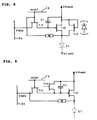
FIG. 8 is a connection diagram showing one example in which
the invention is applied to a pixel with a configuration in which
a reverse bias voltage is effectively applied to an EL element;
FIG. 9 is a connection diagram showing one example in which
the invention is applied to a pixel with a configuration according
to SES method;
FIG. 10 is a connection diagram showing one example in
which the invention is applied to a pixel with a configuration
according to an electric-current programming method;
FIG. 11 is a connection diagram showing one example in
which the invention is applied to a pixel with a configuration
according to a threshold voltage correction method;
FIG. 12 is a connection diagram showing one example in
which the invention is applied to a pixel with a configuration
according to a voltage programming method; and
FIG. 13 is a connection diagram showing one example in
which the invention is applied to a pixel with a configuration
according to a current mirror method.
DESCRIPTION OF THE PREFERRED EMBODIMENTS
Hereinafter, an active drive type pixel structure and an
inspection method therefor according to the invention will be
explained, based on embodiments shown in drawings. Here, in
the following explanation, parts similar to those previously
explained in FIG. 1 are denoted by the same reference numbers
as those in FIG. 1. Therefore, explanation of individual
functions and operations will be suitably eliminated.
In the first place, FIG. 2 shows a first embodiment of
the active drive type pixel structure according to the invention.
The embodiment shown in FIG. 2 shows a similar circuit structure
called as a conductance control method to that of FIG. 1. And,
FIG. 2 shows a state of a semi-processed product of an organic
EL element E1 before a state in which the element E1 is deposited.
The first embodiment shown in FIG. 2 has a configuration
in which one terminal of a dummy load W for inspection is connected
to a drain as an electric current output terminal of TFT (Tr2)
for drive, and the other terminal of the dummy load W is connected
to a line 3 for inspection. That is, the dummy load W for
inspection and the line 3 for inspection are newly provided in
comparison with the configuration of FIG. 1. And, an electric
current measuring means is provided between the line 3 for
inspection and a power supply (VLcath) at the side of a cathode
as described later, and it is inspected by measuring an electric
current value flowing in the dummy load W where the functions
of each TFT (Tr1 and Tr2) and a capacitor C1 for charge retention
are normal or not. That is, a value of an electric current flowing
in the dummy load W is configured to be measured through the
line 3 for inspection in this embodiment.
Here, in the first place, a potential difference of about
15 V is required in order to drive the EL element E1 for light
emitting, considering the potential of each point in the circuit
structure according to the above-described conductance control
method. Then, in order to realize a driving operation at a
voltage which is as low as possible to a reference potential
(ground potential), there is a practical configuration, for
example, in which 10 V is set for a power supply (VHanod) at
the side of an anode of the EL element, and, for example, -5
V is set for a power supply (VLcath) at the side of a cathode
of the EL element.
With regard to a gate voltage of TFT for drive which is
required for ON-OFF control of TFT for drive (Tr2) in the
above-described voltage conditions to be set, a potential of
10 V is required as the lowest one to make TFT be in an OFF state
because TFT for drive is a P channel. Moreover, ON control of
TFT for drive can be realized by applying potential which is
considerably lower than the above-described voltage of 10 V,
for example, ground potential (= 0 V). Thereby, with regard
to a data signal voltage Vdata which is supplied to a source
of TFT (Tr1) for control, VHdata = 10 V is set as high-level
potential, and VLdata = 0 V is done as low-level potential,
respectively, according to the above-described conditions.
On the other hand, a control (selectable) voltage of 12
V which is obtained by adding at least a threshold voltage of
2 V to VHdata = 10 V is required to be supplied to the gate of
TFT (Tr1) in order to supply the above-described VHdata or VLdata
in a selective manner to the gate of TFT (Tr2) for drive. And,
TFT (Tr1) for control concerned can be in a cut off state at
non-scanning by applying, for example, ground potential (= 0
V) to the gate of TFT (Tr1) for control.
In the f irst place, potential bywhich TFT (Tr1) for control
can be in an ON state, that is, the above-described voltage of
12 V is applied to a scanning line 1a in order to inspect a pixel
function in the embodiment shown in FIG. 2, based on the
above-description consideration. When the potential of a data
line 2a is gradually decreased (swept) from 10 V (=VHanod) under
such conditions, the state of TFT (Tr2) for control is gradually
changed to ON. Here, FIG. 3 shows a process in which the state
of TFT for drive is gradually changed to ON.
That is, the horizontal axis shown in FIG. 3 indicates
voltages applied to the data line 2a (source of TFT for control)
and the potential shown as Vdata is decreased from 10 V in the
left direction. And, the vertical axis shown in FIG. 3 indicates
an electric current value Id which passes in the power supply
(VLcath) at the side of the cathode from the drain of TFT (Tr2)
for drive through the dummy load W and the line 3 for inspection.
Accordingly, a characteristic shown in FIG. 3 is approximately
equal to an Id-Vgs characteristic of TFT (Tr2) for drive (voltage
characteristic between a drain electric current and a voltage
between the gate and the source).
Here, the above-described electric current Id passing
through the line 3 for inspection can be obtained by the electric
current measuring means provided between the line 3 for
inspection and the power supply (VLcath) at the side of the cathode,
though not specifically shown in the drawings. Accordingly,
when the electric current passes on the line 3 for inspection,
or conversely when the electric current keeps passing on the
line 3 for inspection regardless of the value of the data line
voltage (Vdata), it is judged that any one of the above-described
TFTs (Tr1 and Tr2) and the capacitor C1 is defective. And, it
is decided that TFT (Tr2) for drive is defective if a Vgs value
(= Vth: threshold voltage), at which an electric current Id with
a predetermined value passes, exceeds a specified voltage.
A panel is judged to be a non-defective article if each
pixel is evaluated and a number of defective pixels in the panel
is with in a specified number, and the panel is judged to be
defective goods if the number of defective pixels exceeds the
specified number. When the inspection is completed as described
above, the dummy loadW connected to each TFT for drive is processed
so that the load W is put into a high impedance state. That
is, the dummy load is processed to be idle by execution of the
above-described processing because an electrically
short-circuit state is caused by the above-described dummy load
Wwhen an EL element is deposited to form a light-emitting display
panel.
As one example in which the above-described dummy load
W is processed to be put into a high impedance state, the dummy
load for inspection is considered to be destroyed (burned off)
by a laser beam. Thereby, electric connection between the drain
of each TFT for drive and the line 3 for inspection is terminated.
Moreover, means by which a dummy load for inspection is fused
by passing a predetermined electric current in a dummy load W
for inspection is preferably adopted, though explanation will
be given in detail in the after-described embodiment. On the
other hand, the above-described dummy load W for inspection may
be an element, TFT, or an element such as a diode, which have
the same function as that of a so-called fuse which is fused
when an electric current equal to or larger than a predetermined
current passes, other than a simple wire and a simple resistance.
Here, the current Id passing in the dummy load W, that
is, the electric current Id passing on the line 3 for inspection
is configured to be measured by changing the potential Vdata
of the data line 2a, in other words, by changing the gate voltage
of TFT (Tr2) for drive in the above explained inspection method
of the first embodiment. However, an I-V (electric
current-voltage) characteristic, as shown in FIG. 3, of TFT for
drive can be obtained even by changing a line voltage (VLcath)
applied to the line 3 for inspection or a driving voltage (VHanod)
supplied to the source of TFT for drive (Tr2) in a separate manner,
or by changing two or more of the above-described voltages in
a relative manner to one another. Thereby, it can be inspected
in the same manner as the above-described case whether the
function of TFTs (Tr1 and Tr2), or the capacitor C1 of each pixel
is normal or not.
Subsequently, FIG. 4 shows a second embodiment of the
active drive type pixel structure according to the invention.
The embodiment shown in FIG. 4 shows a similar circuit structure
called as a conductance control method to that of FIG. 1. In
the same manner as that of the first embodiment, FIG. 4 shows
a state of a semi-processed product of an organic EL element
E1 before a state in which the element E1 is deposited. In the
second embodiment, one terminal of a dummy load W for inspection
is connected to a drain as an electric current output terminal
of TFT (Tr2) for drive, and the other terminal of the dummy load
W is connected to a gate of TFT (Tr2) for drive.
And, an electric current measuring means is configured
to be provided between a data line 2a and a not-shown power supply
(equivalent to the data driver 2 in FIG. 1) which supplies a
data line voltage (Vdata) to the data line 2a and to measure
a value of an electric current passing on the data line 2a. The
data line electric current in this case is obtained after a drain
electric current Id of TFT (Tr2) for drive passes through the
dummy load W and TFT (Tr1) for control. Accordingly, the
above-described data line electric current is approximately
corresponding to the drain electric current Id of TFT (Tr2) for
drive.
In the same manner as that of the first embodiment shown
in FIG. 2, a voltage by which TFT (Tr1) for control can be in
an ON state, for example, 12 V is applied to a scanning line
1a in order to inspect a pixel in a pixel configuration shown
in FIG. 4. Under such a condition, the voltage of data line
2a is sequentially changed to V1, V2 and V3. That is, each value
of the above-described V1, V2, and V3 are changed so that the
voltage levels are changed in dropping order within a range below
the level of 10V (= VHanod) at which TFT (Tr2) for drive is put
into a cut-off state. FIG. 5 shows a changing state of the data
line electric current (drain electric current Id of TFT for drive)
at this time. Here, the characteristics are similar to those
of FIG. 3 which have already been explained.
As shown in FIG. 5, a value of an electric current value
Id1 when V1 is supplied as a voltage of the data line 2a and
a value of an electric current value Id2 when V2 is supplied
as a voltage of the data line 2a are measured, and, when the
electric current values Idl, Id2 are within the specified ranges,
respectively, it is judged that the functions of TFT (Tr1 and
Tr2) and capacitor C1 are normal. Here, an element with a similar
function to that of a so-called fuse which is fused when an electric
current equal to or larger than a predetermined electric current
Idx passes is adopted as the above-described dummy load W in
this embodiment in this embodiment.
Then, V3 is supplied to the data line 2a, as shown in FIG.
5. Potential shown as V3 is supplied as gate bias of the TFT
(Tr2) for drive and a drain electric current at this time is
set so that an electric current equal to or larger than the
above-described Idx passes. Accordingly, the above-described
dummy load W is fused by the drain electric current of TFT for
drive. At this time, it is confirmed through the data line 2a
whether the above-described drain electric current Id is
approximately zero or not. That is, the quality of each pixel
is judged according to the above-described process. Then, the
quality of each panel is judged in the same manner as that of
the embodiment which has been explained, referring to FIG. 2
and FIG. 3.
Here, in the inspection method according to the
above-described second embodiment, the electric current Id
passing in the dummy load W is configured to be measured on the
data line 2a by changing the potential Vdata of the data line
2a, in other words, by changing the gate voltage of TFT (Tr2)
for drive. However, an I-V (electric current-voltage)
characteristic, as shown in FIG. 5, of TFT for drive can be obtained
even by changing the driving voltage (VHanod) supplied to the
source of TFT (Tr2) for drive, or by changing both of the above
potential Vdata of the above-described data line 2a and the
driving voltage VHanod in a relative manner to each other.
Thereby, it can be inspected even by such means, in the same
manner as that of the first embodiment, whether the function
of TFTs (Tr1 and Tr2), or the capacitor C1 of each pixel is normal
or not.
FIG. 6 shows a third embodiment of an active-drive type
pixel structure according to the invention. The embodiment
shown in FIG. 6 shows a similar circuit structure called as a
conductance control method to that of FIG. 1. In the same manner
as that of the first embodiment, FIG. 6 shows a state of a
semi-processed product of an organic EL element E1 before a state
in which the element E1 is deposited. In the third embodiment,
one terminal of a dummy load W for inspection is connected to
a drain as an electric current output terminal of TFT (Tr2) for
drive, and the other terminal of the dummy load W is connected
to a source of TFT (Tr1) for drive.
Even in this example, in the same manner as that of the
example shown in FIG. 4, an electric current measuring means
is configured to be provided between a data line 2a and a not-shown
power supply which supplies a data line voltage Vdata to the
data line 2a, and to measure a value of an electric current passing
on the data line 2a. That is, the value of the electric current
passing on the data line 2a is corresponding to the drain electric
current Id of TFT (Tr2) for drive in the same manner as that
of the example shown in FIG. 4, and it can be inspected by checking
a relation between the data voltage V data and the drain electric
current Id whether the function of TFTs (Tr1 and Tr2), or the
capacitor C1 of each pixel is normal or not.
Then, the dummy load W for inspection is configured to
be fused by destroying (burning off) the load with a laser beam
or by passing a predetermined electric current in the load W
when the above-described measurement is completed. Even in this
embodiment shown in FIG. 6, an I-V (electric current-voltage)
characteristic of TFT for drive can be obtained by changing a
driving voltage (VHanod). Accordingly, in a similar manner to
the above-described case, it can be inspected even by adopting
such means whether the function of TFTs (Tr1 and Tr2), or the
capacitor C1 of each pixel is normal or not.
Here, the drain electric current Id of TFT for drive can
be substantially obtained on the data line 2a not through TFT
(Tr1) for control according to the embodiment shown in FIG. 6,
different from the embodiment shown in FIG. 4. Therefore, an
advantage that TFT with remarkably high current-carrying
capacity is not required to be formed as TFT (Tr1) for control
can be obtained according to the embodiment shown in this FIG.
6.
FIG. 7 shows a fourth embodiment of an active-drive type
pixel structure according to the invention. The embodiment
shown in FIG. 7 shows a similar circuit structure called as a
conductance control method to that of FIG. 1. In the same manner
as that of the first embodiment, FIG. 7 shows a state of a
semi-processed product of an organic EL element E1 before a state
in which the element E1 is deposited. In the fourth embodiment,
one terminal of a dummy load W for inspection is connected to
a drain as an electric current output terminal of TFT (Tr2) for
drive, and the other terminal of the dummy load W is connected
to a source of TFT (Tr1) for drive.
In this example, a not-shown electric current measuring
means is configured to be provided between a scanning line 1a
and a not-shown power supply (equivalent to the scanning driver
1 in FIG. 1) which supplies a control (selectable) voltage to
the scanning line 1a and to measure a value of an electric current
passing on the scanning line 1a. In this case, the electric
current passing on the scanning line 1a is obtained after a drain
electric current Id of TFT (Tr2) for drive passes through the
dummy load W. Accordingly, the above-described electric
current on the scanning line 1a is approximately corresponding
to the drain electric current Id of TFT (Tr2) for drive.
Here, a value of an electric current (substantially, the
drain electric current Id of TFT for drive), which is
corresponding to a data voltage Vdata to be added to a data line
2a and passes on the scanning line 1a, is configured to bemeasured.
Thereby, it can be inspected by checking a relation between the
data voltage V data and the drain electric current Id whether
the function of TFTs (Tr1 and Tr2), or a capacitor C1 of each
pixel is normal or not.
In this case, the drain electric current Id of TFT for
drive cannot be detected on the scanning line 1a due to potential
difference when a voltage by which TFT (Tr1) for control is put
into a ON state, for example, the above-described voltage of
12 V is constantly applied to the scanning line 1a. Then, an
ON voltage supplied to the gate of TFT (Tr1) for control through
the scanning line 1a is required to be controlled in a variable
manner corresponding to the data voltage Vdata supplied to the
data line 2a.
Then, the dummy load W for inspection is configured to
be fused by destroying (burning off) the load W with a laser
beam or by passing a predetermined electric current in the load
W when the above-described measurement is completed. Even in
this embodiment shown in FIG. 7, an I-V (electric
current-voltage) characteristic of TFT for drive can be obtained
by changing a driving voltage (VHanod). Accordingly, in a
similar manner to the above-described case, it can be inspected
even by adopting such means whether the function of TFTs (Tr1
and Tr2), or the capacitor C1 of each pixel is normal or not.
Here, the drain electric current Id of TFT for drive can
be substantially obtained on the data line 2a not through TFT
(Tr1) for control according to the embodiment shown in FIG. 7,
different from the embodiment shown in FIG. 4. Therefore, an
advantage that TFT with remarkably high current-carrying
capacity is not required to be formed as TFT (Tr1) for control
can be obtained even according to the embodiment shown in this
FIG. 7.
Subsequently, there is shown in FIG. 8 a configuration
which is the same as the configuration shown in FIG. 7, though
a diode element is further parallel-connected between the source
and the drain of TFT (Tr2) for drive. That is, this invention
is adopted as one example to a configuration in which a reverse
bias voltage is configured to be applied in an effective manner
to an EL element E1 by parallel connection of the diode element
as described above. Here, TFT (Tr3) is used as the diode element
in the example shown in FIG. 8 to form a diode element in an
equivalent manner by short-circuit between the gate and the
source of TFT (Tr3).
The diode element is arranged as described above, and the
reverse bias voltage is effectively applied to the EL element
E1 through the above-described diode element, for example, by
exchanging VHanod and VLcath as the driving voltage source at
predetermined timing. Thereby, the lifetime of the EL element
can be extended. Here, means for applying a reverse bias voltage
as shown in FIG. 8 has been filed as Japanese Patent Application
No. 2002-230072 by the applicant of this invention. Accordingly,
a similar advantage to that of the configuration example shown
in FIG. 7 can be obtained even in the configuration shown in
FIG. 8.
FIG. 9 shows an example in which the invention is applied
to a pixel configuration which comprises three TFT methods to
realize digital gradation. A driving method for the
configuration is also called as SES (Simultaneous-Erasing-Scan)
and comprises TFT (Tr4) for erase in addition to TFT (Tr1) for
control and TFT (Tr2) for drive. TFT (Tr4) for erase can
discharge electric charge by ON operation of the TFT (Tr4) in
the middle of the lighting period of an EL element E1. Thereby,
gradation driving can be realized to control the lighting period
of the EL element E1.
Even in the configuration shown in FIG. 9, one terminal
of a dummy load W for inspection is connected to a drain as the
electric current output terminal of TFT (Tr2) for drive, and
the other terminal of the dummy load W is connected to a source
of TFT (Tr1) for drive in the same manner as that of the example
shown in FIG. 6. Accordingly, a similar advantage to the one
explained based on FIG. 6 can be obtained even in the configuration
shown in FIG. 9.
FIG. 10 shows an example in which the invention is applied
to a pixel configuration according to an electric-current
programming method. The electric-current programming method
has a configuration in which TFT (Tr5) for switching is connected
to a drain of TFT (Tr2) for drive, and an EL element E1 is formed
at a drain of TFT (Tr5) for switching. And, a capacitor C1 for
charge retention is connected between the source and the gate
of the TFT (Tr2) for drive, and TFT (Tr1) for control is connected
between the gate and the drain of TFT (Tr2) for drive.
Furthermore, an electric current source Is for write is
connected to the source of TFT (Tr1) for control. Additionally,
each gate of TFT (Tr1) for control and TFT (Tr5) for switching
is connected to a scanning line 1a. The above-described electric
current source Is for write has a function to control an electric
current on a data line 2a.
In the configuration shown in FIG. 10, one terminal of
a dummy load W for inspection is connected to the drain of TFT
(Tr5) for switching, and the other terminal of the dummy load
W is connected to the gate of TFT (Tr1) for control. Therefore,
a drain electric current Id of TFT (Tr2) for drive passes in
the dummy load W through TFT (Tr5) for switching, and the drain
electric current Id can be measured on the scanning line 1a
according to this configuration. Thereby, a similar advantage
to the one explained based on FIG. 7 can be obtained even in
the configuration shown in FIG. 10.
Then, assuming that a configuration in FIG. 11 is based
on a method called as a threshold voltage correction method,
FIG. 11 shows an example in which the invention is applied to
a pixel configuration according to a threshold voltage correction
method. The threshold voltage correction method shown in FIG.
11 has similar basic components to those of the conductance
control method shown in FIG. 7. But, a circuit in which a diode
element D1 is parallel-connected between the source and the drain
of TFT (Tr6) is inserted between TFT (Tr1) for control and TFT
(Tr2) for drive in comparison with the configuration of the
conductance control method. Here, the above-described TFT
(Tr6) has a configuration in which the gate and the drain are
in a short-circuit state to realize a function as an element
supplying a threshold characteristic from TFT (Tr1) for control
to the gate of TFT (Tr2) for drive.
According to the configuration, the threshold
characteristic of TFT (Tr2) for drive can be effectively
cancelled by the threshold characteristic generated by TFT (Tr6).
Even in this embodiment, one terminal of a dummy load W for
inspection is connected to the drain of TFT (Tr2) for drive,
and the other terminal of the dummy load W is connected to the
gate of TFT (Tr1) for control.
Therefore, a drain electric current Id of TFT (Tr2) for
drive can be measured on a scanning line 1a even in the
configuration shown in FIG. 11. Thereby, a similar advantage
to the one explained based on FIG. 7 can be obtained even in
the configuration shown in FIG. 11.
FIG. 12 shows an example in which the invention is applied
to a pixel configuration according to a voltage programming
method. In the voltage programming method, TFT (Tr7) for
switching is connected to a drain of TFT (Tr2) for drive, and,
furthermore, TFT (Tr8) for switching is connected between a drain
and a gate of TFT (Tr2) for drive.
Additionally, the voltage programming method has a
configuration in which a data signal is supplied from a data
line 2a to the gate of TFT (Tr2) for drive through TFT (Tr1)
and a capacitor C2.
In the above-described voltage programming method, TFT
(Tr7) and TFT (Tr8) are put into an ON state to secure an ON
state of TFT (Tr2) for drive. TFT (Tr7) is put into an OFF state
at the next moment to sneak a drain electric current Id of TFT
(Tr2) for drive into the gate of TFT (Tr2) for drive through
TFT (Tr8). Thereby, a voltage between the gate and the sources
is increased until the voltage between the gate and the source
of TFT (Tr2) for drive becomes equal to the threshold voltage
of TFT for drive. TFT (Tr2) for drive is put into an OFF state
when both the voltages become equal.
Then, the voltage between the gate and the source is
maintained in a capacitor C1 by which the drain electric current
of TFT for drive is controlled. That is, the voltage programming
method has a configuration in which the scatter in the threshold
voltages in TFT (Tr2) for drive is compensated.
In the above-described configuration shown in FIG. 12,
one terminal of a dummy load W for inspection is connected to
the drain of TFT (Tr7) for drive, and the other terminal of the
dummy load W is connected to the source of TFT (Tr1) for control.
Accordingly, the drain electric current Id of TFT (Tr2) for drive
can be detected on the data line 2a through TFT (Tr2) and the
dummy load W. Therefore, a similar advantage to the one explained
based on FIG. 6 can be obtained even in the configuration shown
in FIG. 12.
FIG. 13 shows an example in which the invention is applied
to a pixel configuration according to a current mirror method.
In the current mirror method, TFT (Tr2) for control, which
comprises P channels, and TFT (Tr9), which also comprises P
channels, are symmetrically provided under common gate
connection, and a capacitor C1 for charge retention is connected
between the gates and the sources of both of TFTs (Tr2 and Tr9).
Moreover, TFT (Tr1) for control is connected between the
gate and the drain of the above-described TFT (Tr9), and TFTs
(Tr2 and Tr9) function as a current mirror by ON operation of
TFT (Tr1) for control. That is, ON operation of TFT (Tr10) for
switching, which comprises N channels, is configured to be
executed together with ON operation of TFT (Tr1) for control.
Thereby, an electric current source Is for write is configured
to be connected to TFT (Tr9) through TFT (TR10) for switching.
Then, an electric current path along which an electric
current passes from the power supply VHanod to the electric
current source Is for write through TFT (Tr9) and TFT (Tr10)
is formed during an address period. And an electric current
corresponding to the electric current passing in the electric
current source Is is generated as the drain electric current
Id of TFT (Tr2) for drive by the current mirror operation.
The gate voltage of TFT (Tr9), which corresponds to the
value of the electric current passing in the electric current
source Is for write, is written into the capacitor C1 by such
an operation. And, TFT (Tr1) for control is put into an OFF
state after a predetermined value of a voltage is written in
the capacitor C1, and TFT (Tr2) for drive operates so that a
predetermined drain electric current Id is supplied, based on
charges accumulated in the capacitor C1.
Moreover, in the embodiment shown in FIG. 13, one terminal
of a dummy load W for inspection is connected to the drain as
the electric output terminal of TFT (Tr2) for drive, and the
other terminal of the dummy load W is connected to the source
of TFT (Tr1) for control. Accordingly, the drain electric
current Id of TFT (Tr2) for drive can be measured on a scanning
line 1a even in the configuration shown in FIG. 13. Therefore,
a similar advantage to the one explained based on FIG. 7 can
be obtained even in the configuration shown in FIG. 13.