TECHNICAL FIELD
The present invention relates to a heat-resistant
optical device which, even when heat is applied, is
stable in various properties.
BACKGROUND ART
Optical devices, such as phase difference films and
circularly polarized light controlling optical devices,
are used, for example, in image display devices. In use,
the optical device is in some cases incorporated in
image display devices such as liquid crystal display
devices. In the production of these image display
devices, the assembly is sometimes heated at 200°C or
above, for example, for the formation of a polyimide
film used as an aligning film or for the formation of an
ITO film as a transparent electrode. Further, when the
image display device using the optical device is used as
a display in the inside of a car, the image display
device is exposed to sunlight and consequently is
sometimes heated by the sunlight to 100°C or above.
Therefore, the optical device, such as the phase
difference film, used in image display devices such as
liquid crystal display devices is possibly heated to a
temperature of 100°C or above and in some cases to 200°C
or above, depending upon the order of the incorporation
of the optical device or the place where the Optical
device is used.
On the other hand, in recent years, as described,
for example, in Japanese Patent Laid-Open No.
100045/2001 and Published Japanese Translation of PCT
Publication No. 508882/1998, Optical devices produced by
polymerizing a polymerizable liquid crystal material
have been proposed. These optical devices are
advantageous in that properties of a liquid crystal can
be anchored or immobilized by polymerization and can be
used as a film. This has led to expectation of the
development of optical devices to various applications.
Regarding optical devices such as phase difference
films, Japanese Patent Laid-Open No. 2109/1993 discloses
a stretched phase difference film possessing excellent
heat resistance. Japanese Patent Laid-Open No.
142510/1993 discloses an optical device comprising a
thermally polymerizable liquid crystalline polymer
possessing excellent heat resistance. Further, Japanese
Patent Laid-Open No. 133628/2001 discloses a highly
heat-resistant polarizing diffractive film comprising a
liquid crystal material which contains a polymeric
liquid crystal and a crosslinkable material.
The optical device produced by polymerizing the
polymerizable liquid crystal material, however, suffers
from a problem that, for example, in the case of a
cholesteric layer having cholesteric regularity, upon
heating, a shift in center reflection wavelength
disadvantageously occurs. Therefore, as described above,
in use, when the optical device is incorporated in an
image display device such as a liquid crystal display
device, disadvantageously, the optical device can be
used only in a site not exposed to heat during the
production of the image display device.
Further, the stretched phase difference film
disadvantageously undergoes a change in phase difference
level at 80°C or above, particularly at 100°C or above,
and, thus, when used, for example, in on-vehicle LCDs,
poses an uneven display or other problems.
DISCLOSURE OF THE INVENTION
In view of the above problems of the prior art, the
present invention has been made, and a main object of
the present invention is to provide an optical device in
which a polymerizable liquid crystal material various
optical characteristics of which is stable even against
heating during manufacture of an optical apparatus such
as an image display device is cured.
The above object can be attained by an optical
device characterized by comprising a support and an
optical function layer provided on the support and
formed by curing a polymerizable liquid crystal material
while retaining predetermined liquid crystal regularity,
the optical device having been heat treated at a
predetermined temperature, said optical function layer
having a percentage reduction in layer thickness,
defined by (A - B)/A, of not more than 5% wherein A
represents the thickness of the optical function layer
after the heat treatment and B represents the thickness
of the optical function layer after reheating the
optical device at said heat treatment temperature for 60
min. When the percentage reduction in layer thickness
upon heating for 60 min at the same temperature as the
heat treatment temperature is within the above defined
range, for example, the change in retardation value in
the case of the use of the optical device as a phase
difference plate and the change in center reflection
wavelength in the case of the use of the optical device
as a circularly polarized light controlling optical
device can be minimized. Therefore, even when the
optical device is incorporated in various image display
devices, the change in function of the optical device
can be minimized.
In a preferred embodiment of the present invention,
the polymerizable liquid crystal material contains a
photopolymerization initiator. This is because, when the
polymerizable liquid crystal material is cured, for
example, by ultraviolet light, the incorporation of a
photopolymerization initiator is preferred from the
viewpoint of accelerating polymerization. Further, an
optical function layer formed by curing a polymerizable
liquid crystal material containing a photopolymerization
initiator can effectively develop the advantage of the
present invention.
More preferably, the support is a supporting
substrate having an aligning ability. This is
advantageous from the viewpoint of the process, because,
when an optical function layer can be formed on a
supporting substrate having an aligning ability and as
such can be used, there is no need to perform the step
of transfer and the like.
According to another aspect of the present
invention, there is provided a retardation layer
laminate characterized by comprising a support and a
retardation layer provided on the support and formed by
curing a polymerizable liquid crystal material while
retaining nematic regularity, smectic regularity, or
cholesteric regularity, said retardation layer laminate
having been heat treated at a predetermined temperature,
said retardation layer having a percentage reduction in
retardation, defined by (Ra - Rb)/Ra, of not more than
5% wherein Ra represents the retardation value of the
retardation layer after the heat treatment and Rb
represents the retardation value of the retardation
layer after reheating the retardation layer laminate at
said heat treatment temperature for 60 min. When the
retardation layer laminate is incorporated in various
image display devices, a change in retardation value
upon heating within the above range poses no problem
associated with the use of the retardation layer
laminate.
In a preferred embodiment of the present invention,
the polymerizable liquid crystal material comprises a
photopolymerization initiator and a polymerizable liquid
crystal monomer. More preferably, the polymerizable
liquid crystal material having cholesteric regularity
comprises a photopolymerization initiator, a
polymerizable liquid crystal monomer, and a
polymerizable chiral dopant. The retardation value is a
value associated with the thickness of the retardation
layer. The change in thickness of the retardation layer
upon heating is estimated to depend upon the amount of
the residue of the photopolymerization initiator.
Therefore, when, the polymerizable liquid crystal
material contains a photopolymerization initiator, it is
considered that the advantage of the present invention
can be utilized.
More preferably, the support is a supporting
substrate having an aligning ability. This is
advantageous from the viewpoint of the process, because,
when a retardation layer can be formed on a supporting
substrate having an aligning ability and as such can be
used as a retardation layer laminate, there is no need
to perform the step of transfer and the like.
According to still another aspect of the present
invention, there is provided a circularly polarized
light controlling optical device characterized by
comprising a support and a cholesteric layer provided on
the support and formed by curing a polymerizable liquid
crystal material while retaining cholesteric regularity,
said circularly polarized light controlling optical
device having been heat treated at a predetermined
temperature, said cholesteric layer having a percentage
change in center reflection wavelength, defined by |λa -
λb|/λa, of not more than 5% wherein λa represents the
center reflection wavelength of the cholesteric layer
after the heat treatment and λb represents the center
reflection wavelength of the cholesteric layer after
reheating the circularly polarized light controlling
optical device at said heat treatment temperature for 60
min. For example, when the circularly polarized light
controlling optical device is incorporated in an image
display device such as a color filter, a change in
center reflection wavelength upon heating within the
above range poses no problem associated with the use of
the circularly polarized light controlling optical
device.
In a preferred embodiment of the present invention,
the polymerizable liquid crystal material comprises a
photopolymerization initiator, a polymerizable liquid
crystal monomer, and a polymerizable chiral dopant. The
center reflection wavelength of the cholesteric layer
depends upon the helical pitch, and a change in layer
thickness causes a change in helical pitch. Accordingly,
for the same reason as described above, the
polymerizable liquid crystal material preferably
contains a photopolymerization initiator.
More preferably, the -support is a supporting
substrate having an aligning ability. This is
advantageous from the viewpoint of the process, because,
when a cholesteric layer can be formed on a supporting
substrate having an aligning ability and as such can be
used as the circularly polarized light controlling
optical device, there is no need to perform the step of
transfer and the like.
According to a further aspect of the present
invention, there is provided a method for heat treating
an optical device, characterized by comprising the step
of heat treating, at a predetermined temperature, an
optical device comprising a support and an optical
function layer provided on the support and formed by
curing a polymerizable liquid crystal material while
retaining predetermined liquid crystal regularity,
whereby heat resistance is imparted to the optical
device. The heat treatment in the above temperature
range can previously remove ingredients which are
removed at the time of heating of the inside of the
optical function layer. Further, the degree of
polymerization of the polymerizable liquid crystal
material (three-dimensional network) can be enhanced.
Therefore, even when heating is carried out later, that
is, even when heating is carried out, for example, in
the production of an image display device, a change in
layer thickness and, in its turn, a change in properties
can be prevented. Thus, heat stability can be imparted
to the optical function layer.
According to still another aspect of the present
invention, there is provided a method for heat treating
an optical device, characterized by comprising the step
of heat treating an optical device comprising a
supporting substrate and an optical function layer,
provided on the supporting substrate and formed by
curing a polymerizable liquid crystal material while
retaining predetermined liquid crystal regularity, at or
above a temperature which corresponds to an isotropic
layer before polymerizing the polymerizable. liquid
crystal material, whereby heat resistance is imparted to
'the optical device. Thus, the heat treatment at or above
a temperature which corresponds to an isotropic layer
before polymerizing the polymerizable liquid crystal
material can bring molecules, which have not been fully
polymerized (crosslinked), in the optical device to a
more stable state. Therefore, even when heating is
carried out in the production of an image display device
or the like, a change in layer thickness and, in its
turn, a change in properties can be prevented and,
consequently, heat stability can be imparted to the
optical function layer.
In the heat treatment method according to the
present invention, preferably, the heat treatment is
carried out for 10 to 60 min. The heat treatment for a
period of time in the above defined range can provide an
optical function layer possessing better heat stability.
Further, the polymerizable liquid crystal material
preferably contains a photopolymerization initiator,
because a change in layer thickness upon heating is
considered to be related to the presence of the residue
of the photopolymerization initiator present in the
layer.
More preferably, the content of the
photopolymerization initiator is not less than 1% by
mass. When the content of the photopolymerization
initiator in the above defined range can particularly
utilize the advantage of the present invention.
In a preferred embodiment of the present invention,
the heat treatment is carried out at a temperature
between a temperature applied to the optical device in
the production process of an optical apparatus, in which
the optical function layer is used later, and a
temperature 10°C above the temperature applied in the
production process. For example, when the optical device
is used in a liquid crystal display device, previous
heat treatment of the optical device at a temperature
between a temperature applied to the optical device in
the production process of the liquid crystal display
device and a temperature 10°C above the temperature
applied to the optical device in the production process
of the liquid crystal display device can remove
ingredients which, if the previous heat treatment is not
carried out, are removed from the optical device upon
exposure to heat in the production process of the liquid
crystal display device. Therefore, subsequent heating in
the production of the liquid crystal display device does
not pose a problem of layer thickness reduction or the
like.
More preferably, the optical function layer is a
retardation layer, the polymerizable liquid crystal
material comprises a polymerizable liquid crystal
monomer, and the liquid crystal regularity is nematic
regularity, smectic regularity, or cholesteric
regularity. When the optical device is a retardation
layer laminate, previous heat treatment can minimize a
change in retardation value. When the liquid crystal
regularity is cholesteric regularity, the polymerizable
liquid crystal material should contain a chiral dopant.
In this case, a construction may be adopted wherein
the optical function layer is a cholesteric layer, the
polymerizable liquid crystal material comprises a
polymerizable liquid crystal monomer and a polymerizable
chiral dopant, and the liquid crystal regularity is
cholesteric regularity. When the.optical device is the
circularly polarized light controlling optical device,
previous heat treatment can minimize a change in center
reflection wavelength upon heating.
Further, a construction may be adopted wherein the
polymerizable liquid crystal material comprises a
polymerizable liquid crystal monomer and the molecule of
the polymerizable liquid crystal monomer has a
polymerizable functional group in its both ends.
Further, a construction may be adopted wherein the
polymerizable liquid crystal material comprises a
polymerizable liquid crystal monomer and a polymerizable
chiral dopant and the molecule of the polymerizable
chiral dopant has a polymerizable functional group in
its both ends. When the molecule of the polymerizable
chiral dopant has a polymerizable functional group in
its both ends, both ends of adjacent 'molecules are
bonded in a three-dimensional network manner, that is,
polymerization in a three-dimensional network manner
(crosslinking) takes place. As a result, an optical
device having better heat resistance can be provided.
BRIEF DESCRIPTION OF THE DRAWINGS
Fig. 1 is a diagram illustrating a step which is a
part of the production process of an optical device
according to the present invention, wherein numeral 1
designates a transparent substrate, numeral 2 an
aligning film, and numeral 3 a supporting substrate;
Fig. 2 is a diagram illustrating a step which is a
part of the production process of an optical device
according to the present invention, wherein numeral 4
designates a liquid crystal layer;
Fig. 3 is a diagram illustrating a step which is a
part of the production process of an optical device
according to the present invention, wherein numeral 5
designates ultraviolet irradiation;
Fig. 4 is a diagram illustrating a,step which is a
part of the production process of an optical device
according to the present invention, wherein numeral 6
designates an optical function layer;
Fig. 5 is a diagram illustrating a step which is a
part of the production process of an optical device
according to the present invention, wherein numeral 7
designates heat and numeral 8 an optical device; and
Fig. 6 is a diagram illustrating a step which is a
part of the production process of an optical device
according to the present invention.
BEST MODE FOR CARRYING OUT THE INVENTION
The optical device according to the present
invention will be first described, and a heat treatment
method for providing the optical device according to the
present invention will be then described.
<Optical device>
The optical device according to the present
invention is characterized by comprising a support and
an optical function layer provided on the support and
formed by curing a polymerizable liquid crystal material
while retaining predetermined liquid crystal regularity,
said optical device having been heat treated at a
predetermined temperature, said optical function layer
having a percentage reduction in layer thickness,
defined by (A - B)/A, of not more than 5% wherein A
represents the thickness of the optical function layer
after the heat treatment and B represents the thickness
of the optical function layer after reheating the
optical device at said heat treatment temperature for 60
min.
Thus, in the present invention, when the percentage
reduction in thickness of the optical function layer
upon reheating at the same temperature as the heat
treatment temperature for 60 min is in the above defined
range, a change in various optical properties
attributable to a change in layer thickness can be
prevented. Therefore, the optical device according to
the present invention can also be used in a production
process in which heat is possibly applied. This can
realize the development of the optical device to various
applications. Regarding the predetermined heat treatment
temperature, when the supporting substrate is, for
example, a polymeric stretched film, which will be
described later, the heat treatment temperature should
be below the softening (deformation) temperature of the
supporting substrate. For this reason, in this case, the
heat treatment temperature is generally about 80 to 120°C.
On the other hand, when the supporting substrate is, for
example, a glass substrate, thermal decomposition of the
optical function layer formed on the supporting
substrate takes place at a temperature below the
deformation temperature of the supporting substrate. For
this reason, in this case, the heat treatment
temperature is generally about 180 to 240°C.
The reason why the percentage reduction in
thickness of the optical function layer in the optical
device according to the present invention upon heating
is small is believed to be as follows.
Specifically, in the conventional optical device
using a polymerizable liquid crystal material, the
polymerizable liquid crystal material has been
polymerized and anchored or immobilized while retaining
a predetermined liquid crystal structure, and, in this
state, is used. In such a state that the polymerizable
liquid crystal material has been polymerized to provide
a polymeric material, there is a possibility that, in
addition to the polymeric material having a liquid
crystal structure, for example, the residue of the
photopolymerization initiator and impurities produced at
the time of the polymerization reaction, that is,
products attributable to the photopolymerization
initiator, are present. Such impurities are not
chemically bonded to the main chain of the polymer
formed as a result of the polymerization of the monomer
or the like and thus are highly likely to be removed
from within the optical function layer upon heating
after the polymerization. When the material within the
optical function layer is removed upon heating, the
thickness of the optical function layer is of course
reduced.
In the present invention, as described later, an
optical device having an optical function layer, from
which impurities have been previously removed, can be
provided by previously heating the optical function
layer at a predetermined temperature to remove
impurities present within the optical function layer.
Therefore, even when heat is applied later, a reduction
in layer thickness can be kept in such a thickness
reduction range that does not adversely affect the
performance of the optical device.
The optical device according to the present
invention undergoes no significant reduction in layer
thickness upon heating and thus has the following
function and effect.
Specifically, for example, when the optical
function layer is a retardation layer, the thickness of
the optical function layer is a value related to
retardation value. On the other hand, when the optical
device according to the present invention is used as a
circularly polarized light controlling optical device
and the optical function layer is a cholesteric layer
(in the present invention, a layer within which a liquid
crystal material having cholesteric regularity has been
anchored is referred to as cholesteric layer), the
center reflection wavelength of the cholesteric layer
depends upon the layer thickness (helical pitch). That
is, in this case, a change in layer thickness causes a
change in helical pitch.
Therefore, when the thickness of the optical
function layer is significantly reduced upon heating,
the above important optical properties are
disadvantageously significantly changed. In this case,
when the optical device' is used in an image display
device, expected optical, properties cannot be provided,
making it difficult to use the optical device. In the
optical device according to the present invention, since
the percentage reduction in layer thickness upon heating
is in the above range, the change in optical properties
of the optical device upon heating can be significantly
reduced. Therefore, the optical device according to the
present invention can be advantageously satisfactorily
used, for example, in image display devices which are
highly likely to be exposed to heat in the production
process thereof.
The above optical device will be described for each
element.
1. Support
In the present invention, the support refers to a
supporting substrate having an aligning ability. When
the optical function layer is transferred by the step of
transfer, the support refers to a receiving object, that
is, an object for receiving the optical function layer.
<Supporting substrate having aligning ability>
The optical device according to the present
invention comprises a supporting substrate having an
aligning ability and an optical function layer provided
on the supporting substrate and formed by curing a
polymerizable liquid crystal material while retaining
predetermined liquid crystal regularity.
The supporting substrate having an aligning ability
may be constituted by a substrate which as such has an
aligning ability. Alternatively, the supporting
substrate having an aligning ability may comprise an
aligning film provided on a transparent substrate. The
former will be descried as a first embodiment, and the
latter as a second embodiment.
(1) First embodiment
In the first embodiment, a substrate per se has an
aligning ability and constitutes the supporting
substrate. Specifically, a stretched film may be
mentioned as the supporting substrate in the first
embodiment. When the stretched film is used, molecules
of the liquid crystal material can be aligned along the
direction of stretch. In this embodiment, what is
required-for providing a supporting substrate is only to
provide a stretched film. Therefore, advantageously,
this can highly simplify the step of providing a
supporting substrate. The stretched film may be
commercially available one. If necessary, stretched
films of various materials may be formed.
Specific examples of films for stretched films
include: films of polycarbonate-based polymeric
materials, polyester-based polymeric materials such as
polyallylate and polyethylene terephthalate, polyimide-based
polymeric materials, polysulfone-based polymeric
materials, polyether sulfone-based polymeric materials,
polystyrene-based polymeric materials, polyolefin-based
polymeric materials such as polyethylene and
polypropylene, polyvinyl alcohol-based polymeric
materials, cellulose acetate-based polymeric materials,
polyvinyl chloride-based polymeric materials, polymethyl
methacrylate-based polymeric materials or other
thermoplastic polymers; and films of liquid crystal
polymers.
In the present invention, among others,
polyethylene terephthalate (PET) films are preferably
used, for example, from the viewpoints of a broad
effective stretch ratio range and high availability.
The stretch ratio of the stretched film used in the
present invention is not particularly limited so far as
the aligning ability can be developed. Therefore, even a
biaxially stretched film can be used so far as the
stretch ratio in one axis is different from that in the
other axis.
The stretch ratio significantly varies depending
upon materials used and is not particularly limited.
However, in the present invention; the stretch ratio is
generally about 150 to 300%, preferably 200 to 250%.
(2) Second embodiment
In the second embodiment, the supporting substrate
having an aligning ability comprises a transparent
substrate and an aligning film provided on the
transparent substrate.
The second embodiment is advantageous in that the
direction of aligning can be selected from a relatively
wide aligning direction range by selecting the aligning
film. Further, various aligning directions can be
realized by selecting the type of a coating liquid, for
aligning film formation, to be coated onto the
transparent substrate, and more effective aligning can
be realized.
Aligning films commonly used, for example, in
liquid crystal displays can be suitably used as the
aligning film in this embodiment. In general, a
polyimide-based or polyvinyl alcohol-based aligning film
subjected to rubbing treatment is suitable.
Photoaligning films may also be used.
The transparent substrate used in this embodiment
is not particularly limited so far as the substrate is
formed of a transparent material. Examples of
transparent substrates include nonflexible transparent
rigid materials, such as quartz glass, Pyrex (registered
trademark) glass, and synthetic quartz plates, or
flexible transparent materials, such as transparent
resin films and optical resin plates:
<Receiving object>
The receiving object used in the present invention
may be properly selected depending upon applications of
the optical device. In general, however, the use of a
transparent material, that is, a transparent substrate,
is suitable.
This transparent substrate may be the same as that
described in the above column of "Supporting substrate
having aligning ability," and, thus, the description
thereof will be omitted.
2. Optical function layer
The optical device according to the present
invention comprises the above supporting substrate and
an optical function layer provided on the supporting
substrate and formed by curing a polymerizable liquid
crystal material, while retaining predetermined liquid
crystal regularity. The optical function layer comprises
a polymerizable liquid crystal material which
constitutes a polymeric material having liquid crystal
regularity. In some cases, residues of additives, such
as photopolymerization initiators, contained in a
coating liquid for liquid crystal layer formation which
will be described later are also contained in the
optical function layer. The polymerizable liquid crystal
material and the additives will be described.
<Polymerizable liquid crystal material>
Polymerizable liquid crystal materials usable in
the present invention include polymerizable liquid
crystal monomers, polymerizable liquid crystal oligomers,
and polymerizable liquid crystal polymeric materials.
Polymerizable liquid crystal materials, which as such
have nematic regularity or smectic regularity, are
generally used. However, the polymerizable liquid
crystal material is not particularly limited to these
only and may have cholesteric regularity. In order to
impart the cholesteric regularity, when the
polymerizable liquid crystal material per se has nematic
regularity or smectic regularity, a polymerizable chiral
dopant may be further used. The polymerizable liquid
crystal material and the polymerizable chiral dopant
will be described.
(1) Polymerizable liquid crystal material
As described above, polymerizable liquid crystal
materials usable in the present invention include
polymerizable liquid crystal monomers, polymerizable
liquid crystal oligomers, and polymerizable liquid
crystal polymeric materials. The polymerizable liquid
crystal material is not particularly limited so far as,
when the polymerizable liquid crystal material per se
has formed a liquid crystal phase, the liquid crystal
phase has nematic regularity, smectic regularity, or
cholesteric regularity. The presence of a polymerizable
functional group at both ends of the molecule is
preferred from the viewpoint of the production of a
highly heat resistant optical device.
Examples of such polymerizable liquid crystal
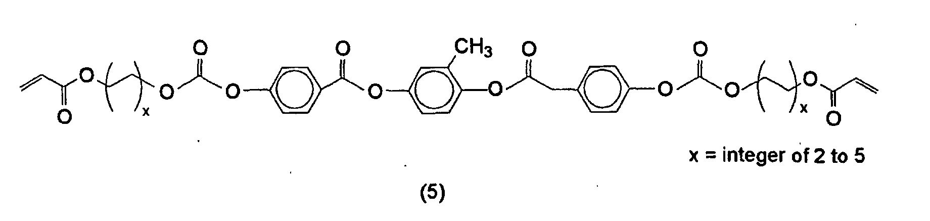
materials include compounds (I) represented by formula
(1) and compounds which will be described later. A
mixture of two compounds covered by formula (1) may also
be used as compound (I).
The polymerizable liquid crystal material may also
be a mixture of two or more compounds covered by formula
(1) and the compounds which will be described later.
In formula (1) which represents compound (I), R1
and R2 each represent a hydrogen atom or a methyl group,
and X preferably represents a chlorine atom or a methyl
group. a and b showing the chain length of the alkylene
group as a spacer of compound (I) are preferably in the
range of 2 to 9 from the viewpoint of developing liquid
crystallinity.
In the above embodiment, examples of polymerizable
liquid crystal monomers have been described. In the
present invention, however, for example, polymerizable
liquid crystal oligomers and polymerizable liquid
crystal polymeric materials may also be used.
Conventional polymerizable liquid crystal oligomers and
polymerizable liquid crystal polymeric materials may be
properly selected and used.
(2) Chiral dopant
In the present invention, when the above optical
device is a circularly polarized light controlling
optical device, that is, when the optical function layer
is a cholesteric layer and the polymerizable liquid
crystal material has nematic regularity or smectic
regularity, a chiral dopant should be added in addition
to the polymerizable liquid crystal material.
The polymerizable chiral dopant used in the present
invention refers to a low-molecular compound which has
an optically active site and a molecular weight of not
more than 1,500. The chiral dopant is mainly used for
inducing a helical pitch in positive uniaxial nematic
regularity developed by compound (I). So far as this
object can be attained, any low-molecular compound may
be used as the chiral dopant without particular
limitation. Specifically, any low-molecular compound may
be used so far as the compound is compatible in a
solution or melted state with compound (I) or the above
compound, does not sacrifice the liquid crystallinity of
the polymerizable liquid crystal material, which can
have nematic regularity, and can induce a desired
helical pitch in the nematic regularity. The presence of
a polymerizable functional group at both ends of the
molecule is preferred from the viewpoint of providing
highly heat resistant optical device. For the chiral
dopant used for inducing a helical pitch in the liquid
crystal, any chirality should be found at least in the
molecule. The chiral dopant having an optically active
site incorporated in the liquid crystalline composition
according to the present invention is preferably a
chiral dopant which is significantly effective in
inducing a helical pitch in the nematic regularity.
Specifically, the use of low-molecular compounds (II)
represented by formula (2), (3), or (4), which have
axial asymmetry in their molecule, is preferred.

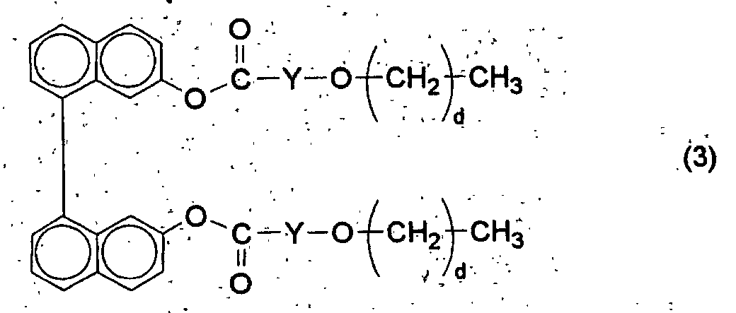







In formula (2), (3), or (4) which represents chiral
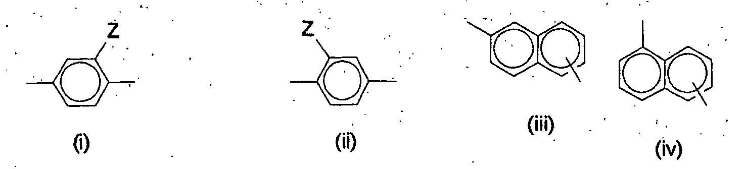
dopant (II), R4 represents a hydrogen atom or a methyl
group. Y represents any one of formulae (i) to (xxiv),
preferably any one of formulae (i) , (ii), (iii), (v),
and (vii). c and d, which represent the chain length of
the alkylene group, are preferably in the range of 2 to
9. When c and d are less than 2 or not less than 10, the
liquid crystallinity is less likely to be developed.
The optimal amount of the chiral dopant
incorporated in the polymerizable liquid crystal
material according to the present invention is
determined by taking into consideration the helical
pitch inducing ability and the cholesteric nature of the
finally obtained circularly polarized light controlling
optical device. Specifically, although the amount of the
chiral dopant incorporated significantly varies
depending upon the polymerizable liquid crystal material
used, the amount of the chiral dopant may be in the
range of 1 to 20 parts by mass based on 100 parts by
mass in total of the polymerizable liquid crystal
material. When the amount of the chiral dopant
incorporated is below the lower limit of the above-defined
amount range, in some cases, satisfactory
cholesteric nature cannot be imparted to the
polymerizable liquid crystal material. On the other hand,
when the amount of the chiral dopant incorporated is
above the upper limit of the above-defined amount range,
the alignment of molecules is inhibited. This possibly
adversely affects curing by the application of an
actinic radiation.
In the present invention, the chiral dopant is not
necessarily polymerizable. When the heat stability and
the like of the optical function layer are taken into
consideration, however, the use of a polymerizable
chiral dopant, which can be polymerized with the
polymerizable liquid crystal material to anchor the
cholesteric regularity, is preferred. In particular, the
presence of a polymerizable functional group at both
ends of the molecule is preferred from the viewpoint of
providing highly heat resistant optical devices.
<Photopolymerization initiator>
In the present invention, a photopolymerization
initiator is preferably added to the polymerizable
liquid crystal material. For example, when the
polymerizable liquid crystal material is polymerized by
electron beam irradiation, the use of a
photopolymerization initiator is in some cases
unnecessary. In the case of a generally used curing
method, for example, curing by ultraviolet (UV)
irradiation, a photopolymerization initiator is
generally used for polymerization acceleration purposes.
In addition to the photopolymerization initiator, a
sensitizer may be added in such an amount range that is
not detrimental to the object of the present invention.
The photopolymerization initiator may be generally
added in an amount of 0.5 to 10% by mass to the
polymerizable liquid crystal material according to the
present invention.
3. Liquid crystal regularity
In the present invention, an optical function layer
formed by curing the polymerizable liquid crystal
material while retaining predetermined liquid crystal
regularity is used.
Nematic regularity, smectic regularity, and
cholesteric regularity may be mentioned as the liquid
crystal regularity. When the optical device is a
retardation layer laminate, the optical function layer
has nematic regularity or smectic regularity. On the
other hand, when the optical device is a circularly
polarized light controlling optical device, the optical
function layer has cholesteric regularity.
The regularity is basically determined by liquid
crystal regularity, which the polymerizable liquid
crystal material per se develops, and whether or not a
chiral dopant is used.
The liquid crystal regularity can be provided by
forming, on a supporting substrate having an aligning
ability, a layer, for liquid crystal layer formation,
comprising the above polymerizable liquid crystal
material and an optional polymerizable chiral dopant and
allowing the molecules of the liquid crystal to align
along the aligning ability of the supporting substrate.
The liquid crystal layer can be converted to an optical
function layer by applying an actinic radiation to the
liquid crystal layer in such a state that the liquid
crystal regularity is retained, thereby curing the
liquid crystal layer.
4. Percentage reduction in thickness of optical function
layer upon heating
The present invention is characterized in that the
percentage reduction in thickness of the above optical
function layer, when heated for 60 min at the same
temperature as applied in the heat treatment of the
optical device, is not more than 5%, preferably not more
than 3%, particularly preferably not more than 1%. For
example, in 'the case where the optical device is a phase
difference plate or a circularly polarized light
controlling optical device, when the percentage
reduction in layer thickness is in this range, there is
no fear of causing a significant change in retardation
value or center reflection wavelength, which are
important optical properties of the optical device, even
upon heating of image display devices or the- like using
the optical device in the production thereof. Therefore,
the optical device according 'to the present invention
can be used even in the case where the optical device is
exposed to heat in a step after mounting the optical
device.
5. Specific embodiments of optical device
Specific embodiments of the optical device
according to the present invention include a retardation
layer laminate comprising a retardation layer as the
optical function layer and a circularly polarized light
controlling optical device comprising a cholesteric
layer as the optical function layer. The retardation
layer laminate and the circularly polarized light
controlling optical device will be described.
<Retardation layer laminate>
In the present invention, when the optical device
is a retardation layer laminate, the retardation layer
laminate may comprise a support and a retardation layer
provided on the support and formed by curing a
polymerizable liquid crystal material while retaining
nematic regularity, smectic regularity, or cholesteric
regularity, wherein the percentage change in retardation
value of the retardation layer, when heated for 60 min
at the same temperature as the predetermined temperature
in the heat treatment, is not more than 5%, preferably
not more than 3%, particularly preferably not more than
1%.
Thus, in the optical device according to the
present invention, the change in layer thickness upon
heating is so small that, when the optical device is
used as a retardation layer laminate, the change in
retardation value upon exposure of the retardation layer
laminate to heat is advantageously very small.
The retardation layer laminate according to the
present invention, when exposed to heat, undergoes only
a very small change in retardation value. Therefore, the
laminate can be used even in the case where, after the
incorporation of the retardation layer laminate, heat
treatment should be carried out, for example, for the
formation of an ITO film. This is advantageous in that
the utilization range of the retardation layer laminate
according to the present invention can be greatly
expanded.
A suitable retardation layer may be formed by
dissolving the liquid crystal material comprising a
polymerizable liquid crystal monomer and a
photopolymerization initiator in a solvent to prepare a
solution, coating the solution, and curing the coating.
In this case, the polymerizable liquid crystal monomer
and the photopolymerization initiator may be those as
described above.
The other construction is the same as described
above, and, thus, the description thereof will be
omitted.
<Circularly polarized light controlling optical
device>
In the present invention, 'when the optical device
is a circularly polarized light controlling optical
device, the circularly polarized light controlling
optical device may comprise a support and a cholesteric
layer provided on the support and formed by curing a
polymerizable liquid crystal material while retaining
cholesteric regularity, wherein the percentage change in
center reflection wavelength of the cholesteric layer,
when heated for 60 min at the same temperature as the
predetermined temperature in the heat treatment, is not
more than 5%, preferably not more than 3%, particularly
preferably not more than 1%.
Also in this case, since the change in layer
thickness is associated with the change in center
reflection wavelength of the cholesteric layer, when the
optical device is used as a circularly polarized light
controlling optical device, the change in center
reflection wavelength can be made very small even upon
heating of an image display device using the optical
device in the production thereof.
In the circularly polarized light controlling
optical device, as described above, the change in center
reflection wavelength upon heating is so small that the
circularly polarized light controlling optical device
according to the present invention can be used even in
the case where, after the incorporation of the
circularly polarized light controlling optical device,
for example, as a color filter, in an image processing
device, heat treatment should be carried out, for
example, for the formation of an ITO film. This is
advantageous in that the utilization range of the
circularly polarized light controlling optical device
can be greatly expanded.
A suitable cholesteric layer in the circularly
polarized light controlling optical device may be formed
by dissolving a liquid crystal material comprising a
polymerizable liquid crystal monomer, a polymerizable
chiral dopant, and a photopolymerization initiator in a
solvent to prepare a solution, coating the solution, and
curing the coating. In this case, the polymerizable
liquid crystal monomer, the polymerizable chiral dopant,
and the photopolymerization initiator may be those as
described above.
The other construction is the same as described
above, and, thus, the description thereof will be
omitted.
<Heat treatment method>
The method for heat treating an optical device
according to the present invention is characterized by
heat treating an optical device, comprising a supporting
substrate and an optical function layer provided on the
supporting substrate and formed by curing a
polymerizable liquid crystal material while retaining
predetermined liquid crystal regularity, at a
temperature falling within a predetermined temperature
range or by heat treating the optical device at or above
a temperature which corresponds to an isotropic layer
before polymerizing the polymerizable liquid crystal
material, thereby imparting heat resistant to the
optical device. In this case, preferably, the heat
treatment is carried out for 10 to 60 min. This heat
treatment can move the liquid crystal component or the
chiral component, which remains uncured or does not form
a satisfactory three-dimensional network structure, to a
stable state (position) within the layer.
In the method for heat treating an optical device
according to the present invention, the heat treatment
is previously carried out at a predetermined temperature,
and impurities within the optical function layer are
removed by this heat treatment. Therefore, even when
heating is carried out in a later stage, that is, even
when, after mounting the optical device subjected to the
heat treatment according to the present invention,
heating is carried out, for example, in an image
processing device for the formation of a transparent
electrode, since the heat treatment is previously
carried out, there is no change in layer thickness of
the optical device. Consequently, there is no fear of
causing a change in various optical functions associated
with the layer thickness. Thus, in mounting the heat
treated optical device, for example, on an image
processing device, there is no restriction on mounting
position and mounting timing. This offers an advantage
that the degree of freedom in the production of an image
processing device and the degree of freedom in product
design can be significantly improved.
The production process of an optical device
according to the present invention including the above
heat treatment method will be described.
Figs. 1 to 6 show an embodiment of the production
process of an optical device according to the present
invention.
In this embodiment, a supporting substrate 3 having
an aligning ability is first provided. The supporting
substrate 3 comprises a transparent substrate 1 and an
aligning film 2 provided on the transparent substrate 1
(step of providing supporting substrate, see Fig. 1).
Next, a coating liquid for liquid crystal layer
formation prepared by dissolving a polymerizable liquid
crystal material and a photopolymerization initiator in
a solvent is coated onto the supporting substrate 3
having an aligning ability, the coating is dried to
remove the solvent, and the coating is kept at a
temperature suitable for developing a liquid crystal
phase to form a liquid crystal layer 4 (step of forming
liquid crystal layer, see Fig. 2). By virtue of the
action of the aligning film 2, the liquid crystal layer
has liquid crystal regularity.
Upon the application of ultraviolet light 5 to the
liquid crystal layer 4 having liquid crystal regularity,
the polymerizable liquid crystal material in the liquid
crystal layer is polymerized by radicals generated from
the photopolymerization initiator to convert the. liquid
crystal layer 4 to an optical function layer 6 (step of
forming optical function layer, see Figs. 3 and 4).
The optical device 8 comprising the optical
function layer 6 provided on the supporting substrate 3'
is then kept, for example, in an oven at a predetermined
temperature, whereby heat 7 is applied to the optical
device 8 for heat treatment (step of heat treatment, see
Fig. 5).
The heat treated optical device 8 thus obtained has
dimensional stability against heat and, in its turn, is
stable in various optical functions (see Fig. 6).
The production process of an optical device
according to the present invention will be described
together with the detailed description of the heat
treatment method according to the present invention.
1. Step of providing supporting substrate
In the production of the optical device according
to the present invention, a supporting substrate having
an aligning ability should be first provided. The
supporting substrate having an aligning ability may be
constituted by a substrate which as such has an aligning
ability. Alternatively, as shown in Fig. 1, the
supporting substrate 3 having an aligning ability may
comprise an aligning film 2 provided on a transparent
substrate 1. These are the same as those described above
in the column of <Optical device>, and the description
thereof will be omitted.
2. Step of forming liquid crystal layer
In the present invention, as shown in Fig. 2, a
liquid crystal layer 4 is formed on the supporting
substrate 3 having an aligning ability.
In the present invention, the liquid crystal layer
is formed of a polymerizable liquid crystal material and
is not particularly limited so far as the liquid crystal
layer can take liquid crystal phases having various
types of liquid crystal regularity.
The liquid crystal layer may be formed, for example,
by the following method. Specifically, a layer for
liquid crystal layer formation is generally formed by
dissolving a polymerizable liquid crystal material, such
as a polymerizable monomer, and optional additives, such
as a chiral dopant and a photopolymerization initiator,
in a solvent to prepare a coating liquid for liquid
crystal layer formation and coating the coating liquid.
Coating methods usable herein include spin coating,
roll coating, slide coating, printing, dipping/pulling-up
coating, and curtain coating (die'coating).
After the formation of the layer for liquid crystal
layer formation, the solvent is removed to form a liquid
crystal layer having various types of liquid crystal
regularity. Methods usable for removing the solvent
include, for example, removal under reduced pressure or
removal by heating, and a combination of these methods.
In the present invention, the method for forming a
liquid crystal layer is not limited to the above method
using the coating liquid for liquid crystal layer
formation. For example, a method may be adopted wherein
a dry film formed of a liquid crystal material is
laminated on a supporting substrate having an aligning
ability and the laminate is then heated to impart liquid
crystal regularity. In the present invention, however,
for example, from the viewpoint of easy process, the
above method using the coating liquid for liquid crystal
layer formation is preferred.
The polymerizable liquid crystal material, the
chiral dopant, and the photopolymerization initiator
used in the coating liquid for liquid crystal layer
formation are the same as those described above in the
column of <Optical device>, and the description thereof
will be omitted. The solvent and other additives used in
the coating liquid for liquid crystal layer formation
will be described.
<Solvent>
The solvent usable in the coating liquid for liquid
crystal layer formation is not particularly limited so
far as the solvent can dissolve the polymerizable liquid
crystal material and the like and is not detrimental to
the aligning ability on the supporting substrate having
an aligning ability.
The use of a single solvent sometimes results in
unsatisfactory solubility of the polymerizable liquid
crystal material and the like or, as described above,
results in the attack of the supporting substrate having
an aligning ability. The use of a mixture of two or more
solvents, however, can avoid such troubles. Suitable
concentration of the polymerizable liquid crystal
material in the solution varies depending upon the
solubility of the liquid crystalline composition and the
film thickness of the circularly polarized light
controlling optical device to be produced and thus
cannot be unconditionally specified. However, the
concentration of the polymerizable liquid crystal
material in the solution is generally in the range of 5
to 60% by mass.
A surfactant and the like may be added for
coatability improvement purposes to the coating liquid
for liquid crystal layer formation.
The amount of the surfactant added is generally in
the range of 0.01 to 1% by mass based on the liquid
crystalline composition contained in the solution,
although the amount of the surfactant added varies
depending upon the type of the surfactant, the type of
the polymerizable liquid crystal material, the type of
the solvent, and the type of the supporting substrate
having an aligning ability to be coated with the
solution.
3. Step of forming optical function layer
In the present invention, upon the application of
an actinic radiation to a liquid crystal layer, composed
mainly of a polymerizable liquid crystal material,
formed in the step of forming a liquid crystal layer,
the liquid crystal layer is cured in such a state that
liquid crystal regularity is retained. Thus, optical
function layers having various optical functions can be
formed.
The actinic radiation applied at that time is not
particularly limited so far as the actinic radiation can
polymerize the polymerizable liquid crystal material,
the polymerizable chiral dopant and the like. In general,
however, light with a wavelength of 250 to 450 nm is
applied.
The irradiation intensity may be properly regulated
depending upon the composition of the polymerizable
liquid crystal material constituting the liquid crystal
layer and the amount of the photopolymerization
initiator.
4. Step of transfer
In the production process according to the present
invention, if necessary, the step of transferring the
optical function layer, provided on the supporting
substrate having an aligning ability, onto a receiving
object may be provided after the step of forming an
optical function layer.
The step of transfer may be carried out according
to need, for example, in the case where the optical
function layer is used in combination with other
layer(s) or in the case where, although the optical
function layer is preferably formed on a nonflexible
supporting substrate, the optical function layer is
intended to be used in such a state that the optical
function layer is provided on the surface of a flexible
film.
The transfer is carried out by bringing the surface
of the receiving object into contact with the surface of
the optical function layer formed in the step of forming
an optical function layer (see Figs. 2 and 3).
Transfer methods usable herein include, for example,
a method wherein an adhesive layer is previously formed
on the surface of the receiving object or the surface of
the optical function layer and the optical function
layer is transferred by taking advantage of the adhesive
power, and a method wherein the aligning film or the
like in the supporting substrate is rendered easily
separable.
Further methods effective for the transfer include
a method wherein the optical function layer is formed so
that the hardness of the surface of the optical function
layer on its side, with which the receiving object comes
into contact, is lower than the hardness of the surface
of the optical function layer on its supporting
substrate side and the optical function layer is
transferred from this assembly onto the receiving object,
and a method wherein the optical function layer is
formed so that the percentage residual double bond in
the surface of the optical function layer on its
receiving object side is higher than that in the surface
of the optical function layer on its supporting
substrate side and the optical function layer is
transferred from this assembly onto the receiving object.
The degree of polymerization on the surface side of the
optical function layer can be made lower than that on
the substrate side, for example, by using a
photopolymerization initiator, which has such oxygen
dependency that causes a lowering in polymerization rate
in the presence of oxygen, in the polymerizable liquid
crystal material and conducting polymerization under
conditions such that oxygen comes into contact with only
the surface side of the optical function layer.
The receiving object used in this step may be
properly selected depending upon applications of the
optical device. In general, however, the use of a
transparent material, that is, a transparent substrate,
is suitable.
This transparent substrate may be the same as that
described in the above column of "Supporting substrate
having aligning ability," and, thus, the description
thereof will be omitted.
5. Step of heat treatment
The present invention is characterized in that the
step of heat treatment is carried out after the step of
forming an optical function layer, and the method for
heat treating an optical device according to the present
invention includes the heat treatment method in this
step.
Specifically, the heat treatment of the optical
device according to the present invention is
characterized in that the optical device comprising the
support and the optical function layer provided on the
support and formed in the step of forming an optical
function layer is heat treated at a predetermined
temperature. As described above, when the support is,
for example, a polymeric stretched film, the heat
treatment temperature is preferably in the range of
about 80 to 120°C, more preferably in the range of 90 to
120°C, still more preferably in the range of 90 to 110°C.
On the other hand, when the support is, for example, a
glass substrate, the heat treatment temperature is
preferably in the range of about 180 to 240°C, more
preferably in the range of 190 to 230°C, still more
preferably in the range of 200 to 220°C.
The above temperature is generally determined by
taking into consideration the heating temperature
applied, for example, in the formation of an ITO
electrode or in the formation of a polyimide film as an
aligning film in the production of an image processing
device. Specifically, stable film thickness and, in its
turn, stable various functions of the optical device
associated with the film thickness at the temperature
applied in the production process of the image
processing device are required of the optical device to
be heat treated. Accordingly, the heat treatment is
preferably carried out at a temperature between at least
the temperature applied in the production process of an
image processing device, to which the optical device is
used, and a temperature at least 10°C above the
temperature applied in the production process of the
image processing device.
In the present invention, the heat treatment is
carried out at the above temperature for 10 to 60 min,
preferably 15 to 45 min, particularly preferably 20 to
40 min.
The heat treatment time may be such that internal
impurities can be removed. From this viewpoint, the heat
treatment is carried out for the above time period range.
The heat treatment may be carried out in
conventional heat treatment equipment such as an oven.
In the present invention, the polymerizable liquid
crystal material preferably contains a
photopolymerization initiator. This is because, as
described above, the change in thickness of the optical
function layer upon heating is minimized by preventing a
lowering in the layer thickness caused by the removal of
impurities having no chemical bond to the main chain
present within the optical function layer at the time of
heating. Therefore, when residues such as
photopolymerization initiators are previously present
within the optical function layer, the advantage of the
heat treatment method according to the present invention
can be utilized best.
The above heat treatment method is effective
particularly in a retardation layer laminate wherein the
optical function layer is a retardation layer. A change
in thickness of the retardation layer upon heating in
the production process of an image display device
results in a significant change in retardation value of
the retardation layer. The change in retardation value
of the retardation layer disadvantageously poses a
severe problem associated with optical design, and the
retardation layer laminate, which causes a change in
retardation value, cannot generally be used.
In the heat treatment method according to the
present invention, by virtue of the above previous heat
treatment, the change in retardation value can be'
minimized even upon exposure of the retardation layer to
heat, for example, in the production process of an image
processing device. Therefore, in the production process,
the optical device can be used even when heat is applied.
This can advantageously significantly expand
applications of the retardation layer laminate.
Further, the heat treatment method is also
effective particularly for a circularly polarized light
controlling optical device wherein the optical function
layer is a cholesteric layer. In this cholesteric layer,
the center reflection wavelength depends upon the layer
thickness. Therefore, in the cholesteric layer as with
the retardation layer, the center reflection wavelength,
which is an important optical property, does not undergo
a change even upon heating in the production of the
circularly polarized light controlling optical device.
This can advantageously significantly expand
applications of the circularly polarized light
controlling optical device.
It should be noted that the present invention is
not limited to the above embodiments. The above
embodiments are illustrative only, and variations and
modifications fall within the technical scope of the
present invention so far as they have substantially the
same construction as and the same function and effect as
the technical idea described in the claims of the
present invention.
EXAMPLES
The following examples further illustrate the
present invention.
A. Cholesteric layer
(Preparation of coating liquid for liquid crystal
layer formation)
A powder of a 100 : 5 : 5 (% by mass) mixture of a
polymerizable liquid crystal material, a chiral dopant,
and a photopolymerization initiator was dissolved at a
concentration of 30% by mass in toluene to prepare a
coating liquid for liquid crystal layer formation. The
polymerizable liquid crystal material, the chiral dopant,
and the photopolymerization initiator used were as
follows.
- Polymerizable liquid crystal material: A
polymerizable liquid crystal monomer represented by
formula (5) which has a polymerizable functional group
in its ends and exhibits nematic liquid crystallinity at
50 to 100°C
- Chiral dopant: A polymerizable chiral dopant
produced by attaching acrylate to both ends of a mesogen
of a compound represented by formula (6) through a
spacer to render the compound polymerizable
- Photopolymerization initiator: IRG 907 (tradename,
manufactured by Ciba Specialty Chemicals, K.K.)
(Formation of aligning film)
Next, a solution for the formation of an aligning
film composed mainly of polyimide was spin coated onto a
0.7 mm-thick glass substrate. The solvent was evaporated,
and the coating was then post-baked at 200°C, followed by
rubbing by a conventional method to form an aligning
film.
Separately, a solution for the formation of an
aligning film composed mainly of polyvinyl alcohol was
bar coated onto a 75 µm-thick TAG film. The solvent was
evaporated, and the coating was then post-baked at 100°C,
followed by rubbing by a conventional method to form an
aligning film.
(Formation of cholesteric layer)
The above coating liquid for liquid crystal layer
formation was spin coated onto the aligning film of the
polyimide. The solvent was then evaporated. Thereafter,
liquid crystal molecules were aligned under conditions
of 80°C and 3 min, and selective reflection
characteristic of a cholesteric structure could be
confirmed. Ultraviolet light (UV) was then applied to
the coating to cause polymerization, thereby forming a
cholesteric layer. Thus, sample 1 was prepared.
Separately, the above coating liquid for liquid
crystal layer formation was bar coated onto the aligning
film of polyvinyl alcohol. The solvent was then
evaporated. Thereafter, liquid crystal molecules were
aligned under conditions of 80°C and 3 min, and selective
reflection characteristic of a cholesteric structure
could be confirmed. Ultraviolet light (UV) was then
applied to the coating to cause polymerization, thereby
forming a cholesteric layer. Thus, sample 2 was prepared.
For sample 1 thus obtained, a part of the sample
was heat treated at 200°C for 60 min, was then self-cooled
to room temperature, and was allowed to stand for
one day (Example 1), while the other part of the sample
was not heat treated (Comparative Example 1).
For sample 2 thus obtained, a part of the sample
was heat treated at 100°C for 60 min, was then self-cooled
to room temperature, and was allowed to stand for
one day (Example 2), while the other part of the sample
was not heat treated (Comparative Example 2).
(Evaluation)
The sample of Example 1 and the sample of
Comparative Example 1 were measured for selective
reflection center wavelength, were then heated at 200°C
for 60 min, and were again measured for selective
reflection center wavelength, and the percentage change
in center wavelength, that is, the percentage difference
in center wavelength between the sample before the heat
treatment and the sample after the heat treatment, was
determined. The results were as follows.
· Example 1: 1% change to shorter wavelength side
· Comparative Example 1: 6% change to shorter
wavelength side
The sample of Example 2 and the sample of
Comparative Example 2 were measured for selective
reflection center wavelength, were then heated at 100°C
for 60 min, and were again measured for selective
reflection center wavelength. The percentage change in
center wavelength was determined as described above. The
results were as follows.
· Example 2: 1% change to shorter wavelength side
· Comparative Example 2: 6% change to shorter
wavelength side
B. Retardation layer 1
(Preparation of coating liquid for liquid crystal
layer formation and formation of aligning film)
A coating liquid for liquid crystal layer formation
was prepared in the same manner as in the above item A,
except that any chiral dopant was not used and the
mixing ratio of the polymerizable liquid crystal
material to the photopolymerization initiator was 100 :
5 (% by mass). Further, an aligning film was formed in
the same manner as in the above item A.
(Formation of retardation layer)
The coating liquid for liquid crystal layer
formation was spin coated or bar coated on the above
aligning film. The solvent was then evaporated.
Thereafter, liquid crystal molecules were nematically
aligned under conditions of 80°C and 3 min. Ultraviolet
light (UV) was then applied to the coating to cause
polymerization, thereby forming a retardation layer 1.
Thus, samples 3 and 4 were prepared.
For sample 3 having a nematic structure thus
obtained, a part of the sample was heat treated at 200°C
for 60 min, was then self-cooled to room temperature,
and was allowed to stand for one day (Example 3), while
the other part of the sample was not heat treated
(Comparative Example 3). Further, for sample 4 thus
obtained, a part of the sample was heat treated at 100°C
for 60 min, was then self-cooled to room temperature,
and was allowed to stand for one day (Example 4), while
the other part of the sample was not heat treated
(Comparative Example 4).
(Evaluation)
The sample of Example 3 and the sample of
Comparative Example 3 were measured for retardation
value, were then heated at 200°C for 60' min, and were
again measured for retardation value, and the percentage
change in retardation value, that is, the percentage
difference in retardation value between the sample
before the heat treatment and the sample after the heat
treatment, was determined. The results were as follows.
· Example 3: 1% change in retardation value
· Comparative Example 3: 6% change in retardation
value
The sample of Example 4 and the sample of
Comparative Example 4 were measured for retardation
value, were then heated at 100°C for 60 min, and were
again measured for retardation value. The percentage
change in retardation value was determined in the same
manner as described above. The results were as follows.
· Example 4: 1% change in retardation value
· Comparative Example 4: 6% change in retardation
value
C. Retardation layer 2
(Preparation of coating liquid for liquid crystal
layer formation and formation of aligning film)
A coating liquid for liquid crystal layer formation
was prepared in the same manner as in the above item A,
except that the mixing ratio among the polymerizable
liquid crystal material, the chiral dopant, and the
photopolymerization initiator was 100 : 15 : 5 (% by
mass). Further, an aligning film was formed in the same
manner as in the above item A.
(Formation of retardation layer)
The coating liquid for liquid crystal layer
formation was spin coated on the aligning film of
polyimide. The solvent was then evaporated. Thereafter,
liquid crystal molecules were aligned under conditions
of 80°C and 3 min. Ultraviolet light (UV) was then
applied to the coating to cause polymerization, thereby
forming a cholesteric layer. Thus, sample 5 was prepared.
Since the content of the chiral dopant component in the
above coating liquid for liquid crystal layer formation
was higher than that in the coating liquid for liquid
crystal layer formation used in Example 1, the selective
reflection center wavelength of the sample 5 thus
prepared was in the ultraviolet region. The retardation
layer 2 thus formed could function as a negative phase
difference compensating plate.
The above coating liquid for liquid crystal layer
formation was bar coated onto the aligning film of
polyvinyl alcohol. The solvent was then evaporated.
Thereafter, liquid crystal molecules were aligned under
conditions of 80°C and 3 min. UV was then applied to the
coating to cause polymerization, thereby forming a
cholesteric layer. Thus, sample 6 was prepared. Also
for sample 6, the selective reflection center wavelength
was in the ultraviolet region.
For sample 5 having a cholesteric structure thus
obtained, a part of the sample was heat treated at 200°C
for 60 min, was then self-cooled to room temperature,
and was allowed to stand for one day (Example 5), while
the other part of the sample was not heat treated
(Comparative Example 5). Further, for sample 6 thus
obtained, a part of the sample was heat treated at 100°C
for 60 min, was then self-cooled to room temperature,
and was allowed to stand for one day (Example 6), while
the other part of the sample was not heat treated
(Comparative Example 6).
(Evaluation)
The sample of Example 5 and the sample of
Comparative Example 5 were measured for retardation
value, were then heated at 200°C for 60 min, and were
again measured for retardation value, and the percentage
change in retardation value, that is, the percentage
difference in retardation value between the sample
before the heat treatment and the sample after the heat
treatment, was determined. The results were as follows.
· Example 5: 1% change in retardation value
· Comparative Example 5: 6% change in retardation
value
The sample of Example 6 and the sample of
Comparative Example 6 were measured for retardation
value, were then heated at 100°C for 60 min, and were
again measured for retardation value. The percentage
change in retardation value was determined in the same
manner as described above. The results were as follows.
· Example 6: 1% change in retardation value
· Comparative Example 6: 6% change in retardation
value