EP1441498A2 - Image printing apparatus and method of adjusting and correcting main-scanning offset in image printing apparatus - Google Patents
Image printing apparatus and method of adjusting and correcting main-scanning offset in image printing apparatus Download PDFInfo
- Publication number
- EP1441498A2 EP1441498A2 EP03024971A EP03024971A EP1441498A2 EP 1441498 A2 EP1441498 A2 EP 1441498A2 EP 03024971 A EP03024971 A EP 03024971A EP 03024971 A EP03024971 A EP 03024971A EP 1441498 A2 EP1441498 A2 EP 1441498A2
- Authority
- EP
- European Patent Office
- Prior art keywords
- image
- scanning direction
- clock
- main scanning
- dot clock
- Prior art date
- Legal status (The legal status is an assumption and is not a legal conclusion. Google has not performed a legal analysis and makes no representation as to the accuracy of the status listed.)
- Withdrawn
Links
- 238000007639 printing Methods 0.000 title claims abstract description 216
- 238000000034 method Methods 0.000 title claims description 11
- 230000002441 reversible effect Effects 0.000 claims abstract description 52
- 238000012360 testing method Methods 0.000 claims description 221
- 239000003086 colorant Substances 0.000 claims description 45
- 230000000052 comparative effect Effects 0.000 claims description 15
- 238000012937 correction Methods 0.000 description 69
- 238000001514 detection method Methods 0.000 description 20
- 230000008030 elimination Effects 0.000 description 14
- 238000003379 elimination reaction Methods 0.000 description 14
- 230000001360 synchronised effect Effects 0.000 description 14
- 238000012546 transfer Methods 0.000 description 14
- 238000012545 processing Methods 0.000 description 12
- 230000008602 contraction Effects 0.000 description 10
- 230000007423 decrease Effects 0.000 description 6
- 230000003247 decreasing effect Effects 0.000 description 5
- 230000010354 integration Effects 0.000 description 5
- 238000005259 measurement Methods 0.000 description 4
- 230000010355 oscillation Effects 0.000 description 4
- 230000004075 alteration Effects 0.000 description 3
- 230000007274 generation of a signal involved in cell-cell signaling Effects 0.000 description 3
- 230000003287 optical effect Effects 0.000 description 3
- 230000001629 suppression Effects 0.000 description 3
- 239000000969 carrier Substances 0.000 description 2
- 238000004140 cleaning Methods 0.000 description 2
- 238000010586 diagram Methods 0.000 description 2
- 238000007645 offset printing Methods 0.000 description 2
- 238000010187 selection method Methods 0.000 description 2
- 238000007796 conventional method Methods 0.000 description 1
- 230000001934 delay Effects 0.000 description 1
- 230000003111 delayed effect Effects 0.000 description 1
- 230000000694 effects Effects 0.000 description 1
- 238000004519 manufacturing process Methods 0.000 description 1
- 238000000926 separation method Methods 0.000 description 1
Images






Classifications
-
- H—ELECTRICITY
- H04—ELECTRIC COMMUNICATION TECHNIQUE
- H04N—PICTORIAL COMMUNICATION, e.g. TELEVISION
- H04N1/00—Scanning, transmission or reproduction of documents or the like, e.g. facsimile transmission; Details thereof
- H04N1/04—Scanning arrangements, i.e. arrangements for the displacement of active reading or reproducing elements relative to the original or reproducing medium, or vice versa
- H04N1/047—Detection, control or error compensation of scanning velocity or position
- H04N1/053—Detection, control or error compensation of scanning velocity or position in main scanning direction, e.g. synchronisation of line start or picture elements in a line
-
- H—ELECTRICITY
- H04—ELECTRIC COMMUNICATION TECHNIQUE
- H04N—PICTORIAL COMMUNICATION, e.g. TELEVISION
- H04N1/00—Scanning, transmission or reproduction of documents or the like, e.g. facsimile transmission; Details thereof
- H04N1/04—Scanning arrangements, i.e. arrangements for the displacement of active reading or reproducing elements relative to the original or reproducing medium, or vice versa
- H04N1/113—Scanning arrangements, i.e. arrangements for the displacement of active reading or reproducing elements relative to the original or reproducing medium, or vice versa using oscillating or rotating mirrors
- H04N1/1135—Scanning arrangements, i.e. arrangements for the displacement of active reading or reproducing elements relative to the original or reproducing medium, or vice versa using oscillating or rotating mirrors for the main-scan only
-
- H—ELECTRICITY
- H04—ELECTRIC COMMUNICATION TECHNIQUE
- H04N—PICTORIAL COMMUNICATION, e.g. TELEVISION
- H04N1/00—Scanning, transmission or reproduction of documents or the like, e.g. facsimile transmission; Details thereof
- H04N1/04—Scanning arrangements, i.e. arrangements for the displacement of active reading or reproducing elements relative to the original or reproducing medium, or vice versa
- H04N1/12—Scanning arrangements, i.e. arrangements for the displacement of active reading or reproducing elements relative to the original or reproducing medium, or vice versa using the sheet-feed movement or the medium-advance or the drum-rotation movement as the slow scanning component, e.g. arrangements for the main-scanning
-
- H—ELECTRICITY
- H04—ELECTRIC COMMUNICATION TECHNIQUE
- H04N—PICTORIAL COMMUNICATION, e.g. TELEVISION
- H04N2201/00—Indexing scheme relating to scanning, transmission or reproduction of documents or the like, and to details thereof
- H04N2201/024—Indexing scheme relating to scanning, transmission or reproduction of documents or the like, and to details thereof deleted
- H04N2201/02406—Arrangements for positioning elements within a head
- H04N2201/02439—Positioning method
- H04N2201/02443—Positioning method using adhesive
-
- H—ELECTRICITY
- H04—ELECTRIC COMMUNICATION TECHNIQUE
- H04N—PICTORIAL COMMUNICATION, e.g. TELEVISION
- H04N2201/00—Indexing scheme relating to scanning, transmission or reproduction of documents or the like, and to details thereof
- H04N2201/04—Scanning arrangements
- H04N2201/047—Detection, control or error compensation of scanning velocity or position
- H04N2201/04701—Detection of scanning velocity or position
- H04N2201/0471—Detection of scanning velocity or position using dedicated detectors
-
- H—ELECTRICITY
- H04—ELECTRIC COMMUNICATION TECHNIQUE
- H04N—PICTORIAL COMMUNICATION, e.g. TELEVISION
- H04N2201/00—Indexing scheme relating to scanning, transmission or reproduction of documents or the like, and to details thereof
- H04N2201/04—Scanning arrangements
- H04N2201/047—Detection, control or error compensation of scanning velocity or position
- H04N2201/04701—Detection of scanning velocity or position
- H04N2201/04715—Detection of scanning velocity or position by detecting marks or the like, e.g. slits
- H04N2201/04717—Detection of scanning velocity or position by detecting marks or the like, e.g. slits on the scanned sheet, e.g. a reference sheet
-
- H—ELECTRICITY
- H04—ELECTRIC COMMUNICATION TECHNIQUE
- H04N—PICTORIAL COMMUNICATION, e.g. TELEVISION
- H04N2201/00—Indexing scheme relating to scanning, transmission or reproduction of documents or the like, and to details thereof
- H04N2201/04—Scanning arrangements
- H04N2201/047—Detection, control or error compensation of scanning velocity or position
- H04N2201/04701—Detection of scanning velocity or position
- H04N2201/04732—Detecting at infrequent intervals, e.g. once or twice per line for main-scan control
-
- H—ELECTRICITY
- H04—ELECTRIC COMMUNICATION TECHNIQUE
- H04N—PICTORIAL COMMUNICATION, e.g. TELEVISION
- H04N2201/00—Indexing scheme relating to scanning, transmission or reproduction of documents or the like, and to details thereof
- H04N2201/04—Scanning arrangements
- H04N2201/047—Detection, control or error compensation of scanning velocity or position
- H04N2201/04701—Detection of scanning velocity or position
- H04N2201/04744—Detection of scanning velocity or position by detecting the scanned beam or a reference beam
-
- H—ELECTRICITY
- H04—ELECTRIC COMMUNICATION TECHNIQUE
- H04N—PICTORIAL COMMUNICATION, e.g. TELEVISION
- H04N2201/00—Indexing scheme relating to scanning, transmission or reproduction of documents or the like, and to details thereof
- H04N2201/04—Scanning arrangements
- H04N2201/047—Detection, control or error compensation of scanning velocity or position
- H04N2201/04701—Detection of scanning velocity or position
- H04N2201/04749—Detecting position relative to a gradient, e.g. using triangular-shaped masks, marks or gratings
-
- H—ELECTRICITY
- H04—ELECTRIC COMMUNICATION TECHNIQUE
- H04N—PICTORIAL COMMUNICATION, e.g. TELEVISION
- H04N2201/00—Indexing scheme relating to scanning, transmission or reproduction of documents or the like, and to details thereof
- H04N2201/04—Scanning arrangements
- H04N2201/047—Detection, control or error compensation of scanning velocity or position
- H04N2201/04753—Control or error compensation of scanning position or velocity
- H04N2201/04758—Control or error compensation of scanning position or velocity by controlling the position of the scanned image area
- H04N2201/04767—Control or error compensation of scanning position or velocity by controlling the position of the scanned image area by controlling the timing of the signals, e.g. by controlling the frequency o phase of the pixel clock
- H04N2201/04768—Controlling the frequency of the signals
-
- H—ELECTRICITY
- H04—ELECTRIC COMMUNICATION TECHNIQUE
- H04N—PICTORIAL COMMUNICATION, e.g. TELEVISION
- H04N2201/00—Indexing scheme relating to scanning, transmission or reproduction of documents or the like, and to details thereof
- H04N2201/04—Scanning arrangements
- H04N2201/047—Detection, control or error compensation of scanning velocity or position
- H04N2201/04753—Control or error compensation of scanning position or velocity
- H04N2201/04758—Control or error compensation of scanning position or velocity by controlling the position of the scanned image area
- H04N2201/04767—Control or error compensation of scanning position or velocity by controlling the position of the scanned image area by controlling the timing of the signals, e.g. by controlling the frequency o phase of the pixel clock
- H04N2201/04768—Controlling the frequency of the signals
- H04N2201/04774—Controlling the frequency of the signals using a reference clock or oscillator
-
- H—ELECTRICITY
- H04—ELECTRIC COMMUNICATION TECHNIQUE
- H04N—PICTORIAL COMMUNICATION, e.g. TELEVISION
- H04N2201/00—Indexing scheme relating to scanning, transmission or reproduction of documents or the like, and to details thereof
- H04N2201/04—Scanning arrangements
- H04N2201/047—Detection, control or error compensation of scanning velocity or position
- H04N2201/04753—Control or error compensation of scanning position or velocity
- H04N2201/04794—Varying the control or compensation during the scan, e.g. using continuous feedback or from line to line
- H04N2201/04798—Varying the main-scan control during the main-scan, e.g. facet tracking
Definitions
- the present invention relates to an image printing apparatus which prints a one-line image in the main scanning direction in accordance with image data with reference to a dot clock as the basis of each pixel forming an image, and also prints a one-page image by repeating in the sub-scanning direction one-line image printing performed in the main scanning direction.
- an apparatus for printing a one-line image in the main scanning direction in accordance with image data and printing a one-page image by repeating in the sub-scanning direction one-line image printing performed in the main scanning direction is known.
- Image printing in the main scanning direction in accordance with image data is performed with reference to a clock signal (to be referred to as a "dot clock” hereinafter in this specification) as the basis of each pixel to be formed.
- a clock signal to be referred to as a "dot clock” hereinafter in this specification
- a laser beam modulated in accordance with image data is scanned in the main scanning direction, and an image is concurrently formed on an image carrier rotating in the sub-scanning direction with the laser beam.
- a laser beam is modulated with image data with reference to a clock signal (pixel clock) called a dot clock.
- pixel clock a clock signal
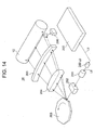
- a laser diode (LD) 260 emits a laser beam LB on the basis of a laser driving signal LS generated on the basis of a dot clock.
- the laser beam LB from the LD 260 passes through a collimator lens 261 and cylindrical lens 262 and is then scanned in the main scanning direction by a polygon mirror 263.
- the laser beam LB scanned by the polygon mirror 263 is adjusted to be scanned at a constant velocity by an fè lens 264.
- the laser beam further passes through a cylindrical lens 265 to strike a photosensitive drum 10.
- Sub-scanning operation is then performed by rotating the photosensitive drum 10 during this main-scanning operation.
- main-scanning operation By repeating main-scanning operation in the sub-scanning direction, a one-page image is printed.
- part of the laser beam LB scanned by the polygon mirror is guided to an index sensor 266 to detect the timing.
- the main-scanning magnification (the magnification in the main scanning direction) may differ from a desired magnification due to the power characteristics and mount precision of various kinds of lens systems, the planarity and mount precision of various kinds of mirrors, the planarity and mount precision of a photosensitive drum as 'an image printing medium (image carrier), individual differences thereof, and the like. That is, an offset may occur in the main scanning direction.
- a plurality of writing units may be provided for the above image printing apparatus to allow it to print a color image. In this case, if offsets in the main scanning direction occur between the respective writing units, a proper color image cannot be printed.
- a halfway point e.g., an intermediate point between the start and the end, may not always coincide with a desired position.
- the factors that cause such halfway offsets include the power characteristics and mount precision of various kinds of lens systems, the planarity and mount precision of various kinds of mirrors, the planarity and mount precision of a photosensitive drum as an image printing medium (image carrier), individual differences thereof, and the like. An enormous cost is required to manufacture and mount these components with high precision without causing any halfway offset.
- the image printing apparatus is an image printing apparatus capable of printing images on the two surfaces of an image recording sheet, even if the distance between the start and the end in the main scanning direction is adjusted to a desired value, a user may recognize the difference between the distances on the two surfaces as an offset.
- the present invention has been made to solve the above problems in the prior art, and has as its object to print images without any halfway offset or obverse/reverse pixel offset at a low cost.
- an image printing apparatus comprising a clock generating section which generates a dot clock as a basis of each pixel forming an image, an image printing section which prints a one-line image in a main scanning direction in accordance with image data with reference to the dot clock output from the clock generating section, and prints a one-page image by repeating in the sub-scanning direction one-line image printing performed in the main scanning direction, and a clock control section which changeably controls a frequency of the dot clock during scanning of one line in the main scanning direction.
- the frequency of the dot clock is changeably controlled during scanning of one line in the main scanning direction.
- an image printing apparatus wherein the clock control section described in the first aspect controls even the number of pixels of one line in the main scanning direction in a case in which the frequency of the dot clock is changed during scanning of one line to be equal to that in a case in which the frequency is not changed.
- the number of pixels of one line in the main scanning direction in a case in which the frequency of the dot clock is changed is controlled to that in a case in which the frequency is not changed.
- an image printing apparatus wherein the clock control section described in the first or second aspect changes the frequency of the dot clock during scanning of one line in the main scanning direction on the basis of a plurality of main-scanning partial offsets in a test image printed by the image printing apparatus in accordance with test image data.
- the frequency of the dot clock is changed during scanning of one line in the main scanning direction on the basis of a plurality of partial main-scanning offsets in test images printed by the image printing apparatus in accordance with test image data.
- an image printing apparatus wherein the image printing apparatus described in the first or second aspect further comprises an offset setting section which sets at least two offsets between distances between test patterns in test images printed by the image printing apparatus in accordance with test image data having test patterns arranged at at least three positions in the main scanning direction and reference distances between comparative test patterns, and the clock control section changes the frequency of the dot clock during scanning of one line in the main scanning direction on the basis of the respective offsets set by the offset setting section.
- At least two offsets are set between the distances between test patterns in test images printed in accordance with test image data having test patterns arranged at at least three positions in the main scanning direction and the reference distances between comparative test patterns, and the frequency of the dot clock is changed during scanning of one line in the main scanning direction on the basis of the respective set offsets.
- an image printing apparatus wherein the clock control section described in the fourth aspect changes the frequency of the dot clock to evenly distribute the offsets to the respective pixels between the test patterns so as to eliminate the offsets.
- offsets are detected between three or more main-scanning test patterns used for image printing, and the frequency of the dot clock is changed to evenly distribute the offsets to the respective pixels so as to eliminate the offsets.
- an image printing apparatus described in the fourth or fifth aspect wherein the image printing apparatus comprises a test patter interval detecting section which computes distances between the test patterns in the test images by detecting positions of the test patterns, and an offset computing section which computes offsets between the distances between the test patterns which are computed by the test pattern interval detecting section and the reference distances between the comparative test patterns, and at least two offsets computed by the offset computing section are set by the offset setting section.
- the positions of test patterns are detected, and the distances between the test patterns are computed.
- the offsets between the computed distances between the test patterns and the reference distances between comparative test patterns are computed. At least two computed offsets are set by the offset setting section.
- the reference distances are distances between the test patterns in the test image data.
- At least two offsets are set between the distances between test patterns in test images printed in accordance with test image data having test patters arranged at at least three positions in the main scanning direction and the reference distances between comparative test patterns, and the distances between the test patterns in the test image data are used as reference distances when the frequency of the dot clock is changed during scanning of one line in the main scanning direction on the basis of the respective set offsets.
- an image printing apparatus wherein the image printing apparatus described in any one of the fourth to sixth aspect prints images on two surfaces of an image recording sheet, and the clock control section changes the frequency of the dot clock when an image is printed on one surface of the image recording sheet or images are printed on the two surfaces.
- images can be printed on the two surfaces of an image recording sheet, and the frequency of the dot clock is changed when an image is to be printed on one surface of the image recording sheet or images are to be printed on the two surfaces.
- the reference distances are distances between the test patterns in the test image data or distances between test patterns in test image data printed on a reverse surface of an image recording sheet when the frequency of the dot clock is changed in printing an image on an obverse surface of the image recording sheet, or the reference distances are distances between the test patterns in the test image data or distances between test patterns in test image data printed on the obverse surface of the image recording sheet when the frequency of the dot clock is changed in printing an image on the reverse surface of the image recording sheet.
- At least two offsets are set between the distances between test patterns in test images printed in accordance with test image data having test patterns arranged at at least three positions in the main scanning direction and the reference distances between comparative test patterns, and the distances between the test patterns in the test images or the distances between test image data printed on the other surface are used as reference distances when the frequency of the dot clock is changed during scanning of one line in the main scanning direction on the basis of the respective set offsets.
- an image printing apparatus wherein the image printing apparatus described in any one of the fourth to ninth aspects prints an image by superimposing an image formed in a first color and an image formed in a second color different from the first color, and the clock control section changes the frequency of the dot clock when one or both of images in the first and second colors are to be printed.
- the frequency of the dot clock is changed for at least one of the colors.
- an image printing apparatus described in the 10 aspect wherein the reference distances are distances between the test patterns in the test image data or distances between test patterns in test image data printed in the second color when the frequency of the dot clock is changed in printing an image in the first color, or the reference distances are distances between the test patterns in the test image data or distances between test patterns in test image data printed in the first color when the frequency of the dot clock is changed in printing an image in the second color.
- At least two offsets are set between the distances between test patterns in test images printed in accordance with test image data having test patterns arranged at at least three positions in the main scanning direction and the reference distances between comparative test patterns, and the distances between the test patterns in the test images or the distances between test image data printed in the other color are used as reference distances when the frequency of the dot clock is changed during scanning of one line in the main scanning direction on the basis of the respective set offsets.
- the clock generating section comprises a fundamental clock generating section which generates a fundamental clock having a predetermined frequency, and a frequency changing section which can change the frequency of the fundamental clock generated by the fundamental clock generating section, and the clock control section changes a frequency of a fundamental clock output from the frequency changing section during scanning of one line in the main scanning direction.
- the clock control section performs control to change the frequency of the fundamental clock output from the frequency changing section during scanning of one line in the main scanning direction.
- an image printing apparatus described in the 12th aspect wherein the frequency changing section has a delay line which generates delay clocks by digitally delaying the fundamental clock, and the clock control section changes the frequency of the dot clock during scanning of one line in the main scanning direction by selecting a predetermined delay clock from the delay line.
- the frequency changing section digitally delays the fundamental clock by the delay line, and the clock control section changes the frequency of the dot clock during scanning of one line in the main scanning direction by selecting a predetermined delay clock from the delay line.
- a main-scanning offset adjusting method for an image printing apparatus which adjusts a main-scanning offset in the image printing apparatus which generates a dot clock as a basis of each pixel forming an image, prints a one-line image in a main scanning direction in accordance with image data with reference to the dot clock, and prints a one-page image by repeating in a sub-scanning direction one-line printing, performed in the main scanning direction, comprising the steps of printing test images in accordance with test image data having test patterns arranged at at least three positions in the main scanning direction, obtaining at least two offsets between distances between the test patterns in the test images and reference distances between comparative test patterns, and setting the respective offsets such that the frequency of the dot clock can be changed during scanning of one line in the main scanning direction on the basis of the respective offsets.
- test images are printed in accordance with test image data having test patterns arranged at at least three positions in the main scanning direction, and at least two offsets are obtained between the distances between the test patterns in the test images and the reference distances between comparative test patterns.
- the respective offsets are set such that the frequency of the dot clock can be changed during scanning of one line in the main scanning direction on the basis of the respective offsets.
- a main-scanning offset correcting method for an image printing apparatus which corrects a main-scanning offset in the image printing apparatus which generates a dot clock as a basis of each pixel forming an image, prints a one-line image in a main scanning direction in accordance with image data with reference to the dot clock, and prints a one-page image by repeating in a sub-scanning direction one-line printing, performed in the main scanning direction, comprising the steps of setting at least two offsets, before image printing, between distances between test patterns in test images printed in accordance with test image data having test patterns arranged at at least three positions in the main scanning direction and reference distances between comparative test patterns, and changing the frequency of the dot clock during scanning of one line in the main scanning direction on the basis of the respective offsets set in the offset setting step during image printing.
- At least two offsets are set between the distances between test patterns in test images printed in accordance with test image data having test patterns arranged at at least three positions in the main scanning direction and the reference distances between comparative test patterns, and the frequency of the dot clock is changed during scanning of one line in the main scanning direction during image printing operation.
- an image printing apparatus including a clock generating section which generates a dot clock as a basis of each pixel forming an image, and an image printing section which prints a one-line image in a main scanning direction in accordance with image data with reference to the dot clock output from the clock generating section, and printing in the sub-scanning direction a one-page image by repeating one-line image printing performed in the main scanning direction, comprising a control section which controls image printing in the main scanning direction such that distances between test patterns in reference images which are arranged at at least three positions in the main scanning direction coincide with distances between test images printed in accordance with test image data corresponding to the reference images.
- image printing in the main scanning direction is controlled such that the distances between test patterns in reference images which are arranged at at least' three positions in the main scanning direction coincide with distances between test images printed in accordance with test image data corresponding to the reference images.
- control section described in the 16th aspect comprises a clock control section which changeably controls the frequency of the dot clock during scanning of one line.
- image printing in the main scanning direction is controlled during scanning of one line such that the distances between test patterns in reference images which are arranged at at least three positions in the main scanning direction coincide with distances between test images printed in accordance with test image data corresponding to the reference images.
- an image printing apparatus for printing images on two surfaces of an image recording sheet, which includes a clock generating section which generates a dot clock as a basis of each pixel forming an image, and an image printing section which prints a one-line image in a main scanning direction in accordance with image data with reference to the dot clock output from the clock generating section, and prints a one-page image by repeating in the sub-scanning direction one-line image printing, performed in the main scanning direction, wherein the frequency of the dot clock can be set to different frequencies depending on whether an image is to be printed on an obverse surface or reverse surface of an image recording sheet.
- the frequency of the dot clock can be set to different frequencies depending on whether an image is to be printed on the obverse or reverse surface of the image recording sheet.
- an image printing apparatus including a clock generating section which generates a dot clock as a basis of each pixel forming an image, a toner image forming section which includes a writing section which forms a one-line image in a main scanning direction in accordance with image data with reference to the dot clock output from the clock generating section, and forms a one-page image by repeating in the sub-scanning direction one-line image printing performed in the main scanning direction, the toner image forming section which forms a toner image on one surface of an image recording sheet, and a fixing section which fixes the toner image formed by the toner image forming section on the image recording sheet, the image printing apparatus printing images on two surfaces of the image recording sheet by causing the toner image forming section to form a toner image on a reverse surface of the image recording sheet having the toner image formed on one surface and causing the fixing section to fix the image, wherein the frequency of the dot clock can be set to different frequencies depending on whether an
- the toner image on the reverse surface is fixed after the toner image formed on the obverse surface is fixed.
- the frequency of the dot clock can be set to different frequencies depending on whether an image is to be printed on the obverse or reverse surface of the image recording sheet.
- an image printing apparatus described in the 19th aspect wherein the frequency of the dot clock can be set to a given frequency when an image is to be printed on at least one of obverse and reverse surfaces of an image recording sheet.
- the toner image on the reverse surface is fixed after the toner image formed on the obverse surface is fixed.
- the frequency of the dot clock can be set to different frequencies depending on whether an image is to be printed on the obverse or reverse surface of the image recording sheet.
- changing the frequency of a dot clock means changing the leading or trailing edge timing of the dot clock to a desired timing such as a given timing during scanning of one line or a timing corresponding to each image printing surface or image printing color in order to change the position of a pixel printed in accordance with the dot clock.
- a desired timing such as a given timing during scanning of one line or a timing corresponding to each image printing surface or image printing color in order to change the position of a pixel printed in accordance with the dot clock.
- the image printing apparatus scans a laser beam modulated in accordance with image data in the main scanning direction, and forms an image on an image carrier which rotates in the sub-scanning direction.
- the laser beam is modulated with the image data with reference to a pixel clock called a dot clock.
- Fig. 7 is a view showing the arrangement of the print engine of the image printing apparatus according to this embodiment.
- Fig. 7 shows the image printing apparatus capable of printing images on the two surfaces of an image recording sheet as a specific example. Note that the image printing apparatus capable of printing images on the two surfaces of an image recording sheet can print an image on only one surface of an image recording sheet.
- reference numeral 10 denotes a photosensitive drum serving as an image carrier on which a toner image is formed; and 11, a charging electrode for applying a predetermined potential to the photosensitive drum 10.
- Reference numeral 20 denotes a writing unit for forming an electrostatic latent image on the surface of the photosensitive drum 10 by scanning a laser beam in accordance with image information.
- Reference numeral 30 denotes a developing device for forming a toner image by developing the electrostatic latent image formed on the surface of the photosensitive drum 10 with a developer (toner).
- Reference numeral 40 denotes a transfer/separation electrode for transferring the toner image from the photosensitive drum 10 to an image recording sheet, and separating the transfer sheet from the photosensitive drum 10. Note that an illustration of a cleaning section and the like is omitted.
- Reference numeral 50 denotes a paper feed section in which image recording sheets are stored.
- Fig. 7 shows paper feed cassettes 51 and 52 of the paper feed section 50. Note that the number of paper feed cassettes is not limited to this.
- Reference numerals 61 to 68 denote convey devices such as convey rollers and path switching device.
- Reference numeral 61 denotes a feed roller for feeding an image recording sheet from a paper feed cassette; 62, a convey path along which an image recording sheet from the paper feed section 50 (51 or 52) travels; 63a and 63b, registration rollers for feeding an image recording sheet at the timing of image printing; 65, a path switching device which switches between delivery and circulation of an image recording sheet; 66a, 66b, 67a, 67b, 68a, and 68b, inversion rollers for inverting the obverse and reverse surfaces of an image recording sheet; and 69a and 69b, delivery rollers for delivering an image recording sheet outside the apparatus.
- Reference numeral 70 denotes a fixing unit for fixing (heat fusing) a toner image on an image recording sheet with heat and pressure.
- the fixing unit 70 fixes a toner image on an image recording sheet while clamping/conveying it with a heat roller 71 (or 72) and a pressure roller 72 (or 71).
- the image printing apparatus shown in Figs. 14 and 7 is assumed as a specific example of the image printing apparatus according to this embodiment. That is, the image printing apparatus of the first embodiment is an image printing apparatus capable of printing an image on at least one surface of an image. recording sheet. Note that this apparatus may either be a monochrome image printing apparatus or color image printing apparatus.
- Fig. 1 shows a writing unit circuit section 200, an LD 260 for exposure, an index sensor 266, and a halfway offset sensor 270a.
- the writing unit circuit section 200 of the writing unit 20 forms an electrostatic latent image on the surface of the photosensitive drum 10 (see Fig. 7) by scanning a laser beam in accordance with image data.
- the writing unit circuit section 200 includes a CPU 201 serving as a controller for controlling the overall image printing apparatus, a dot clock adjusting section 210 which is a characteristic feature of the first embodiment, an image processing section 220 for performing image processing, and an LD driving section 230 for generating an LD driving signal in accordance with a dot clock on the basis of an image processing result.
- a CPU 201 serving as a controller for controlling the overall image printing apparatus
- a dot clock adjusting section 210 which is a characteristic feature of the first embodiment
- an image processing section 220 for performing image processing
- an LD driving section 230 for generating an LD driving signal in accordance with a dot clock on the basis of an image processing result.
- the halfway offset sensor 270a is placed downstream of the fixing unit 70 to detect pixel offsets at three or more positions in the main scanning direction and read predetermined patterns after fixing.
- the predetermined pattern means a test image printed in accordance with test image data stored in advance.
- the dot clock adjusting section 210 is a clock generating section in the claims.
- the dot clock adjusting section 210 is comprised of a clock generating section 211 for generating a fundamental clock and a frequency changing section 212 capable of changing the frequency of the fundamental clock generated by the clock generating section 211.
- the frequency changing section 212 changes the leading or trailing edge timing or frequency of a dot clock to a desired timing such as a given timing during scanning of one line or a timing corresponding to each image printing surface or image printing color in order to change the position of a pixel printed in accordance with the dot clock.
- the frequency changing section 212 is formed from a digital delay type dot clock adjusting device, and is comprised of (A), (B), (C), and (D) described below.
- a delay chain section 213 is a delay element group for obtaining a plurality of delay signals (delay signal group: in Fig. 1) having slightly different phases from each other by delaying an input signal (the fundamental clock from the clock generating section 211).
- delay elements are preferably cascaded in the form of a chain to connect a sufficient number of delay elements to generate delay signals having slightly different phases from each other over two fundamental clock periods.
- clock generating section 211 may be incorporated in each of clock generating circuits for the respective colors, i.e., Y, M, C, and K, in a case of a color image printing apparatus, fundamental clocks may be distributed from the single clock generating section 211 to the clock generating circuits for the respective colors.
- the index sensor 266 detects an exposure timing at a reference position in scanning of a laser beam, and generates an index signal indicating the timing.
- a synchronization detecting section 214 is a detecting section which receives the index signal generated by the index sensor 266 and detects the ordinal number of a delay signal (synchronization point), of a delay signal group ( in Fig. 1), which is synchronized with the index signal. This section outputs synchronization point information ( in Fig. 1).
- the synchronization detecting section 214 preferably outputs first synchronization point information SP1 indicating a delay signal, of the delay signal group ( in Fig. 1), which is synchronized first with the index signal, and second synchronization point information SP2 indicating a delay signal synchronized next with the index signal.
- a plurality of delay signals from the delay chain section 213 may greatly vary in delay time due to the influences of temperature changes and the like, how many delay signals are included in a predetermined unchanging time (the time interval between an index signal and another index signal) is detected in advance in this manner. This makes it possible to calculate back the delay time per delay signal of a delay signal group.
- a selection control section 215 obtains a synchronization correction amount on the basis of synchronization point information ( in Fig. 1) from the synchronization detecting section 214 and frequency offset information ( in Fig. 1) from the CPU 201, and outputs a select signal ( in Fig. 1) indicating a delay signal having a specific phase which is to be selected from a delay signal group ( in Fig. 1).
- the frequency offset information will be described later.
- a selecting section 216 receives a select signal ( in Fig. 1) from the selection control section 215, and selects a delay signal having a corresponding phase from a delay signal group ( in Fig. 1). The selecting section 216 then generates a rectangular wave by setting the selected delay signal as leading and trailing edges, and outputs the rectangular wave as a dot clock ( in Fig. 1).
- the period of a dot clock is slightly increased or decreased by setting a delay signal having a selected timing as leading and trailing edges in generating a dot clock. This can realize (a) and (b) described below.
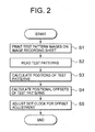
- the writing unit circuit section 200 At the time of offset detection, the writing unit circuit section 200 generates images with predetermined patterns stored in a ROM 221 at a total of three or more positions, i.e., the start position, end position, and intermediate position on the photosensitive drum 10 in the main scanning direction (S1 in Fig. 2).
- Fig. 3 shows a case wherein patterns in the form of the Katakana character " " are printed as predetermined patterns at three positions in the main scanning direction.
- a distance Y1' from the horizontal line to the oblique line of the pattern in the form of the Katakana character " " includes an offset dy1, and distances Y2' and Y3' respectively include offsets dy2 and dy3.
- the offset dy1 can also be obtained from the moving speed of the image carrier in the sub-scanning direction and the difference between the times when the horizontal and oblique lines are read.
- dx2 dy2/tané.
- the offset dy2 can be obtained from the moving speed of the image carrier in the sub-scanning direction and the difference between times when the horizontal and oblique line are read.
- dx3 dy3/tané.
- the offset dy3 can be obtained from the moving speed of the image carrier in the sub-scanning direction and the difference between times when the horizontal and oblique line are read.
- the positions (offset states) of the test patterns are calculated by the CPU 201 (S3 in Fig. 2).
- the CPU 201 compares the positions (offset states) of the test patterns with the reference distances based on the test patterns to calculate pixel offset states within the image recording sheet surface (S4 in Fig. 2).
- the CPU 201 can detect offset states (frequency offset information) associated with the expansion/contraction of an image and pixel offsets in the main scanning direction.
- the CPU 201 performs the above detection processing with respect to one surface of the image recording sheet in this manner, and supplies frequency offset information ( in Fig. 1) to the selection control section 215 of the writing unit circuit section 200.
- the CPU 201 can obtain image leading end offset information associated with the start position of an image in the main scanning direction by detecting the pattern in the form of the Katakana character " " on the start end side in the main scanning direction, and can supply the image leading end offset information to the selection control section 215 in the writing unit circuit section 200.
- the dot clock adjusting section 210 in usual image printing operation, on the basis of frequency offset information representing a pixel offset state on one surface, the dot clock adjusting section 210 generates a dot clock for eliminating a halfway offset which is the pixel offset state on one surface of the image recording sheet, thereby printing an image (S5 in Fig. 2)
- the CPU 201 supplies a correction amount computing section in the selection control section 215 with offset information representing an offset ER detected by the above printing and reading of the predetermined patterns, clock frequency information of a clock period TC obtained from the frequency of a fundamental clock, one-line pixel count information representing a pixel count PH of pixels to be printed in the main scanning direction.
- a synchronization count (a count by which a delay of one fundamental clock period) NS is obtained from the first synchronization point information SP1 and second synchronization point information SP2 from the synchronization detecting section 214.
- This correction count value CC is counted down by a switching count device in the selection control section 215 to switch between a select signal and a low-order select signal. As the correction amount increases, therefore, the correction count value CC decreases.
- the synchronization detecting section 214 refers to the leading edge of an index signal from the index sensor 266 to obtain, as synchronization point information, the ordinal number of a delay element of the delay chain section 213 at which a delay signal synchronized with the leading edge of the index signal is obtained.
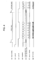
- an index signal is generated at the timing when the index sensor detects a laser beam scanned by the writing unit (T1 of (a) in Fig. 4). Thereafter, H_VALID representing a valid area in the horizontal direction is activated.
- the switching count device in the selection control section 215 keeps counting down the correction count value CC in accordance with a fundamental clock. Every time the count values is counted down to 0, count data is supplied as an interrupt to a select signal computing section 443 in the selection control section 215 ((d) to (f) in Fig. 4).
- the CPU 201 supplies offset direction information to the select signal computing section in the selection control section 215. More specifically, the CPU 201 supplies "-correction" information for making correction to contract an offset as image expansion in the main scanning direction, and "+correction” information for making correction to expand an offset as image contraction.
- offset information ER and offset direction information have been obtained by printing and measuring the predetermined patterns described above.
- ER 6 ns
- offset direction information "-correction". That is, assume that the obtained information indicates making correction to contract the image because of its expansion.
- the synchronization detecting section 214 obtains the first synchronization point information SP1 and second synchronization point information SP2 by referring to the leading edge of an index signal from the index sensor 266.
- the first synchronization point information SP1 indicates the ordinal number of a delay element of the delay chain section 213 which is synchronized with the leading edge of the index signal.
- the second synchronization point information SP2 indicates the ordinal number of a delay element of the delay chain section 213 which lags behind the first synchronization point information SP1 by one fundamental clock period.
- Fig. 5 shows this state.
- 20th DL 20 ((c) in Fig. 5) and 50th DL 50 ((m) in Fig. 5) lagging behind DL 20 by one clock period are synchronized with the leading edge of the index signal ((a) in Fig. 5).
- the synchronization count NS is then obtained from the first synchronization point information SP1 and second synchronization point information SP2.
- the synchronization count NS indicates a specific number of delay elements to which a time of one fundamental clock period corresponds in terms of delay time.
- a delay time DT of per delay element is obtained from NS and the fundamental clock period.
- a fundamental clock period TC is 30 ns.
- the delay time per delay element varies due to variations in the temperature of an integrated circuit, the power supply voltage applied to the integrated circuit, and the like, and hence may become 1.5 ns in some case and 0.5 ns in another case.
- the fundamental clock period TC is constant, the delay time per delay element at the time of measurement can be accurately obtained by obtaining the synchronization count NS.
- correction count value CC indicating how many delay elements by which a shift should be finally made to obtain a proper image signal is obtained from the offset information ER, offset direction information, and delay time DT.
- ER 6 ns
- offset direction information "-correction”
- the delay element count may be finally advanced by six. That is, a signal from the 50th delay element is used in synchronism with the leading edge of an index signal, and signals from the 49th, 48th, 47th, 46th, and 45th delay elements are sequentially interchanged and used in synchronism with a select signal. Finally, a signal from the 44th delay element is used.
- a select signal may be circulated.
- a select signal may be circulated in the same manner.
- the selecting section 216 selects the 50th signal, 49th signal, 48th signal, 47th signal, ... from a delay signal group ( in Fig. 1) from the delay chain section 213, and outputs them as dot clocks ((g) in Fig. 4).
- adjustment can be made to set the pulse count to a predetermined count by shifting the pulse of a fundamental clock at given time intervals and to set the time during which the predetermined number of pulses are generated to a predetermined time.
- Fig. 6 schematically shows how the above correction of expansion/contraction in the main scanning direction (i.e., main-scanning magnification correction) is made.
- Fig. 6 shows a fundamental clock, delay signals (first to ninth delay clocks), and a dot clock.
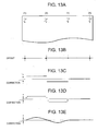
- Figs. 13A to 13E show a case wherein test patterns are printed at four different positions in the main scanning direction ( to in Fig. 13A).
- the interval between (1) and (2) has decreased. Since no halfway offset has occurred at (3), the interval between (2) and (3) has increased. In addition, since no halfway offset has occurred at (4), the length in the main scanning direction is assumed to be a predetermined length.
- the CPU 201 When the above halfway offset has occurred, the CPU 201 performs control to increase the interval between dot clocks between (1) and (2) by the above "+ correction". Likewise, the CPU 201 performs control to decrease the interval between dot clocks between (2) and (3) by the above "- correction". Since no change in interval has occurred between (3) and (4), no correction is performed. With the above operation, the halfway offset can be eliminated, and a state wherein there is no change in length in the main scanning direction can be obtained.
- Figs. 13A to 13E show an example of a halfway offset, which can be eliminated to make the main-scanning length constant by applying this embodiment and performing proper correction in accordance with the halfway offset.
- the use of the digital delay type dot clock adjusting section in the above manner can adjust an offset between the start and the end in the main scanning direction.
- a halfway offset can be suppressed by adjusting the timing of a dot clock at three or more positions in the main scanning direction using pieces of error information at three or more positions on one surface of an image recording sheet in the main scanning direction.
- not only expansion/contraction between the start and the end but also a pixel offset caused at a halfway point (halfway offset) may pose a serious problem.
- satisfactory offset correction can be performed by this embodiment of the present invention.
- test patterns at the three positions.
- increasing the number of test patterns will suppress halfway offsets more finely. If, for example, test patterns are printed at four positions, halfway offset suppression can be done in areas on the left end portion/near the center/on the right end portion. That is, offset correction can be done at three positions by using test patterns at four positions, thereby obtaining a better result.
- the first embodiment uses the digital circuit arrangement having no analog feedback circuit such as a PLL. This circuit and other digital circuit portions can therefore be integrated into one chip. This makes it possible to perform halfway offset elimination with higher precision.
- L be the number of pixels per line in the main scanning direction, which are used for image printing
- L1 to Ln-1 be the numbers of pixels in the respective ranges divided by n test patterns (n is equal to or more than 3)
- N1 to Nn-1 be the offset amounts calculated between the three or more test patterns
- an offset correction amount Nj/Lj (where 1 j n) between each pair of test patterns be evenly distributed to the respective pixels between each pair of test patterns so as to be reflected in the selection of a delay count for a dot clock.
- error information is detected at three or more positions in the main scanning direction and is evenly distributed to the respective pixels between each pair of test patterns so as to be reflected in the selection of a delay count for a dot clock.
- This can align the starts and the ends of the respective lines and properly suppress a halfway offset as a pixel offset in a halfway portion.
- the CPU 201 is externally provided for the dot clock adjusting section 210.
- the dot clock adjusting section 210 may incorporate controllers such as the CPU 201 and various kinds of tables.
- a dot clock as the basis of each pixel forming an image is generated and exposure of each pixel is to be performed on one surface of an image recording sheet on the basis of the dot clock
- a plurality of delay clocks are generated by finely delaying a fundamental clock, and the manner of selection for the plurality of delay clocks is changed to change the leading edge timing or trailing edge timing of the dot clock generated for a surface on which an offset should be adjusted.
- test patterns are printed at three or more positions on an image printing surface in the main scanning direction to detect error information associated with an offset on one surface, and the manner of selection of a plurality of delay clocks is controlled in accordance with the error information, thereby correcting an offset on one surface.
- this embodiment uses the digital circuit arrangement having no analog feedback circuit such as a PLL, the circuit and other digital circuit portions can be integrated into one chip. This makes it possible to perform halfway offset elimination with higher precision.
- offset correction is executed upon detection of error information at three or more positions in the main scanning direction. This can align the starts and the ends of the respective lines in the main scanning direction and adjust a halfway offset as a pixel offset in a halfway portion between the start and the end of each line.
- the offset detecting section, digital delay type dot clock adjusting device, and controller can be formed from digital circuits. These sections can perform halfway offset elimination with high precision in a state wherein they are suitable for integration into one chip.
- the first embodiment described above is directed to halfway offset correction. If, however, a pattern in the form of the Katakana character " " to be printed on the start side in the main scanning direction is placed as near the end portion at the start position in the main scanning direction as possible, and image leading end offset information associated with the start position of an image in the main scanning direction is supplied to the selection control section 215 in the writing unit circuit section 200, the start positions of the respective lines in the main scanning direction can be aligned.
- a halfway offset is detected by the halfway offset sensor 270a, and an offset is set.
- the CPU 201 may analyze the image data obtained by making a scanner (not shown) read an image recording sheet on which test patterns are printed, and set an offset.
- an operator may measure an image recording sheet on which test patterns are printed, and set an offset obtained from the measurement result with respect to the CPU 201 with an operating section (not shown).
- the image printing apparatus shown in Figs. 14 and 7 is assumed to be a specific example of an image printing apparatus according to the second embodiment. That is, the image printing apparatus according to the second embodiment is an image printing apparatus capable of printing images on the two surfaces of an image recording sheet. Note that this apparatus may either be a monochrome image printing apparatus or color image printing apparatus.
- Fig. 8 shows a writing unit circuit section 200, an LD 260 for performing exposure, an index sensor 266, and an obverse/reverse pixel offset sensor 270b.
- the writing unit circuit section 200 of a writing unit 20 forms an electrostatic latent image by scanning a laser beam on the surface of a photosensitive drum 10 (see Fig. 7) in accordance with image data.
- the writing unit circuit section 200 includes a CPU 201 serving as a controller for controlling the overall image printing apparatus, a dot clock adjusting section 210 which is a characteristic feature of the second embodiment, an image processing section 220 for performing image processing, and an LD driving section 230 for generating an LD driving signal in accordance with a dot clock based on the image processing result.
- a CPU 201 serving as a controller for controlling the overall image printing apparatus
- a dot clock adjusting section 210 which is a characteristic feature of the second embodiment
- an image processing section 220 for performing image processing
- an LD driving section 230 for generating an LD driving signal in accordance with a dot clock based on the image processing result.
- the obverse/reverse pixel offset sensor 270b is placed downstream of a fixing unit 70 to detect pixel offsets at three or more positions in the main scanning direction and read predetermined patterns after fixing.
- the predetermined pattern means a test image printed in accordance with test image data stored in advance.
- the dot clock adjusting section 210 is a clock generating section in the claims.
- the dot clock adjusting section 210 is comprised of a clock generating section 211 for generating a fundamental clock and a frequency changing section 212 capable of changing the frequency of the fundamental clock generated by the clock generating section 211.
- the frequency changing section 212 changes the leading or trailing edge timing or frequency of a dot clock to a desired timing such as a given timing during scanning of one line or a timing corresponding to each image printing surface or image printing color in order to change the position of a pixel printed in accordance with the dot clock.
- the frequency changing section 212 is formed from a digital delay type dot clock adjusting device, and is comprised of (A), (B), (C), and (D) described below.
- a delay chain section 213 is a delay element group for obtaining a plurality of delay signals (delay signal group: in Fig. 8) having slightly different phases from each other by delaying an input signal (the fundamental clock from the clock generating section 211).
- delay elements are preferably cascaded in the form of a chain to connect a sufficient number of delay elements to generate delay signals having slightly different phases from each other over two fundamental clock periods.
- clock generating section 211 may be incorporated in each of clock generating circuits for the respective colors, i.e., Y, M, C, and K in a case of a color image printing apparatus, fundamental clocks may be distributed from the single clock generating section 211 to the clock generating circuits for the respective colors.
- the index sensor 266 detects an exposure timing at a reference position in scanning of a laser beam, and generates an index signal indicating the timing.
- a synchronization detecting section 214 is a detecting section which receives the index signal generated by the index sensor 266 and detects the ordinal number of a delay signal' (synchronization point), of a delay signal group ( in Fig. 8), which is synchronized with the index signal. This section outputs synchronization point information ( in Fig. 8).
- the synchronization detecting section 214 preferably outputs first synchronization point information SP1 indicating a delay signal, of the delay signal group ( in Fig. 8), which is synchronized first with the index signal, and second synchronization point information SP2 indicating a delay signal synchronized next with the index signal.
- a plurality of delay signals from the delay chain section 213 may greatly vary in delay time due to the influences of temperature changes and the like, how many delay signals are included in a predetermined unchanging time (the time interval between an index signal and another index signal) is detected in advance in this manner. This makes it possible to calculate back the delay time per delay signal of a delay signal group.
- a selection control section 215 obtains a synchronization correction amount on the basis of synchronization point information ( in Fig. 8) from the synchronization detecting section 214 and frequency offset information ( in Fig. 8) from the CPU 201, and outputs a select signal ( in Fig. 8) indicating a delay signal having a specific phase which is to be selected from a delay signal group ( in Fig. 8).
- the frequency offset information will be described later.
- a selecting section 216 receives a select signal ( in Fig. 8) from the selection control section 215, and selects a delay signal having a corresponding phase from a delay signal group ( in Fig. 8). The selecting section 216 then generates a rectangular wave by setting the selected delay signal as leading and trailing edges, and outputs the rectangular wave as a dot clock ( in Fig. 8).
- the period of a dot clock is slightly increased or decreased by setting a delay signal having a selected timing as leading and trailing edges in generating a dot clock. This can realize (a) and (b) described below.
- the writing unit circuit section 200 generates images with predetermined patterns stored in a ROM 221 at a total of three or more positions, i.e., the start position, end position, and intermediate position on the photosensitive drum 10 in the main scanning direction (S1 in Fig. 9).
- Fig. 3 shows a case wherein patterns in the form of the Katakana character " 7 " are printed as predetermined patterns at three positions in the main scanning direction.
- a distance Y1' from the horizontal line to the oblique line of the pattern in the form of the Katakana character " " includes an offset dy1, and distances Y2' and Y3' respectively include offsets dy2 and dy3.
- the offset dy1 can also be obtained from the moving speed of the image carrier in the sub-scanning direction and the difference between the times when the horizontal and oblique lines are read.
- dx2 dy2/tané.
- the offset dy2 can be obtained from the moving speed of the image carrier in the sub-scanning direction and the difference between times when the horizontal and oblique line are read.
- dx3 dy3/tané.
- the offset dy3 can be obtained from the moving speed of the image carrier in the sub-scanning direction and the difference between times when the horizontal and oblique line are read.
- the positions of the test patterns are calculated by the CPU 201 (S3 in Fig. 9).
- the image recording sheet whose test patterns printed on one surface are read is caused to pass along a reversal convey path to also print test patterns on the other surface in the same manner (S4 in Fig. 9).
- the obverse/reverse pixel offset sensor 270b reads the test patterns (S5 in Fig. 9).
- the positions of the test patters (offset states) are then calculated (S6 in Fig. 9).
- the CPU 201 calculates pixel offset states on the two surfaces by comparing the positions (offset states) of the test patterns on the respective surfaces (S7 in Fig. 9).
- the CPU 201 may calculate pixel offset states on the respective surfaces by comparing the positions (offset states) of the test patterns on the respective surfaces with the reference distances based on the test patterns.
- the CPU 201 can detect offset states (frequency offset information) associated with the expansion/contraction of an image and pixel offsets in the main scanning direction.
- the CPU 201 performs the above detection processing with respect to the two surfaces of the image recording sheet in this manner, and supplies frequency offset information ( in Fig. 8) to the selection control section 215 of the writing unit circuit section 200.
- the CPU 201 can obtain image leading end offset information associated with the start position of an image in the main scanning direction by detecting the pattern in the form of the Katakana character "7" on the start end side in the main scanning direction, and can supply the image leading end offset information to the selection control section 215 in the writing unit circuit section 200.
- the dot clock adjusting section 210 in usual image printing operation, on the basis of frequency offset information representing pixel offset states on the two surfaces, the dot clock adjusting section 210 generates dot clocks for eliminating the pixel offset states on the two surfaces of the image recording sheet, thereby printing an image (S8 in Fig. 9)
- the use of the digital delay type dot clock adjusting section in the above manner can adjust an offset between the start and the end in the main scanning direction.
- An obverse/reverse pixel offset can be suppressed by adjusting the timing of a dot clock at three or more positions in the main scanning direction using pieces of error information at three or more positions on each of the obverse and reverse surfaces of an image recording sheet in the main scanning direction.
- test patterns at the three positions.
- increasing the number of test patterns will suppress obverse/reverse pixel offsets more finely. If, for example, test patterns are printed at four positions, obverse/reverse pixel offset suppression can be done in areas on the left end portion/near the center/on the right end portion. That is, offset correction can be done at three positions by using test patterns at four positions, thereby obtaining a better result.
- the second embodiment uses the digital circuit arrangement having no analog feedback circuit such as a PLL.
- This circuit and other digital circuit portions can therefore be integrated into one chip. This makes it possible to perform obverse/reverse pixel offset elimination with higher precision.
- L be the number of pixels per line in the main scanning direction which are used for image printing
- L1 to Ln-1 be the numbers of pixels in the respective ranges divided by n test patterns (n is equal to or more than 3)
- N1 to Nn-1 be the offset amounts calculated between the three or more test patterns
- an offset correction amount Nj/Lj (where 1 j n) between each pair of test patterns be evenly distributed to the respective pixels between each pair of test patterns so as to be reflected in the selection of a delay count for a dot clock.
- error information is detected at three or more positions in the main scanning direction and is evenly distributed to the respective pixels between each pair of test patterns so as to be reflected in the selection of a delay count for a dot clock. This can align the starts and the ends of the respective lines and properly perform pixel offset adjustment in a halfway portion.
- the CPU 201 is externally provided for the dot clock adjusting section 210.
- the dot clock adjusting section 210 may incorporate controllers such as the CPU 201 and various kinds of tables.
- a dot clock as the basis of each pixel forming an image is generated and exposure of each pixel is to be performed on the two surfaces of an image recording sheet on the basis of the dot clock
- a plurality of delay clocks are generated by finely delaying a fundamental clock, and the manner of selection for the plurality of delay clocks is changed to change the leading edge timing or trailing edge timing of the dot clock generated for a surface on which an offset should be adjusted.
- test patterns are printed at three or more positions on each surface in the main scanning direction to detect error information associated with an offset on each surface, and the manner of selection of a plurality of delay clocks is controlled in accordance with the error information, thereby correcting an offset on one surface.
- this embodiment uses the digital circuit arrangement having no analog feedback circuit such as a PLL, the circuit and other digital circuit portions can be integrated into one chip. This makes it possible to perform halfway offset elimination with higher precision.
- offset correction is executed upon detection of error information at three or more positions in the main scanning direction. This can align the starts and the ends of the respective lines in the main scanning direction and adjust an obverse/reverse pixel offset as a pixel offset in a halfway portion between the start and the end of each line.
- the second embodiment has the digital delay type dot clock adjusting device as a circuit common to the respective surfaces on which offsets should be adjusted. This makes it possible to reduce the circuit size while eliminating an obverse/reverse pixel offset with high precision.
- the digital delay type dot clock adjusting device and controller can be formed from digital circuits. These sections can perform obverse/reverse pixel offset elimination with high precision in a state wherein they are suitable for integration into one chip.
- the apparatus since the apparatus operates under the control of a controller such as a CPU externally provided for the digital delay type dot clock adjusting device, an obverse/reverse pixel offset can be eliminated with high precision.
- the apparatus since the apparatus operates under the control of a controller such as a CPU incorporated in the digital delay type dot clock adjusting device, obverse/reverse pixel offset elimination can be done with high precision in a state wherein the device is suitable for integration into one chip.
- a controller such as a CPU incorporated in the digital delay type dot clock adjusting device
- the second embodiment described above is directed to obverse/reverse pixel offset correction. If, however, a pattern in the form of the Katakana character " " to be printed on the start side in the main scanning direction is placed as near the end portion at the start position in the main scanning direction as possible, and image leading end offset information associated with the start position of an image in the main scanning direction is supplied to the selection control section 215 in the writing unit circuit section 200, the start positions of the respective lines in the main scanning direction can be aligned.
- an obverse/reverse pixel offset is detected by the obverse/reverse pixel offset sensor 270b, and an offset is set.
- the CPU 201 may analyze the image data obtained by making a scanner (not shown) read an image recording sheet on which test patterns are printed, and set an offset.
- an operator may measure an image recording sheet on which test patterns are printed, and set an offset obtained from the measurement result with respect to the CPU 201 with an operating section (not shown).
- the third embodiment of the present invention will be described below.
- the third embodiment is directed to a color image printing apparatus having an exposure unit (see Fig. 14) for each of a plurality of colors to print an image in a plurality of colors.
- This color image printing apparatus scans a laser beam modulated in accordance with image data in the main scanning direction for each color, and forms an image in each color on an image carrier for each color which rotates in the sub-scanning direction.
- the laser beam is modulated with the image data with reference to a pixel clock called a dot clock.
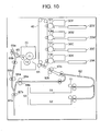
- Fig. 10 is a sectional view showing the arrangement of the print engine of the image printing apparatus according to the third embodiment.
- Fig. 10 shows a specific example of the image printing apparatus which can print a color image by using toners of a plurality of colors.
- toner image from the image carriers of the respective colors are primarily transferred to the intermediate transfer member and superimposed thereon.
- An image recording sheet is then clamped between the intermediate transfer member and the transfer roller to secondarily transfer the image from the intermediate transfer member to the image recording sheet, thereby printing the image.
- Reference numeral 10Y to 10K denote photosensitive drums serving as image carriers on which Y (Yellow), M (Magenta), C (Cyan), and K (blacK) toner images are formed.
- Reference numerals 20Y to 20K denote writing units for forming electrostatic latent images on the surfaces of the photosensitive drums 10Y to 10K by scanning laser beams in accordance with pieces of image information of the respective colors.
- Reference numerals 30Y to 30K denote developing devices for forming toner images by developing the electrostatic latent images formed on the surfaces of the photosensitive drums 10Y to 10K with developers (toners) o the respective colors.
- Reference numeral 40 denotes an intermediate transfer member belt on which the toner images from the photosensitive drums 10Y to 10K of the respective colors are transferred (primarily transferred) and superimposed; and 64, a secondary transfer roller for transferring (secondarily transferring) the toner image from the intermediate transfer member belt 40 onto an image recording sheet, and separating the image recording sheet from the intermediate transfer member belt 40. Note that an illustration of a belt cleaning section and the like is omitted.
- Reference numeral 50 denotes a paper feed section in which image recording sheets are stored.
- Fig. 10 shows paper feed cassettes 51 and 52 of the paper feed section 50. Note that the number of paper feed cassettes is not limited to this.
- Reference numerals 61 to 68 denote convey devices such as convey rollers and path switching device.
- Reference numeral 61 denotes a feed roller for feeding an image recording sheet from a paper feed cassette; 62, a convey path along which an image recording sheet from the paper feed section 50 (51 or 52) travels; 63a and 63b, registration rollers for feeding an image recording sheet at the timing of image printing; 64, a secondary transfer roller; 65, a path switching device which switches between delivery and circulation of an image recording sheet; 66a, 66b, 67a, 67b, 68a, and 68b, inversion rollers for inverting the obverse and reverse surfaces of an image recording sheet; and 69a and 69b, delivery rollers for delivering an image recording sheet outside the apparatus.
- Reference numeral 70 denotes a fixing unit for fixing a toner image on an image recording sheet with heat and pressure.
- the fixing unit 70 has a heat roller 71 (or 72) and a pressure roller 72 (or 71).
- the arrangement of a writing unit using a laser beam in this manner is the same as that shown in Fig. 14 which has already been described in the first embodiment.
- the writing units 20Y, 20M, 20C, and 20K also have the same arrangement.
- the image printing apparatus according to the third embodiment is an image printing apparatus capable of printing images in a plurality of colors, i.e., at least two colors.
- This embodiment will exemplify a color image printing apparatus using toners of four colors, i.e., Y (Yellow), M (Magenta), C (Cyan), and K (blacK).
- Fig. 11 shows a CPU 201 serving as a controller for controlling the overall image printing apparatus, a writing unit circuit section 200Y for Y, a writing unit circuit section 200M for M, a writing unit circuit section 200C for C, a writing unit circuit section 200K for K, an LD 260Y for performing exposure for Y, an LD 260M for performing exposure for M, an LD 260C for performing exposure for C, an LD 260K for performing exposure for K, an index sensor 266Y for Y, an index sensor 266M for M, an index sensor 266C for C, and an index sensor 266K for K.
- the writing unit circuit sections 200Y to 200K are circuit sections for the writing units 20Y to 20K for forming electrostatic latent images on the surfaces of the photosensitive drums 10Y to 10K by scanning laser beams in accordance with pieces of image information of the respective colors.
- FIG. 11 shows the detailed arrangement of the writing unit circuit section 200Y, the remaining writing unit circuit sections 200M, 200C, and 200K have the same arrangement.
- the writing unit circuit section 200Y has a dot clock adjusting section 210 which is a characteristic feature of the third embodiment, an image processing section 220 for performing image processing, and an LD driving section 230 for generating an LD driving signal in accordance with a dot clock on the basis of an image processing result.
- a color misregistration sensor 270c is placed to detect pixel offsets at three or more positions in the main scanning direction and read predetermined test patterns of the respective color after fixing.
- the dot clock adjusting section 210 is a clock generating section in the claims.
- the dot clock adjusting section 210 is comprised of a clock generating section 211 for generating a fundamental clock and a frequency changing section 212 capable of changing the frequency of the fundamental clock generated by the clock generating section 211.
- the frequency changing section 212 changes the leading or trailing edge timing or frequency of a dot clock to a desired timing such as a given timing during scanning of one line or a timing corresponding to each image printing surface or image printing color in order to change the position of a pixel printed in accordance with the dot clock.
- the frequency changing section 212 is formed from a digital delay type dot clock adjusting device, and is comprised of (A), (B), (C), and (D) described below.
- a delay chain section 213 is a delay element group for obtaining a plurality of delay signals (delay signal group: in Fig. 11) having slightly different phases from each other by delaying an input signal (the fundamental clock from the clock generating section 211).
- delay elements are preferably cascaded in the form of a chain to connect a sufficient number of delay elements to generate delay signals having slightly different phases from each other over two fundamental clock periods.
- clock generating section 211 may be incorporated in each of clock generating circuits for the respective colors, i.e., Y, M, C, and K, fundamental clocks may be distributed from the single clock generating section 211 to the clock generating circuits for the respective colors.
- the index sensor 266Y detects a reference position in scanning of a laser beam.
- a synchronization detecting section 214 is a detecting section which receives the index signal generated by the index sensor 266Y and detects the ordinal number of a delay signal (synchronization point), of a delay signal group ( in Fig. 11), which is synchronized with the index signal. This section outputs synchronization point information ( in Fig. 11).
- the synchronization detecting section 214 preferably outputs first synchronization point information SP1 indicating a delay signal, of the delay signal group ( in Fig. 11), which is synchronized first with the index signal, and second synchronization point information SP2 indicating a delay signal synchronized next with the index signal.
- a plurality of delay signals from the delay chain section 213 may greatly vary in delay time due to the influences of temperature changes and the like, how many delay signals are included in a predetermined unchanging time (the time interval between an index signal and another index signal) is detected in advance in this manner.
- a selection control section 215 obtains a synchronization correction amount on the basis of synchronization point information ( in Fig. 11) from the synchronization detecting section 214 and frequency offset information ( in Fig. 11) from the CPU 201, and outputs a select signal ( in Fig. 11) indicating a delay signal having a specific phase which is to be selected from a delay signal group ( in Fig. 11).
- the frequency offset information will be described later.
- a selecting section 216 receives a select signal ( in Fig. 11) from the selection control section 215, and selects a delay signal having a corresponding phase from a delay signal group ( in Fig. 11). The selecting section. 216 then generates a rectangular wave by setting the selected delay signal as leading and trailing edges, and outputs the rectangular wave as a dot clock ( in Fig. 11).
- the period of a dot clock is slightly increased or decreased by setting a delay signal having a selected timing as leading and trailing edges in generating a dot clock, thereby generating a signal whose pulse count representing the number of pulses generated within a predetermined period of time is set to a predetermined count.
- the pulse count within the predetermined period of time is set to the predetermined count by sequentially selecting delay signals, whose phases (the positions or timings of the pulses of a dot clock) are finely and gradually changed, within a predetermined period of time without changing the clock frequency itself instead of making adjustment by finely adjusting the oscillation frequency of a fundamental clock oscillated and generated by the clock generating section 211.
- the period of a dot clock is slightly increased or decreased by setting a delay signal having a selected timing as leading and trailing edges in generating a dot clock. This can realize (a) and (b) described below.
- the writing unit circuit section 200 At the time of offset detection, the writing unit circuit section 200 generates images with predetermined patterns stored in a ROM 221 at a total of three or more positions, i.e., the start position, end position, and intermediate position on the intermediate transfer member belt 40 in the main scanning direction (S1 in Fig. 12).
- Fig. 3 shows a case wherein patterns in the form of the Katakana character " " are printed as predetermined patterns at three positions in the main scanning direction.
- offsets dx1, dx2, and dx3 have occurred in the main scanning direction due to the aberrations of the writing unit and the respective optical systems and the like.
- a distance Y1' from the horizontal line to the oblique line of the pattern in the form of the Katakana character " " includes an offset dy1, and distances Y2' and Y3' respectively include offsets dy2 and dy3.
- the offset dy1 can also be obtained from the moving speed of the image carrier in the sub-scanning direction and the difference between the times when the horizontal and oblique lines are read.
- dx2 dy2/tané.
- the offset dy2 can be obtained from the moving speed of the image carrier in the sub-scanning direction and the difference between times when the horizontal and oblique line are read.
- dx3 dy3/tané.
- the offset dy3 can be obtained from the moving speed of the image carrier in the sub-scanning direction and the difference between times when the horizontal and oblique line are read.
- the positions of the test patterns are calculated by the CPU 201 (S3 in Fig. 12).
- test patterns are printed (S4 in Fig. 12), the test patterns are read by the color misregistration sensor 270c (S5 in Fig. 12), and the positions (offset states) of the test patters are calculated (S6 in Fig. 12).
- the CPU 201 compares the positions (offset states) of the test patterns in the respective colors to calculate pixel offset states for the respective colors (S7 in Fig. 12).
- the CPU 201 may calculate pixel offset states for the respective colors by comparing the positions (offset states) of the test patters of the respective colors with the reference distances based on the test patterns.
- the CPU 201 can detect offset states (frequency offset information) associated with the expansion/contraction of an image in the main scanning direction and pixel offsets in an intermediate portion.
- the CPU 201 performs the above detection processing for the respective colors in this manner, and supplies frequency offset information ( in Fig. 11) to the writing units 20Y to 20K.
- the CPU 201 can obtain image leading end offset information associated with the start position of an image in the main scanning direction by detecting the pattern in the form of the Katakana character " " on the start end side in the main scanning direction, and can supply the image leading end offset information to the writing unit.
- the dot clock adjusting section 210 in usual image printing operation, on the basis of frequency offset information representing pixel offset states for the respective colors, the dot clock adjusting section 210 generates dot clocks for eliminating the pixel offset states for the respective colors, thereby printing an image (S8 in Fig. 12)
- offsets in the main scanning direction can be adjusted by using the digital delay type dot clock adjusting device.
- Setting the length of one main-scanning line of one of Y, M, C, and K as a reference length and matching the length of one main-scanning line of each of the remaining colors with the reference length to align the leading end positions of the respective lines can suppress color misregistration in printing a color image.
- the leading end position and length of one line of a given color in the main scanning direction are measured by the technique shown in Fig. 3, and the dot clock adjusting section is so operated as to match the leading positions and lengths of lines of the remaining colors in the main scanning direction with those of the line of the given color. This allows the images of the respective colors to coincide with each other, thus eliminating color misregistration in the main scanning direction which is caused by various factors.
- the use of the digital delay type dot clock adjusting section in the above manner can adjust an offset between the start and the end in the main scanning direction.
- a pixel offset for each color can be suppressed by adjusting the timing of a dot clock at three or more positions in the main scanning direction using pieces of error information at three or more positions in the main scanning direction for each color.
- test patterns at the three positions.
- increasing the number of test patterns will suppress obverse/reverse pixel offsets more finely. If, for example, test patterns are printed at four positions, obverse/reverse pixel offset suppression can be done in areas on the left end portion/near the center/on the right end portion. That is, offset correction can be done at three positions by using test patterns at four positions, thereby obtaining a better result.
- This embodiment uses the digital circuit arrangement having no analog feedback circuit such as a PLL.
- This circuit and other digital circuit portions can therefore be integrated into one chip. This makes it possible to perform obverse/reverse pixel offset elimination with higher precision.
- L be the number of pixels per line in the main scanning direction which are used for image printing
- L1 to Ln-1 be the numbers of pixels in the respective ranges divided by n test patterns (n is equal to or more than 3)
- N1 to Nn-1 be the offset amounts calculated between the three or more test patterns
- an offset correction amount Nj/Lj (where 1 j n) between each pair of test patterns be evenly distributed to the respective pixels between each pair of test patterns so as to be reflected in the selection of a delay count for a dot clock.
- error information is detected at three or more positions in the main scanning direction and is evenly distributed to the respective pixels between each pair of test patterns so as to be reflected in the selection of a delay count for a dot clock. This can align the starts and the ends of the respective lines and properly perform pixel offset adjustment in a halfway portion.
- the CPU 201 is externally provided for the dot clock adjusting section.
- the dot clock adjusting section may incorporate controllers such as CPU and tables.
- a dot clock is generated for each of a plurality of colors used to print an image, and exposure for each color is to be performed on the basis of the dot clock
- a plurality of delay clocks are generated by finely delaying a fundamental clock, and the manner of selection for the plurality of delay clocks is changed to change the leading edge timing or trailing edge timing of the dot clock generated for a color for which an offset should be adjusted.
- an image printed in a given color (or the desired value of image data of a test pattern) is set as a reference, and test patterns are printed at three or more positions in the main scanning direction with respect to image offsets of the remaining colors, thereby detecting error information associated with color misregistration.
- the selection of a plurality of delay clocks in the above digital delay type dot clock adjusting device is controlled on the basis of the error information, thereby correcting the offset. Since this embodiment uses the digital circuit arrangement having no analog feedback circuit such as a PLL, the circuit and other digital circuit portions can be integrated into one chip. This makes it possible to perform color misregistration elimination with higher precision.
- offset correction is executed upon detection of error information at three or more positions in the main scanning direction. This can align the starts and the ends of the respective lines and adjust a pixel offset in an intermediate portion.
- the delay chain section generates a plurality of delay clocks by finely delaying a fundamental clock
- the synchronization detecting section detects synchronization information.
- the selection control section then generates a select signal from the synchronization information and error information.
- the selecting section selects a delay clock corresponding to the select signal from a plurality of delay signals and outputs it as a dot clock. Since the digital delay type dot clock adjusting device has a digital circuit arrangement having no analog feedback circuit such as a PLL, the circuit and other digital circuit portions can be integrated into one chip. This makes it possible to perform high-precision color misregistration elimination.
- the third embodiment includes digital delay type dot clock adjusting devices as independent circuits for the respective colors for which color misregistration should be performed. This makes it possible to perform high-precision color misregistration elimination.
- the offset detecting section, digital delay type dot clock adjusting device, and controller are formed from digital circuits. These sections can perform color misregistration elimination with high precision in a state wherein they are suitable for integration into one chip.
- the image printing apparatus since the image printing apparatus operates under the control of a controller such as a CPU externally provided for the digital delay type dot clock adjusting device, color misregistration elimination can be performed with high precision.
- the image printing apparatus operates under the control of a controller such as a CPU incorporated in the digital delay type dot clock adjusting device, color misregistration elimination can be done with high precision by the digital delay type dot clock adjusting device in a state wherein the device is suitable for integration into one chip.
- the third embodiment described above is directed to color misregistration correction. If, however, a pattern in the form of the Katakana character " " to be printed on the start side in the main scanning direction is placed as near the end portion at the start position in the main scanning direction as possible, and image leading end offset information associated with the start position of an image in the main scanning direction is supplied to the selection control section 215 in the writing unit circuit section 200, the start positions of the respective lines in the main scanning direction can be aligned.
- color misregistration is detected by the color misregistration sensor 270c, and an offset is set.
- the CPU 201 may analyze the image data obtained by making a scanner (not shown) read an image recording sheet on which test patterns are printed, and set an offset.
- an operator may measure an image recording sheet on which test patterns are printed, and set an offset obtained from the measurement result with respect to the CPU 201 with an operating section (not shown).
- each embodiment of the present invention can be applied to various kinds of image forming apparatuses such as a laser imager for exposing a sheet of photographic paper to a laser beam and an inkjet printer which discharges ink from a head, and good results can be obtained.
Landscapes
- Engineering & Computer Science (AREA)
- Multimedia (AREA)
- Signal Processing (AREA)
- Laser Beam Printer (AREA)
- Control Or Security For Electrophotography (AREA)
- Facsimile Scanning Arrangements (AREA)
- Accessory Devices And Overall Control Thereof (AREA)
- Fax Reproducing Arrangements (AREA)
Abstract
This invention is directed to an image printing apparatus which can print images without any halfway offset or obverse/reverse pixel offset at a low cost. An image printing apparatus includes a clock generating section which generates a dot clock as the basis of each pixel forming an image, an image printing section which prints a one-line image in a main scanning direction in accordance with image data with reference to the dot clock output from the clock generating section, and prints a one-page image by repeating in the sub-scanning direction one-line image printing performed in the main scanning direction, and a clock control section which changeably controls the frequency of the dot clock during scanning of one line in the main scanning direction. <IMAGE>
Description
The present invention relates to an image printing
apparatus which prints a one-line image in the main
scanning direction in accordance with image data with
reference to a dot clock as the basis of each pixel forming
an image, and also prints a one-page image by repeating in
the sub-scanning direction one-line image printing
performed in the main scanning direction.
As an image printing apparatus, an apparatus for
printing a one-line image in the main scanning direction in
accordance with image data and printing a one-page image by
repeating in the sub-scanning direction one-line image
printing performed in the main scanning direction is known.
Image printing in the main scanning direction in
accordance with image data is performed with reference to a
clock signal (to be referred to as a "dot clock"
hereinafter in this specification) as the basis of each
pixel to be formed.
For example, in an electrophotographic image printing
apparatus, a laser beam modulated in accordance with image
data is scanned in the main scanning direction, and an
image is concurrently formed on an image carrier rotating
in the sub-scanning direction with the laser beam.
In this case, a laser beam is modulated with image
data with reference to a clock signal (pixel clock) called
a dot clock.
The arrangement of a writing unit as the main
component of an image printing apparatus using a laser beam
in this manner will be described with reference to Fig. 14.
In a writing unit circuit section 200, a laser diode
(LD) 260 emits a laser beam LB on the basis of a laser
driving signal LS generated on the basis of a dot clock.
The laser beam LB from the LD 260 passes through a
collimator lens 261 and cylindrical lens 262 and is then
scanned in the main scanning direction by a polygon mirror
263.
The laser beam LB scanned by the polygon mirror 263
is adjusted to be scanned at a constant velocity by an fè
lens 264. The laser beam further passes through a
cylindrical lens 265 to strike a photosensitive drum 10.
Sub-scanning operation is then performed by rotating
the photosensitive drum 10 during this main-scanning
operation. By repeating main-scanning operation in the
sub-scanning direction, a one-page image is printed.
Note that part of the laser beam LB scanned by the
polygon mirror is guided to an index sensor 266 to detect
the timing.
In an image printing apparatus designed to print a
one-page image by repeating such image printing operation,
performed in the main scanning direction, in the
sub-scanning direction, the main-scanning magnification
(the magnification in the main scanning direction) may
differ from a desired magnification due to the power
characteristics and mount precision of various kinds of
lens systems, the planarity and mount precision of various
kinds of mirrors, the planarity and mount precision of a
photosensitive drum as 'an image printing medium (image
carrier), individual differences thereof, and the like.
That is, an offset may occur in the main scanning direction.
An invention designed to change the frequency of a
dot clock to adjust such a main-scanning magnification
(eliminate an offset in the main scanning direction) is
disclosed in, for example, patent reference 1 below.
A plurality of writing units may be provided for the
above image printing apparatus to allow it to print a color
image. In this case, if offsets in the main scanning
direction occur between the respective writing units, a
proper color image cannot be printed.
In order to eliminate such offsets in the main
scanning direction, the frequency of a dot clock must be
changed for each color. Conventional techniques of this
type are disclosed in, for example, the following two
patent references:
Repeated studies by the present inventors show that
the following problems arise even though the main-scanning
magnification is adjusted to coincide with the desired
magnification by the techniques disclosed in the two patent
references described above.
Even if the distance between the start and the end in
the main scanning direction is made equal to a desired
distance, a halfway point, e.g., an intermediate point
between the start and the end, may not always coincide with
a desired position.
In other words, in some case, although the two ends,
i.e., the start and the end, coincide with desired
positions, a slight offset (halfway offset) may have
occurred between the two ends.
In the field of offset printing or the like, in
particular, not only expansion/contraction between the
start and the end but also a pixel offset at a halfway
point (halfway offset) may pose serious problems.
The factors that cause such halfway offsets include
the power characteristics and mount precision of various
kinds of lens systems, the planarity and mount precision of
various kinds of mirrors, the planarity and mount precision
of a photosensitive drum as an image printing medium (image
carrier), individual differences thereof, and the like. An
enormous cost is required to manufacture and mount these
components with high precision without causing any halfway
offset.
In printing a color image, if such halfway offsets
occur in different proportions among the respective colors,
the offsets appear as noticeable color misregistration,
posing a serious problem.
If the image printing apparatus is an image printing
apparatus capable of printing images on the two surfaces of
an image recording sheet, even if the distance between the
start and the end in the main scanning direction is
adjusted to a desired value, a user may recognize the
difference between the distances on the two surfaces as an
offset.
This is a case wherein an image recording sheet
having images printed on its obverse and reverse surfaces
is held up against light, an offset between the obverse and
reverse surfaces is recognized. Obviously, in this case, a
halfway offset may have occurred.
The present invention has been made to solve the
above problems in the prior art, and has as its object to
print images without any halfway offset or obverse/reverse
pixel offset at a low cost.
In order to achieve the above object, according to
the first aspect of the present invention, there is
provided an image printing apparatus comprising a clock
generating section which generates a dot clock as a basis
of each pixel forming an image, an image printing section
which prints a one-line image in a main scanning direction
in accordance with image data with reference to the dot
clock output from the clock generating section, and prints
a one-page image by repeating in the sub-scanning direction
one-line image printing performed in the main scanning
direction, and a clock control section which changeably
controls a frequency of the dot clock during scanning of
one line in the main scanning direction.
According the first aspect, when a one-line image is
printed in the main scanning direction in accordance with
image data with reference to a dot clock and a one-page
image is printed by repeating in the sub-scanning direction
one-line printing performed in the main scanning direction,
the frequency of the dot clock is changeably controlled
during scanning of one line in the main scanning direction.
According to the second aspect of the present
invention, there is provided an image printing apparatus,
wherein the clock control section described in the first
aspect controls even the number of pixels of one line in
the main scanning direction in a case in which the
frequency of the dot clock is changed during scanning of
one line to be equal to that in a case in which the
frequency is not changed.
According to the second aspect, even if the frequency
of the dot clock is changed during scanning of one line,
the number of pixels of one line in the main scanning
direction in a case in which the frequency of the dot clock
is changed is controlled to that in a case in which the
frequency is not changed.
According to the third embodiment, there is provided
an image printing apparatus, wherein the clock control
section described in the first or second aspect changes the
frequency of the dot clock during scanning of one line in
the main scanning direction on the basis of a plurality of
main-scanning partial offsets in a test image printed by
the image printing apparatus in accordance with test image
data.
According to the third aspect, the frequency of the
dot clock is changed during scanning of one line in the
main scanning direction on the basis of a plurality of
partial main-scanning offsets in test images printed by the
image printing apparatus in accordance with test image data.
According to the fourth aspect of the present
invention, there is provided an image printing apparatus,
wherein the image printing apparatus described in the first
or second aspect further comprises an offset setting
section which sets at least two offsets between distances
between test patterns in test images printed by the image
printing apparatus in accordance with test image data
having test patterns arranged at at least three positions
in the main scanning direction and reference distances
between comparative test patterns, and the clock control
section changes the frequency of the dot clock during
scanning of one line in the main scanning direction on the
basis of the respective offsets set by the offset setting
section.
According to the fourth aspect, at least two offsets
are set between the distances between test patterns in test
images printed in accordance with test image data having
test patterns arranged at at least three positions in the
main scanning direction and the reference distances between
comparative test patterns, and the frequency of the dot
clock is changed during scanning of one line in the main
scanning direction on the basis of the respective set
offsets.
According to the fifth aspect of the present
invention, there is provided an image printing apparatus,
wherein the clock control section described in the fourth
aspect changes the frequency of the dot clock to evenly
distribute the offsets to the respective pixels between the
test patterns so as to eliminate the offsets.
According to the fifth aspect, offsets are detected
between three or more main-scanning test patterns used for
image printing, and the frequency of the dot clock is
changed to evenly distribute the offsets to the respective
pixels so as to eliminate the offsets.
According to the sixth aspect of the present
invention, there is provided an image printing apparatus
described in the fourth or fifth aspect, wherein the image
printing apparatus comprises a test patter interval
detecting section which computes distances between the test
patterns in the test images by detecting positions of the
test patterns, and an offset computing section which
computes offsets between the distances between the test
patterns which are computed by the test pattern interval
detecting section and the reference distances between the
comparative test patterns, and at least two offsets
computed by the offset computing section are set by the
offset setting section.
According to the sixth aspect, the positions of test
patterns are detected, and the distances between the test
patterns are computed. The offsets between the computed
distances between the test patterns and the reference
distances between comparative test patterns are computed.
At least two computed offsets are set by the offset setting
section.
According to the seventh aspect of the present
invention, there is provided an image printing apparatus
described in any one of the fourth to sixth aspects,
wherein the reference distances are distances between the
test patterns in the test image data.
According to the seventh aspect, at least two offsets
are set between the distances between test patterns in test
images printed in accordance with test image data having
test patters arranged at at least three positions in the
main scanning direction and the reference distances between
comparative test patterns, and the distances between the
test patterns in the test image data are used as reference
distances when the frequency of the dot clock is changed
during scanning of one line in the main scanning direction
on the basis of the respective set offsets.
According to the eighth aspect of the present
invention, there is provided an image printing apparatus,
wherein the image printing apparatus described in any one
of the fourth to sixth aspect prints images on two surfaces
of an image recording sheet, and the clock control section
changes the frequency of the dot clock when an image is
printed on one surface of the image recording sheet or
images are printed on the two surfaces.
According to the eighth aspect, images can be printed
on the two surfaces of an image recording sheet, and the
frequency of the dot clock is changed when an image is to
be printed on one surface of the image recording sheet or
images are to be printed on the two surfaces.
According to the ninth aspect of the present
invention, there is provided an image printing apparatus
described in the eighth aspect, wherein the reference
distances are distances between the test patterns in the
test image data or distances between test patterns in test
image data printed on a reverse surface of an image
recording sheet when the frequency of the dot clock is
changed in printing an image on an obverse surface of the
image recording sheet, or the reference distances are
distances between the test patterns in the test image data
or distances between test patterns in test image data
printed on the obverse surface of the image recording sheet
when the frequency of the dot clock is changed in printing
an image on the reverse surface of the image recording
sheet.
According to the ninth aspect, at least two offsets
are set between the distances between test patterns in test
images printed in accordance with test image data having
test patterns arranged at at least three positions in the
main scanning direction and the reference distances between
comparative test patterns, and the distances between the
test patterns in the test images or the distances between
test image data printed on the other surface are used as
reference distances when the frequency of the dot clock is
changed during scanning of one line in the main scanning
direction on the basis of the respective set offsets.
According to the 10th aspect of the present invention,
there is provided an image printing apparatus, wherein the
image printing apparatus described in any one of the fourth
to ninth aspects prints an image by superimposing an image
formed in a first color and an image formed in a second
color different from the first color, and the clock control
section changes the frequency of the dot clock when one or
both of images in the first and second colors are to be
printed.
According to the 10th aspect, when an image is
printed on an image recording sheet by using at least two
colors, the frequency of the dot clock is changed for at
least one of the colors.
According to the 11th aspect of the present invention,
there is provided an image printing apparatus described in
the 10 aspect, wherein the reference distances are
distances between the test patterns in the test image data
or distances between test patterns in test image data
printed in the second color when the frequency of the dot
clock is changed in printing an image in the first color,
or the reference distances are distances between the test
patterns in the test image data or distances between test
patterns in test image data printed in the first color when
the frequency of the dot clock is changed in printing an
image in the second color.
According to the 11th aspect, at least two offsets
are set between the distances between test patterns in test
images printed in accordance with test image data having
test patterns arranged at at least three positions in the
main scanning direction and the reference distances between
comparative test patterns, and the distances between the
test patterns in the test images or the distances between
test image data printed in the other color are used as
reference distances when the frequency of the dot clock is
changed during scanning of one line in the main scanning
direction on the basis of the respective set offsets.
According to the 12th aspect of the present invention,
there is provided an image printing apparatus described in
any one of the first to 11th aspects, wherein the clock
generating section comprises a fundamental clock generating
section which generates a fundamental clock having a
predetermined frequency, and a frequency changing section
which can change the frequency of the fundamental clock
generated by the fundamental clock generating section, and
the clock control section changes a frequency of a
fundamental clock output from the frequency changing
section during scanning of one line in the main scanning
direction.
According to the 12th aspect, the clock control
section performs control to change the frequency of the
fundamental clock output from the frequency changing
section during scanning of one line in the main scanning
direction.
According to the 13th aspect of the present invention,
there is provided an image printing apparatus described in
the 12th aspect, wherein the frequency changing section has
a delay line which generates delay clocks by digitally
delaying the fundamental clock, and the clock control
section changes the frequency of the dot clock during
scanning of one line in the main scanning direction by
selecting a predetermined delay clock from the delay line.
According to the 13th aspect, the frequency changing
section digitally delays the fundamental clock by the delay
line, and the clock control section changes the frequency
of the dot clock during scanning of one line in the main
scanning direction by selecting a predetermined delay clock
from the delay line.
According to the 14th aspect of the present invention,
there is provided a main-scanning offset adjusting method
for an image printing apparatus, which adjusts a
main-scanning offset in the image printing apparatus which
generates a dot clock as a basis of each pixel forming an
image, prints a one-line image in a main scanning direction
in accordance with image data with reference to the dot
clock, and prints a one-page image by repeating in a
sub-scanning direction one-line printing, performed in the
main scanning direction, comprising the steps of printing
test images in accordance with test image data having test
patterns arranged at at least three positions in the main
scanning direction, obtaining at least two offsets between
distances between the test patterns in the test images and
reference distances between comparative test patterns, and
setting the respective offsets such that the frequency of
the dot clock can be changed during scanning of one line in
the main scanning direction on the basis of the respective
offsets.
According to the 14th aspect, in main-scanning offset
adjustment, test images are printed in accordance with test
image data having test patterns arranged at at least three
positions in the main scanning direction, and at least two
offsets are obtained between the distances between the test
patterns in the test images and the reference distances
between comparative test patterns. The respective offsets
are set such that the frequency of the dot clock can be
changed during scanning of one line in the main scanning
direction on the basis of the respective offsets.
According to the 15th aspect, there is provided a
main-scanning offset correcting method for an image
printing apparatus, which corrects a main-scanning offset
in the image printing apparatus which generates a dot clock
as a basis of each pixel forming an image, prints a
one-line image in a main scanning direction in accordance
with image data with reference to the dot clock, and prints
a one-page image by repeating in a sub-scanning direction
one-line printing, performed in the main scanning direction,
comprising the steps of setting at least two offsets,
before image printing, between distances between test
patterns in test images printed in accordance with test
image data having test patterns arranged at at least three
positions in the main scanning direction and reference
distances between comparative test patterns, and changing
the frequency of the dot clock during scanning of one line
in the main scanning direction on the basis of the
respective offsets set in the offset setting step during
image printing.
According to the 15th aspect, in main-scanning offset
correction, before image printing, at least two offsets are
set between the distances between test patterns in test
images printed in accordance with test image data having
test patterns arranged at at least three positions in the
main scanning direction and the reference distances between
comparative test patterns, and the frequency of the dot
clock is changed during scanning of one line in the main
scanning direction during image printing operation.
According to the 16th aspect of the present invention,
there is provided an image printing apparatus including a
clock generating section which generates a dot clock as a
basis of each pixel forming an image, and an image printing
section which prints a one-line image in a main scanning
direction in accordance with image data with reference to
the dot clock output from the clock generating section, and
printing in the sub-scanning direction a one-page image by
repeating one-line image printing performed in the main
scanning direction, comprising a control section which
controls image printing in the main scanning direction such
that distances between test patterns in reference images
which are arranged at at least three positions in the main
scanning direction coincide with distances between test
images printed in accordance with test image data
corresponding to the reference images.
According to the 16th aspect, in image printing,
image printing in the main scanning direction is controlled
such that the distances between test patterns in reference
images which are arranged at at least' three positions in
the main scanning direction coincide with distances between
test images printed in accordance with test image data
corresponding to the reference images.
According to the 17th aspect of the present invention,
there is provided an image printing apparatus, wherein the
control section described in the 16th aspect comprises a
clock control section which changeably controls the
frequency of the dot clock during scanning of one line.
According to the 17th aspect, in image printing,
image printing in the main scanning direction is controlled
during scanning of one line such that the distances between
test patterns in reference images which are arranged at at
least three positions in the main scanning direction
coincide with distances between test images printed in
accordance with test image data corresponding to the
reference images.
According to the 18th aspect of the present invention,
there is provided an image printing apparatus for printing
images on two surfaces of an image recording sheet, which
includes a clock generating section which generates a dot
clock as a basis of each pixel forming an image, and an
image printing section which prints a one-line image in a
main scanning direction in accordance with image data with
reference to the dot clock output from the clock generating
section, and prints a one-page image by repeating in the
sub-scanning direction one-line image printing, performed
in the main scanning direction, wherein the frequency of
the dot clock can be set to different frequencies depending
on whether an image is to be printed on an obverse surface
or reverse surface of an image recording sheet.
According to the 18th aspect, when a one-line image
is printed in a main scanning direction in accordance with
image data with reference to a dot clock, and a one-page
image is printed on each of the two surfaces of an image
recording sheet by repeating in the sub-scanning direction
one-line image printing performed in the main scanning
direction, the frequency of the dot clock can be set to
different frequencies depending on whether an image is to
be printed on the obverse or reverse surface of the image
recording sheet.
According to the 19th aspect of the present invention,
there is provided an image printing apparatus including a
clock generating section which generates a dot clock as a
basis of each pixel forming an image, a toner image forming
section which includes a writing section which forms a
one-line image in a main scanning direction in accordance
with image data with reference to the dot clock output from
the clock generating section, and forms a one-page image by
repeating in the sub-scanning direction one-line image
printing performed in the main scanning direction, the
toner image forming section which forms a toner image on
one surface of an image recording sheet, and a fixing
section which fixes the toner image formed by the toner
image forming section on the image recording sheet, the
image printing apparatus printing images on two surfaces of
the image recording sheet by causing the toner image
forming section to form a toner image on a reverse surface
of the image recording sheet having the toner image formed
on one surface and causing the fixing section to fix the
image, wherein the frequency of the dot clock can be set to
different frequencies depending on whether an image is to
be printed on an obverse surface or reverse surface of an
image recording sheet.
According to the 19th aspect, when a one-line image
is printed in a main scanning direction in accordance with
image data with reference to a dot clock, and a one-page
image is printed on each of the two surfaces of an image
recording sheet by repeating in the sub-scanning direction
one-line image printing performed in the main scanning
direction, the toner image on the reverse surface is fixed
after the toner image formed on the obverse surface is
fixed. The frequency of the dot clock can be set to
different frequencies depending on whether an image is to
be printed on the obverse or reverse surface of the image
recording sheet.
According to the 20th aspect of the present invention,
there is provided an image printing apparatus described in
the 19th aspect, wherein the frequency of the dot clock can
be set to a given frequency when an image is to be printed
on at least one of obverse and reverse surfaces of an image
recording sheet.
According to the present invention, when a one-line
image is printed in a main scanning direction in accordance
with image data with reference to a dot clock, and a
one-page image is printed on each of the two surfaces of an
image recording sheet by repeating in the sub-scanning
direction one-line image printing performed in the main
scanning direction, the toner image on the reverse surface
is fixed after the toner image formed on the obverse
surface is fixed. When an image is to be printed on at
least one of the obverse and reverse surfaces of the image
recording sheet, the frequency of the dot clock can be set
to different frequencies depending on whether an image is
to be printed on the obverse or reverse surface of the
image recording sheet.
As is obvious from the above aspects, according to
the present invention, the following effects can be
obtained.
The above and many other objects, features and
advantages of the present invention will become manifest to
those skilled in the art upon making reference to the
following detailed description and accompanying drawings in
which preferred embodiments incorporating the principle of
the invention are shown by way of illustrative examples.
A few preferred embodiments of the present invention
will be described below with reference to the accompanying
drawings.
Note that in the present invention, changing the
frequency of a dot clock means changing the leading or
trailing edge timing of the dot clock to a desired timing
such as a given timing during scanning of one line or a
timing corresponding to each image printing surface or
image printing color in order to change the position of a
pixel printed in accordance with the dot clock. As
techniques of changing the frequency of a dot clock, there
are available a technique of changing or switching the
frequency of the dot clock at an arbitrary timing and a
technique of generating a dot clock whose timing changes by
selecting one of a plurality of dot clocks with the same
frequency and different timings (phases).
The following embodiment will be described by
exemplifying the use of the technique of generating dot
clocks which change in timing by selecting dot clocks from
a plurality of dot clocks with the same frequency and
different timings (phases).
The overall arrangement of an image printing
apparatus to which the first embodiment is applied will be
described first.
The image printing apparatus scans a laser beam
modulated in accordance with image data in the main
scanning direction, and forms an image on an image carrier
which rotates in the sub-scanning direction. In this case,
the laser beam is modulated with the image data with
reference to a pixel clock called a dot clock. Fig. 7 is a
view showing the arrangement of the print engine of the
image printing apparatus according to this embodiment.
Fig. 7 shows the image printing apparatus capable of
printing images on the two surfaces of an image recording
sheet as a specific example. Note that the image printing
apparatus capable of printing images on the two surfaces of
an image recording sheet can print an image on only one
surface of an image recording sheet.
Referring to Fig. 7, reference numeral 10 denotes a
photosensitive drum serving as an image carrier on which a
toner image is formed; and 11, a charging electrode for
applying a predetermined potential to the photosensitive
drum 10.
The first embodiment of the image printing apparatus
will be described in detail below with reference to the
accompanying drawings. Note that the image printing
apparatus shown in Figs. 14 and 7 is assumed as a specific
example of the image printing apparatus according to this
embodiment. That is, the image printing apparatus of the
first embodiment is an image printing apparatus capable of
printing an image on at least one surface of an image.
recording sheet. Note that this apparatus may either be a
monochrome image printing apparatus or color image printing
apparatus.
The first embodiment of the image printing apparatus
will be described in detail below.
Fig. 1 shows a writing unit circuit section 200, an
LD 260 for exposure, an index sensor 266, and a halfway
offset sensor 270a.
The writing unit circuit section 200 of the writing
unit 20 forms an electrostatic latent image on the surface
of the photosensitive drum 10 (see Fig. 7) by scanning a
laser beam in accordance with image data.
Referring to Fig. 1, the writing unit circuit section
200 includes a CPU 201 serving as a controller for
controlling the overall image printing apparatus, a dot
clock adjusting section 210 which is a characteristic
feature of the first embodiment, an image processing
section 220 for performing image processing, and an LD
driving section 230 for generating an LD driving signal in
accordance with a dot clock on the basis of an image
processing result.
Assume that the halfway offset sensor 270a is placed
downstream of the fixing unit 70 to detect pixel offsets at
three or more positions in the main scanning direction and
read predetermined patterns after fixing.
In this case, the predetermined pattern means a test
image printed in accordance with test image data stored in
advance.
The arrangement and operation of the dot clock
adjusting section 210 will be sequentially described below.
Not that the dot clock adjusting section 210 is a clock
generating section in the claims. The dot clock adjusting
section 210 is comprised of a clock generating section 211
for generating a fundamental clock and a frequency changing
section 212 capable of changing the frequency of the
fundamental clock generated by the clock generating section
211. In this case, the frequency changing section 212
changes the leading or trailing edge timing or frequency of
a dot clock to a desired timing such as a given timing
during scanning of one line or a timing corresponding to
each image printing surface or image printing color in
order to change the position of a pixel printed in
accordance with the dot clock. In this embodiment, the
frequency changing section 212 is formed from a digital
delay type dot clock adjusting device, and is comprised of
(A), (B), (C), and (D) described below.
A delay chain section 213 is a delay element group
for obtaining a plurality of delay signals (delay signal
group: in Fig. 1) having slightly different phases from
each other by delaying an input signal (the fundamental
clock from the clock generating section 211).
In this case, in the delay chain section 213, delay
elements are preferably cascaded in the form of a chain to
connect a sufficient number of delay elements to generate
delay signals having slightly different phases from each
other over two fundamental clock periods.
Although the clock generating section 211 may be
incorporated in each of clock generating circuits for the
respective colors, i.e., Y, M, C, and K, in a case of a
color image printing apparatus, fundamental clocks may be
distributed from the single clock generating section 211 to
the clock generating circuits for the respective colors.
As has already been shown in Fig. 14, the index
sensor 266 detects an exposure timing at a reference
position in scanning of a laser beam, and generates an
index signal indicating the timing.
A synchronization detecting section 214 is a
detecting section which receives the index signal generated
by the index sensor 266 and detects the ordinal number of a
delay signal (synchronization point), of a delay signal
group ( in Fig. 1), which is synchronized with the index
signal. This section outputs synchronization point
information ( in Fig. 1).
In this case, the synchronization detecting section
214 preferably outputs first synchronization point
information SP1 indicating a delay signal, of the delay
signal group ( in Fig. 1), which is synchronized first
with the index signal, and second synchronization point
information SP2 indicating a delay signal synchronized next
with the index signal.
Since a plurality of delay signals from the delay
chain section 213 may greatly vary in delay time due to the
influences of temperature changes and the like, how many
delay signals are included in a predetermined unchanging
time (the time interval between an index signal and another
index signal) is detected in advance in this manner. This
makes it possible to calculate back the delay time per
delay signal of a delay signal group.
A selection control section 215 obtains a
synchronization correction amount on the basis of
synchronization point information ( in Fig. 1) from the
synchronization detecting section 214 and frequency offset
information ( in Fig. 1) from the CPU 201, and outputs a
select signal ( in Fig. 1) indicating a delay signal
having a specific phase which is to be selected from a
delay signal group ( in Fig. 1). The frequency offset
information will be described later.
A selecting section 216 receives a select signal (
in Fig. 1) from the selection control section 215, and
selects a delay signal having a corresponding phase from a
delay signal group ( in Fig. 1). The selecting section
216 then generates a rectangular wave by setting the
selected delay signal as leading and trailing edges, and
outputs the rectangular wave as a dot clock ( in Fig. 1).
In this manner, the period of a dot clock is slightly
increased or decreased by setting a delay signal having a
selected timing as leading and trailing edges in generating
a dot clock. This can realize (a) and (b) described below.
Not only (a) but also (b), which is unfeasible in the
prior art, can be realized by sequentially selecting delay
signals, whose phases (the positions or timings of the
pulses of a dot clock) are finely and gradually changed,
within a predetermined period of time without changing the
clock frequency itself instead of making adjustment by
finely adjusting the oscillation frequency of a fundamental
clock oscillated and generated by the clock generating
section 211.
The manner of offset detection in the first
embodiment will be briefly described below with reference
to the flow chart of Fig. 2 and the schematic view of
Fig. 3.
At the time of offset detection, the writing unit
circuit section 200 generates images with predetermined
patterns stored in a ROM 221 at a total of three or more
positions, i.e., the start position, end position, and
intermediate position on the photosensitive drum 10 in the
main scanning direction (S1 in Fig. 2). Fig. 3 shows a
case wherein patterns in the form of the Katakana character
" " are printed as predetermined patterns at three
positions in the main scanning direction.
" are printed as predetermined patterns at three
positions in the main scanning direction.
Assume that although the patterns indicated by the
solid lines are actually printed on the image recording
sheet, the patterns indicated by the broken lines were
expected to be printed. In this case, offsets dx1, dx2,
and dx3 have occurred with respect to the respective
patterns in the main scanning direction due to the
aberrations of the writing unit and the respective optical
systems, contraction due to fixing, and the like.
When these patterns are read by the halfway offset
sensor 270a disposed at a position where it can read the
patterns on the image recording sheet having passed through
the fixing unit 70 (S2 in Fig. 2), a distance Y1' from the
horizontal line to the oblique line of the pattern in the
form of the Katakana character " " includes an offset dy1,
and distances Y2' and Y3' respectively include offsets dy2
and dy3.
Letting è be the angle defined by the horizontal and
oblique lines, dx1 = dy1/tanè. In addition, the offset dy1
can also be obtained from the moving speed of the image
carrier in the sub-scanning direction and the difference
between the times when the horizontal and oblique lines are
read.
Likewise, letting è be the angle defined by the
horizontal and oblique lines, dx2 = dy2/tanè. Furthermore,
the offset dy2 can be obtained from the moving speed of the
image carrier in the sub-scanning direction and the
difference between times when the horizontal and oblique
line are read.
Likewise, letting è be the angle defined by the
horizontal and oblique lines, dx3 = dy3/tanè. Furthermore,
the offset dy3 can be obtained from the moving speed of the
image carrier in the sub-scanning direction and the
difference between times when the horizontal and oblique
line are read.
In the above manner, the positions (offset states) of
the test patterns are calculated by the CPU 201 (S3 in
Fig. 2).
The CPU 201 compares the positions (offset states) of
the test patterns with the reference distances based on the
test patterns to calculate pixel offset states within the
image recording sheet surface (S4 in Fig. 2).
Therefore, by printing and reading such predetermined
patterns on one surface of an image recording sheet at the
same position in the sub-scanning direction and three or
more positions in the main scanning direction, the CPU 201
can detect offset states (frequency offset information)
associated with the expansion/contraction of an image and
pixel offsets in the main scanning direction.
The CPU 201 performs the above detection processing
with respect to one surface of the image recording sheet in
this manner, and supplies frequency offset information (
in Fig. 1) to the selection control section 215 of the
writing unit circuit section 200.
Likewise, the CPU 201 can obtain image leading end
offset information associated with the start position of an
image in the main scanning direction by detecting the
pattern in the form of the Katakana character " " on the
start end side in the main scanning direction, and can
supply the image leading end offset information to the
selection control section 215 in the writing unit circuit
section 200.
In the above manner, in usual image printing
operation, on the basis of frequency offset information
representing a pixel offset state on one surface, the dot
clock adjusting section 210 generates a dot clock for
eliminating a halfway offset which is the pixel offset
state on one surface of the image recording sheet, thereby
printing an image (S5 in Fig. 2)
The operation of the image printing apparatus
according to the first embodiment will be described next
with reference to the timing chart of Fig. 4.
The operation of making adjustment to set the pulse
count to a predetermined count by shifting the pulse of a
fundamental clock with reference to offset information and
to set the time during which the predetermined number of
pulses are generated to a predetermined time, and
suppressing a halfway offset by adjusting the dot clock
timing at three or more positions in the main scanning
direction will be described up to the step of generating a
dot clock, first, with reference to Fig. 4.
The CPU 201 supplies a correction amount computing
section in the selection control section 215 with offset
information representing an offset ER detected by the above
printing and reading of the predetermined patterns, clock
frequency information of a clock period TC obtained from
the frequency of a fundamental clock, one-line pixel count
information representing a pixel count PH of pixels to be
printed in the main scanning direction.
In addition, a synchronization count (a count by
which a delay of one fundamental clock period) NS is
obtained from the first synchronization point information
SP1 and second synchronization point information SP2 from
the synchronization detecting section 214.
In this case, the correction amount computing section
in the selection control section 215 obtains a correction
count value (count load data) CC corresponding to a
correction amount by
CC = PH x (NS/TC)/ER
This correction count value CC is counted down by a
switching count device in the selection control section 215
to switch between a select signal and a low-order select
signal. As the correction amount increases, therefore, the
correction count value CC decreases.
The synchronization detecting section 214 refers to
the leading edge of an index signal from the index sensor
266 to obtain, as synchronization point information, the
ordinal number of a delay element of the delay chain
section 213 at which a delay signal synchronized with the
leading edge of the index signal is obtained.
Assume that 20 and 50 are obtained as the first
synchronization point information SP1 and second
synchronization point information SP2, respectively. In
this case, the above synchronization count NS becomes 30.
In this case, an index signal is generated at the
timing when the index sensor detects a laser beam scanned
by the writing unit (T1 of (a) in Fig. 4). Thereafter,
H_VALID representing a valid area in the horizontal
direction is activated.
The switching count device in the selection control
section 215 keeps counting down the correction count value
CC in accordance with a fundamental clock. Every time the
count values is counted down to 0, count data is supplied
as an interrupt to a select signal computing section 443 in
the selection control section 215 ((d) to (f) in Fig. 4).
The CPU 201 supplies offset direction information to
the select signal computing section in the selection
control section 215. More specifically, the CPU 201
supplies "-correction" information for making correction to
contract an offset as image expansion in the main scanning
direction, and "+correction" information for making
correction to expand an offset as image contraction.
Assume that offset information ER and offset
direction information have been obtained by printing and
measuring the predetermined patterns described above. In
this case, ER = 6 ns and offset direction information =
"-correction". That is, assume that the obtained
information indicates making correction to contract the
image because of its expansion.
First of all, the synchronization detecting section
214 obtains the first synchronization point information SP1
and second synchronization point information SP2 by
referring to the leading edge of an index signal from the
index sensor 266.
The first synchronization point information SP1
indicates the ordinal number of a delay element of the
delay chain section 213 which is synchronized with the
leading edge of the index signal. The second
synchronization point information SP2 indicates the ordinal
number of a delay element of the delay chain section 213
which lags behind the first synchronization point
information SP1 by one fundamental clock period.
Assume that SP1 = 20 and SP2 = 50. Fig. 5 shows this
state. In this case, 20th DL 20 ((c) in Fig. 5) and 50th
DL 50 ((m) in Fig. 5) lagging behind DL 20 by one clock
period are synchronized with the leading edge of the index
signal ((a) in Fig. 5).
The synchronization count NS is then obtained from
the first synchronization point information SP1 and second
synchronization point information SP2. In this case, the
synchronization count NS indicates a specific number of
delay elements to which a time of one fundamental clock
period corresponds in terms of delay time. In the first
embodiment, NS = 30 according to synchronization count NS =
SP2 - SP1.
A delay time DT of per delay element is obtained from
NS and the fundamental clock period. Assume that a
fundamental clock period TC is 30 ns. In this case, since
NS = 30, DT = 1 ns according to DT = TC/NS. The delay time
per delay element varies due to variations in the
temperature of an integrated circuit, the power supply
voltage applied to the integrated circuit, and the like,
and hence may become 1.5 ns in some case and 0.5 ns in
another case. However, since the fundamental clock period
TC is constant, the delay time per delay element at the
time of measurement can be accurately obtained by obtaining
the synchronization count NS.
The correction count value CC indicating how many
delay elements by which a shift should be finally made to
obtain a proper image signal is obtained from the offset
information ER, offset direction information, and delay
time DT. In this case, ER = 6 ns, offset direction
information = "-correction", and DT = 1 ns. Therefore,
correction count value CC = -6.
According to the above correction count value CC, in
order to obtain a proper image signal, the delay element
count may be finally advanced by six. That is, a signal
from the 50th delay element is used in synchronism with the
leading edge of an index signal, and signals from the 49th,
48th, 47th, 46th, and 45th delay elements are sequentially
interchanged and used in synchronism with a select signal.
Finally, a signal from the 44th delay element is used.
If the correction amount is larger than the
synchronization count, a select signal may be circulated.
In a case of "- correction" with SP1 = 20, SP2 = 50, and
synchronization count = 30, when a select signal is set to
50, 49,..., 21, and 20, since 20 of the select signal is in
phase with 50 of the select signal, the select signal is
set next to 49, 48,.... That is, the select signal is set
to 50, 49,..., 21, 20 (= 50), 49, 48,.... In a case of "+
correction" as well, a select signal may be circulated in
the same manner.
When "- correction" is to be made in steps of three
like 50, 47, 43,..., 23, 19, SP1 = 20 will be exceeded.
However, 50 - (20 - 19) - 3 = 46 is set next to 19. That
is, the select signal can be circulated without any problem
while an excess over the synchronization point and one
correction amount are added together.
Upon reception of such a select signal, the selecting
section 216 selects the 50th signal, 49th signal, 48th
signal, 47th signal, ... from a delay signal group ( in
Fig. 1) from the delay chain section 213, and outputs them
as dot clocks ((g) in Fig. 4).
When the 50th signal, 49th signal, 48th signal, 47th
signal,... are selected from the delay signal group ( in
Fig. 1), a delay signal synchronized with an index signal
is obtained first. Subsequently, delay signals which
gradually decrease in delay (advancing in phase) are
obtained. As a result, "- correction" is realized to make
correction to contract an offset as image expansion in the
main scanning direction.
In a case of "+ correction", by selecting the 20th
signal, 21st signal, 22nd signal, 23rd signal,... from the
delay signal group ( in Fig. 1), with the first
synchronization point information SP1 being set as an
initial value, a delay signal synchronized with an index
signal is obtained first. Subsequently, delay signals
which gradually decrease in delay (lagging in phase) are
obtained. As a result, "+ correction" is realized to make
correction to expand an offset as image contraction in the
main scanning direction.
That is, adjustment can be made to set the pulse
count to a predetermined count by shifting the pulse of a
fundamental clock at given time intervals and to set the
time during which the predetermined number of pulses are
generated to a predetermined time.
Since the above correction is controlled on the basis
of the offset information ER (frequency offset information),
an accurate adjustment is made for a length in the main
scanning direction, and a halfway offset can be suppressed.
Fig. 6 schematically shows how the above correction
of expansion/contraction in the main scanning direction
(i.e., main-scanning magnification correction) is made.
Fig. 6 shows a fundamental clock, delay signals (first to
ninth delay clocks), and a dot clock.
In the case shown in Fig. 6, by selecting the first
delay clock, second delay clock, third delay clock, fourth
delay clock, fifth delay clock,... during four fundamental
clock periods, 3.5 dot clocks are set during four periods.
That is, 3.5/4 = 87.5%, and hence control is performed to
decrease the frequency in a pseudo manner. Note that the
same result can be obtained by executing another selection
method.
In the case shown in Fig. 6, since the eighth delay
clock is in phase with the fundamental clock, when the
eighth delay clock, seventh delay clock, sixth delay clock,
fifth delay clock, fourth delay clock,... are selected
during four fundamental clock periods, 4.5 dot clocks (not
shown) are set during four periods. That is, 4.5/4 =
112.5%, and hence control is performed to increase the
frequency in a pseudo manner. Note that the same result
can be obtained by executing another selection method.
In this case, a specific manner of adjusting a dot
clock in this embodiment will be schematically shown and
described. Figs. 13A to 13E show a case wherein test
patterns are printed at four different positions in the
main scanning direction ( to in Fig. 13A).
Assume that a halfway offset is detected by the
halfway offset sensor 270a by the test patterns in this
state, as shown in Fig. 13B.
Assume that no halfway offset has occurred at the
position of in Fig. 13A, a halfway offset has occurred
at the position of (2) in Fig. 13A (in a direction toward
the left side of the drawing surface and in which the
interval between (1) and (2) decreases in Fig. 13A), no
halfway offset has occurred at the position (3) in Fig. 13A,
and no halfway offset has occurred at the position (4) in
Fig. 13A.
In this case, the interval between (1) and (2) has
decreased. Since no halfway offset has occurred at (3),
the interval between (2) and (3) has increased. In
addition, since no halfway offset has occurred at (4), the
length in the main scanning direction is assumed to be a
predetermined length.
When the above halfway offset has occurred, the CPU
201 performs control to increase the interval between dot
clocks between (1) and (2) by the above "+ correction".
Likewise, the CPU 201 performs control to decrease the
interval between dot clocks between (2) and (3) by the
above "- correction". Since no change in interval has
occurred between (3) and (4), no correction is performed.
With the above operation, the halfway offset can be
eliminated, and a state wherein there is no change in
length in the main scanning direction can be obtained.
As shown in Fig. 13C, "+ correction" and
"- correction" may be performed stepwise. In addition, as
shown in Fig. 13D, "+ correction" and "- correction" are
preferably performed more finely and smoothly if possible
in terms of correction step.
Note that Figs. 13A to 13E show an example of a
halfway offset, which can be eliminated to make the
main-scanning length constant by applying this embodiment
and performing proper correction in accordance with the
halfway offset.
The use of the digital delay type dot clock adjusting
section in the above manner can adjust an offset between
the start and the end in the main scanning direction. A
halfway offset can be suppressed by adjusting the timing of
a dot clock at three or more positions in the main scanning
direction using pieces of error information at three or
more positions on one surface of an image recording sheet
in the main scanning direction. In the field of offset
printing or the like, in particular, not only
expansion/contraction between the start and the end but
also a pixel offset caused at a halfway point (halfway
offset) may pose a serious problem. However, satisfactory
offset correction can be performed by this embodiment of
the present invention.
The above specific example has exemplified the case
of the test patterns at the three positions. However,
increasing the number of test patterns will suppress
halfway offsets more finely. If, for example, test
patterns are printed at four positions, halfway offset
suppression can be done in areas on the left end
portion/near the center/on the right end portion. That is,
offset correction can be done at three positions by using
test patterns at four positions, thereby obtaining a better
result.
The first embodiment uses the digital circuit
arrangement having no analog feedback circuit such as a PLL.
This circuit and other digital circuit portions can
therefore be integrated into one chip. This makes it
possible to perform halfway offset elimination with higher
precision.
Letting L be the number of pixels per line in the
main scanning direction, which are used for image printing
L1 to Ln-1 be the numbers of pixels in the respective
ranges divided by n test patterns (n is equal to or more
than 3), and N1 to Nn-1 be the offset amounts calculated
between the three or more test patterns, it is preferable
that an offset correction amount Nj/Lj (where 1 j n)
between each pair of test patterns be evenly distributed to
the respective pixels between each pair of test patterns so
as to be reflected in the selection of a delay count for a
dot clock.
In this manner, error information is detected at
three or more positions in the main scanning direction and
is evenly distributed to the respective pixels between each
pair of test patterns so as to be reflected in the
selection of a delay count for a dot clock. This can align
the starts and the ends of the respective lines and
properly suppress a halfway offset as a pixel offset in a
halfway portion.
In the first embodiment, the CPU 201 is externally
provided for the dot clock adjusting section 210. However,
the dot clock adjusting section 210 may incorporate
controllers such as the CPU 201 and various kinds of tables.
As described above in detail, according to the first
embodiment, when a dot clock as the basis of each pixel
forming an image is generated and exposure of each pixel is
to be performed on one surface of an image recording sheet
on the basis of the dot clock, a plurality of delay clocks
are generated by finely delaying a fundamental clock, and
the manner of selection for the plurality of delay clocks
is changed to change the leading edge timing or trailing
edge timing of the dot clock generated for a surface on
which an offset should be adjusted. In this state, test
patterns are printed at three or more positions on an image
printing surface in the main scanning direction to detect
error information associated with an offset on one surface,
and the manner of selection of a plurality of delay clocks
is controlled in accordance with the error information,
thereby correcting an offset on one surface.
Since this embodiment uses the digital circuit
arrangement having no analog feedback circuit such as a PLL,
the circuit and other digital circuit portions can be
integrated into one chip. This makes it possible to
perform halfway offset elimination with higher precision.
In addition, in the first embodiment, offset
correction is executed upon detection of error information
at three or more positions in the main scanning direction.
This can align the starts and the ends of the respective
lines in the main scanning direction and adjust a halfway
offset as a pixel offset in a halfway portion between the
start and the end of each line.
In the first embodiment, the offset detecting section,
digital delay type dot clock adjusting device, and
controller can be formed from digital circuits. These
sections can perform halfway offset elimination with high
precision in a state wherein they are suitable for
integration into one chip.
The first embodiment described above is directed to
halfway offset correction. If, however, a pattern in the
form of the Katakana character " " to be printed on the
start side in the main scanning direction is placed as near
the end portion at the start position in the main scanning
direction as possible, and image leading end offset
information associated with the start position of an image
in the main scanning direction is supplied to the selection
control section 215 in the writing unit circuit section 200,
the start positions of the respective lines in the main
scanning direction can be aligned.
According to the above description of the first
embodiment, a halfway offset is detected by the halfway
offset sensor 270a, and an offset is set. In addition to
this operation, the CPU 201 may analyze the image data
obtained by making a scanner (not shown) read an image
recording sheet on which test patterns are printed, and set
an offset. Alternatively, an operator may measure an image
recording sheet on which test patterns are printed, and set
an offset obtained from the measurement result with respect
to the CPU 201 with an operating section (not shown).
The second embodiment of the present invention will
be described in detail below with reference to the
accompanying drawings. Note that the image printing
apparatus shown in Figs. 14 and 7 is assumed to be a
specific example of an image printing apparatus according
to the second embodiment. That is, the image printing
apparatus according to the second embodiment is an image
printing apparatus capable of printing images on the two
surfaces of an image recording sheet. Note that this
apparatus may either be a monochrome image printing
apparatus or color image printing apparatus.
The image printing apparatus according to the second
embodiment of the present invention will be described in
detail below.
Fig. 8 shows a writing unit circuit section 200, an
LD 260 for performing exposure, an index sensor 266, and an
obverse/reverse pixel offset sensor 270b.
The writing unit circuit section 200 of a writing
unit 20 forms an electrostatic latent image by scanning a
laser beam on the surface of a photosensitive drum 10 (see
Fig. 7) in accordance with image data.
Referring to Fig. 8, the writing unit circuit section
200 includes a CPU 201 serving as a controller for
controlling the overall image printing apparatus, a dot
clock adjusting section 210 which is a characteristic
feature of the second embodiment, an image processing
section 220 for performing image processing, and an LD
driving section 230 for generating an LD driving signal in
accordance with a dot clock based on the image processing
result.
Assume that the obverse/reverse pixel offset sensor
270b is placed downstream of a fixing unit 70 to detect
pixel offsets at three or more positions in the main
scanning direction and read predetermined patterns after
fixing.
In this case, the predetermined pattern means a test
image printed in accordance with test image data stored in
advance.
The arrangement and operation of the dot clock
adjusting section 210 will be sequentially described below.
Not that the dot clock adjusting section 210 is a clock
generating section in the claims. The dot clock adjusting
section 210 is comprised of a clock generating section 211
for generating a fundamental clock and a frequency changing
section 212 capable of changing the frequency of the
fundamental clock generated by the clock generating section
211. In this case, the frequency changing section 212
changes the leading or trailing edge timing or frequency of
a dot clock to a desired timing such as a given timing
during scanning of one line or a timing corresponding to
each image printing surface or image printing color in
order to change the position of a pixel printed in
accordance with the dot clock. In this embodiment, the
frequency changing section 212 is formed from a digital
delay type dot clock adjusting device, and is comprised of
(A), (B), (C), and (D) described below.
A delay chain section 213 is a delay element group
for obtaining a plurality of delay signals (delay signal
group: in Fig. 8) having slightly different phases from
each other by delaying an input signal (the fundamental
clock from the clock generating section 211).
In this case, in the delay chain section 213, delay
elements are preferably cascaded in the form of a chain to
connect a sufficient number of delay elements to generate
delay signals having slightly different phases from each
other over two fundamental clock periods.
Although the clock generating section 211 may be
incorporated in each of clock generating circuits for the
respective colors, i.e., Y, M, C, and K in a case of a
color image printing apparatus, fundamental clocks may be
distributed from the single clock generating section 211 to
the clock generating circuits for the respective colors.
As has already been shown in Fig. 14, the index
sensor 266 detects an exposure timing at a reference
position in scanning of a laser beam, and generates an
index signal indicating the timing.
A synchronization detecting section 214 is a
detecting section which receives the index signal generated
by the index sensor 266 and detects the ordinal number of a
delay signal' (synchronization point), of a delay signal
group ( in Fig. 8), which is synchronized with the index
signal. This section outputs synchronization point
information ( in Fig. 8).
In this case, the synchronization detecting section
214 preferably outputs first synchronization point
information SP1 indicating a delay signal, of the delay
signal group ( in Fig. 8), which is synchronized first
with the index signal, and second synchronization point
information SP2 indicating a delay signal synchronized next
with the index signal.
Since a plurality of delay signals from the delay
chain section 213 may greatly vary in delay time due to the
influences of temperature changes and the like, how many
delay signals are included in a predetermined unchanging
time (the time interval between an index signal and another
index signal) is detected in advance in this manner. This
makes it possible to calculate back the delay time per
delay signal of a delay signal group.
A selection control section 215 obtains a
synchronization correction amount on the basis of
synchronization point information ( in Fig. 8) from the
synchronization detecting section 214 and frequency offset
information ( in Fig. 8) from the CPU 201, and outputs a
select signal ( in Fig. 8) indicating a delay signal
having a specific phase which is to be selected from a
delay signal group ( in Fig. 8). The frequency offset
information will be described later.
A selecting section 216 receives a select signal (
in Fig. 8) from the selection control section 215, and
selects a delay signal having a corresponding phase from a
delay signal group ( in Fig. 8). The selecting section
216 then generates a rectangular wave by setting the
selected delay signal as leading and trailing edges, and
outputs the rectangular wave as a dot clock ( in Fig. 8).
In this manner, the period of a dot clock is slightly
increased or decreased by setting a delay signal having a
selected timing as leading and trailing edges in generating
a dot clock. This can realize (a) and (b) described below.
Not only (a) but also (b), which is unfeasible in the
prior art, can be realized by sequentially selecting delay
signals, whose phases (the positions or timings of the
pulses of a dot clock) are finely and gradually changed,
within a predetermined period of time without changing the
clock frequency itself instead of making adjustment by
finely adjusting the oscillation frequency of a fundamental
clock oscillated and generated by the clock generating
section 211.
The manner of offset detection in the first
embodiment will be briefly described below with reference
to the flow chart of Fig. 9 and the schematic view of
Fig. 3. At the time of offset detection, the writing unit
circuit section 200 generates images with predetermined
patterns stored in a ROM 221 at a total of three or more
positions, i.e., the start position, end position, and
intermediate position on the photosensitive drum 10 in the
main scanning direction (S1 in Fig. 9). Fig. 3 shows a
case wherein patterns in the form of the Katakana character
" 7 " are printed as predetermined patterns at three
positions in the main scanning direction.
Assume that although the patterns indicated by the
solid lines are actually printed on the image recording
sheet, the patterns indicated by the broken lines were
expected to be printed. In this case, offsets dx1, dx2,
and dx3 have occurred with respect to the respective
patterns in the main scanning direction due to the
aberrations of the writing unit and the respective optical
systems, contraction due to fixing, and the like.
When these patterns are read by the obverse/reverse
pixel offset sensor 270b disposed at a position where it
can read the patterns on the image recording sheet having
passed through the fixing unit 70 (S2 in Fig. 9), a
distance Y1' from the horizontal line to the oblique line
of the pattern in the form of the Katakana character " "
includes an offset dy1, and distances Y2' and Y3'
respectively include offsets dy2 and dy3.
Letting è be the angle defined by the horizontal and
oblique lines, dx1 = dy1/tanè. In addition, the offset dy1
can also be obtained from the moving speed of the image
carrier in the sub-scanning direction and the difference
between the times when the horizontal and oblique lines are
read.
Likewise, letting è be the angle defined by the
horizontal and oblique lines, dx2 = dy2/tanè. Furthermore,
the offset dy2 can be obtained from the moving speed of the
image carrier in the sub-scanning direction and the
difference between times when the horizontal and oblique
line are read.
Likewise, letting è be the angle defined by the
horizontal and oblique lines, dx3 = dy3/tanè. Furthermore,
the offset dy3 can be obtained from the moving speed of the
image carrier in the sub-scanning direction and the
difference between times when the horizontal and oblique
line are read.
In the above manner, the positions of the test
patterns (offset states) are calculated by the CPU 201 (S3
in Fig. 9).
The image recording sheet whose test patterns printed
on one surface are read is caused to pass along a reversal
convey path to also print test patterns on the other
surface in the same manner (S4 in Fig. 9). The
obverse/reverse pixel offset sensor 270b reads the test
patterns (S5 in Fig. 9). The positions of the test patters
(offset states) are then calculated (S6 in Fig. 9).
The CPU 201 calculates pixel offset states on the two
surfaces by comparing the positions (offset states) of the
test patterns on the respective surfaces (S7 in Fig. 9).
Note that the CPU 201 may calculate pixel offset
states on the respective surfaces by comparing the
positions (offset states) of the test patterns on the
respective surfaces with the reference distances based on
the test patterns.
Therefore, by printing and reading such predetermined
patterns on the two surfaces of an image recording sheet at
the same position in the sub-scanning direction and three
or more positions in the main scanning direction, the CPU
201 can detect offset states (frequency offset information)
associated with the expansion/contraction of an image and
pixel offsets in the main scanning direction.
The CPU 201 performs the above detection processing
with respect to the two surfaces of the image recording
sheet in this manner, and supplies frequency offset
information ( in Fig. 8) to the selection control section
215 of the writing unit circuit section 200.
Likewise, the CPU 201 can obtain image leading end
offset information associated with the start position of an
image in the main scanning direction by detecting the
pattern in the form of the Katakana character "7" on the
start end side in the main scanning direction, and can
supply the image leading end offset information to the
selection control section 215 in the writing unit circuit
section 200.
In the above manner, in usual image printing
operation, on the basis of frequency offset information
representing pixel offset states on the two surfaces, the
dot clock adjusting section 210 generates dot clocks for
eliminating the pixel offset states on the two surfaces of
the image recording sheet, thereby printing an image (S8 in
Fig. 9)
By executing the above correction in the same manner
as in the first embodiment which has been described with
reference to Figs. 4 to 6, control is done on the basis of
offset information ER (frequency offset information), the
length in the main scanning direction is accurately
adjusted, and an obverse/reverse pixel offset is suppressed.
In this case, proper correction can be made for an
obverse/reverse pixel offset and the length in the main
scanning direction by performing control based on the
characteristics shown in Figs. 13A to 13E in accordance
with the obverse/reverse pixel offset that has currently
occurred.
The use of the digital delay type dot clock adjusting
section in the above manner can adjust an offset between
the start and the end in the main scanning direction. An
obverse/reverse pixel offset can be suppressed by adjusting
the timing of a dot clock at three or more positions in the
main scanning direction using pieces of error information
at three or more positions on each of the obverse and
reverse surfaces of an image recording sheet in the main
scanning direction.
The above specific example has exemplified the case
of the test patterns at the three positions. However,
increasing the number of test patterns will suppress
obverse/reverse pixel offsets more finely. If, for example,
test patterns are printed at four positions,
obverse/reverse pixel offset suppression can be done in
areas on the left end portion/near the center/on the right
end portion. That is, offset correction can be done at
three positions by using test patterns at four positions,
thereby obtaining a better result.
The second embodiment uses the digital circuit
arrangement having no analog feedback circuit such as a PLL.
This circuit and other digital circuit portions can
therefore be integrated into one chip. This makes it
possible to perform obverse/reverse pixel offset
elimination with higher precision.
Letting L be the number of pixels per line in the
main scanning direction which are used for image printing,
L1 to Ln-1 be the numbers of pixels in the respective
ranges divided by n test patterns (n is equal to or more
than 3), and N1 to Nn-1 be the offset amounts calculated
between the three or more test patterns, it is preferable
that an offset correction amount Nj/Lj (where 1 j n)
between each pair of test patterns be evenly distributed to
the respective pixels between each pair of test patterns so
as to be reflected in the selection of a delay count for a
dot clock.
In this manner, error information is detected at
three or more positions in the main scanning direction and
is evenly distributed to the respective pixels between each
pair of test patterns so as to be reflected in the
selection of a delay count for a dot clock. This can align
the starts and the ends of the respective lines and
properly perform pixel offset adjustment in a halfway
portion.
In the second embodiment described above, the CPU 201
is externally provided for the dot clock adjusting section
210. However, the dot clock adjusting section 210 may
incorporate controllers such as the CPU 201 and various
kinds of tables.
As described above in detail above, according to the
second embodiment, when a dot clock as the basis of each
pixel forming an image is generated and exposure of each
pixel is to be performed on the two surfaces of an image
recording sheet on the basis of the dot clock, a plurality
of delay clocks are generated by finely delaying a
fundamental clock, and the manner of selection for the
plurality of delay clocks is changed to change the leading
edge timing or trailing edge timing of the dot clock
generated for a surface on which an offset should be
adjusted. In this state, test patterns are printed at
three or more positions on each surface in the main
scanning direction to detect error information associated
with an offset on each surface, and the manner of selection
of a plurality of delay clocks is controlled in accordance
with the error information, thereby correcting an offset on
one surface.
Since this embodiment uses the digital circuit
arrangement having no analog feedback circuit such as a PLL,
the circuit and other digital circuit portions can be
integrated into one chip. This makes it possible to
perform halfway offset elimination with higher precision.
In addition, in the second embodiment, offset
correction is executed upon detection of error information
at three or more positions in the main scanning direction.
This can align the starts and the ends of the respective
lines in the main scanning direction and adjust an
obverse/reverse pixel offset as a pixel offset in a halfway
portion between the start and the end of each line.
The second embodiment has the digital delay type dot
clock adjusting device as a circuit common to the
respective surfaces on which offsets should be adjusted.
This makes it possible to reduce the circuit size while
eliminating an obverse/reverse pixel offset with high
precision.
In the second embodiment, the digital delay type dot
clock adjusting device and controller can be formed from
digital circuits. These sections can perform
obverse/reverse pixel offset elimination with high
precision in a state wherein they are suitable for
integration into one chip.
In the second embodiment, since the apparatus
operates under the control of a controller such as a CPU
externally provided for the digital delay type dot clock
adjusting device, an obverse/reverse pixel offset can be
eliminated with high precision.
In the second embodiment, since the apparatus
operates under the control of a controller such as a CPU
incorporated in the digital delay type dot clock adjusting
device, obverse/reverse pixel offset elimination can be
done with high precision in a state wherein the device is
suitable for integration into one chip.
The second embodiment described above is directed to
obverse/reverse pixel offset correction. If, however, a
pattern in the form of the Katakana character " " to be
printed on the start side in the main scanning direction is
placed as near the end portion at the start position in the
main scanning direction as possible, and image leading end
offset information associated with the start position of an
image in the main scanning direction is supplied to the
selection control section 215 in the writing unit circuit
section 200, the start positions of the respective lines in
the main scanning direction can be aligned.
According to the above description of the second
embodiment, an obverse/reverse pixel offset is detected by
the obverse/reverse pixel offset sensor 270b, and an offset
is set. In addition to this operation, the CPU 201 may
analyze the image data obtained by making a scanner (not
shown) read an image recording sheet on which test patterns
are printed, and set an offset. Alternatively, an operator
may measure an image recording sheet on which test patterns
are printed, and set an offset obtained from the
measurement result with respect to the CPU 201 with an
operating section (not shown).
The third embodiment of the present invention will be
described below. The third embodiment is directed to a
color image printing apparatus having an exposure unit (see
Fig. 14) for each of a plurality of colors to print an
image in a plurality of colors.
This color image printing apparatus scans a laser
beam modulated in accordance with image data in the main
scanning direction for each color, and forms an image in
each color on an image carrier for each color which rotates
in the sub-scanning direction. In this case, the laser
beam is modulated with the image data with reference to a
pixel clock called a dot clock.
Fig. 10 is a sectional view showing the arrangement
of the print engine of the image printing apparatus
according to the third embodiment.
Fig. 10 shows a specific example of the image
printing apparatus which can print a color image by using
toners of a plurality of colors. In this apparatus, toner
image from the image carriers of the respective colors are
primarily transferred to the intermediate transfer member
and superimposed thereon. An image recording sheet is then
clamped between the intermediate transfer member and the
transfer roller to secondarily transfer the image from the
intermediate transfer member to the image recording sheet,
thereby printing the image.
The arrangement of a writing unit using a laser beam
in this manner is the same as that shown in Fig. 14 which
has already been described in the first embodiment. In
this case, the writing units 20Y, 20M, 20C, and 20K also
have the same arrangement.
The image printing apparatus according to the third
embodiment will be described in detail below with reference
to the accompanying drawings. That is, the image printing
apparatus according to the third embodiment is an image
printing apparatus capable of printing images in a
plurality of colors, i.e., at least two colors. This
embodiment will exemplify a color image printing apparatus
using toners of four colors, i.e., Y (Yellow), M (Magenta),
C (Cyan), and K (blacK).
Fig. 11 shows a CPU 201 serving as a controller for
controlling the overall image printing apparatus, a writing
unit circuit section 200Y for Y, a writing unit circuit
section 200M for M, a writing unit circuit section 200C for
C, a writing unit circuit section 200K for K, an LD 260Y
for performing exposure for Y, an LD 260M for performing
exposure for M, an LD 260C for performing exposure for C,
an LD 260K for performing exposure for K, an index sensor
266Y for Y, an index sensor 266M for M, an index sensor
266C for C, and an index sensor 266K for K.
In this case, the writing unit circuit sections 200Y
to 200K are circuit sections for the writing units 20Y to
20K for forming electrostatic latent images on the surfaces
of the photosensitive drums 10Y to 10K by scanning laser
beams in accordance with pieces of image information of the
respective colors.
Although Fig. 11 shows the detailed arrangement of
the writing unit circuit section 200Y, the remaining
writing unit circuit sections 200M, 200C, and 200K have the
same arrangement.
Referring to Fig. 11, the writing unit circuit
section 200Y has a dot clock adjusting section 210 which is
a characteristic feature of the third embodiment, an image
processing section 220 for performing image processing, and
an LD driving section 230 for generating an LD driving
signal in accordance with a dot clock on the basis of an
image processing result.
Assume that a color misregistration sensor 270c is
placed to detect pixel offsets at three or more positions
in the main scanning direction and read predetermined test
patterns of the respective color after fixing.
The arrangement and operation of the dot clock
adjusting section 210 will be sequentially described below.
Not that the dot clock adjusting section 210 is a clock
generating section in the claims. The dot clock adjusting
section 210 is comprised of a clock generating section 211
for generating a fundamental clock and a frequency changing
section 212 capable of changing the frequency of the
fundamental clock generated by the clock generating section
211. In this case, the frequency changing section 212
changes the leading or trailing edge timing or frequency of
a dot clock to a desired timing such as a given timing
during scanning of one line or a timing corresponding to
each image printing surface or image printing color in
order to change the position of a pixel printed in
accordance with the dot clock. In the third embodiment,
the frequency changing section 212 is formed from a digital
delay type dot clock adjusting device, and is comprised of
(A), (B), (C), and (D) described below.
A delay chain section 213 is a delay element group
for obtaining a plurality of delay signals (delay signal
group: in Fig. 11) having slightly different phases from
each other by delaying an input signal (the fundamental
clock from the clock generating section 211).
In this case, in the delay chain section 213, delay
elements are preferably cascaded in the form of a chain to
connect a sufficient number of delay elements to generate
delay signals having slightly different phases from each
other over two fundamental clock periods.
Although the clock generating section 211 may be
incorporated in each of clock generating circuits for the
respective colors, i.e., Y, M, C, and K, fundamental clocks
may be distributed from the single clock generating section
211 to the clock generating circuits for the respective
colors. As shown in Fig. 14, the index sensor 266Y detects
a reference position in scanning of a laser beam.
A synchronization detecting section 214 is a
detecting section which receives the index signal generated
by the index sensor 266Y and detects the ordinal number of
a delay signal (synchronization point), of a delay signal
group ( in Fig. 11), which is synchronized with the index
signal. This section outputs synchronization point
information ( in Fig. 11).
In this case, the synchronization detecting section
214 preferably outputs first synchronization point
information SP1 indicating a delay signal, of the delay
signal group ( in Fig. 11), which is synchronized first
with the index signal, and second synchronization point
information SP2 indicating a delay signal synchronized next
with the index signal.
Since a plurality of delay signals from the delay
chain section 213 may greatly vary in delay time due to the
influences of temperature changes and the like, how many
delay signals are included in a predetermined unchanging
time (the time interval between an index signal and another
index signal) is detected in advance in this manner.
A selection control section 215 obtains a
synchronization correction amount on the basis of
synchronization point information ( in Fig. 11) from the
synchronization detecting section 214 and frequency offset
information ( in Fig. 11) from the CPU 201, and outputs a
select signal ( in Fig. 11) indicating a delay signal
having a specific phase which is to be selected from a
delay signal group ( in Fig. 11). The frequency offset
information will be described later.
A selecting section 216 receives a select signal (
in Fig. 11) from the selection control section 215, and
selects a delay signal having a corresponding phase from a
delay signal group ( in Fig. 11). The selecting section.
216 then generates a rectangular wave by setting the
selected delay signal as leading and trailing edges, and
outputs the rectangular wave as a dot clock ( in Fig. 11).
In this manner, the period of a dot clock is slightly
increased or decreased by setting a delay signal having a
selected timing as leading and trailing edges in generating
a dot clock, thereby generating a signal whose pulse count
representing the number of pulses generated within a
predetermined period of time is set to a predetermined
count.
That is, the pulse count within the predetermined
period of time is set to the predetermined count by
sequentially selecting delay signals, whose phases (the
positions or timings of the pulses of a dot clock) are
finely and gradually changed, within a predetermined period
of time without changing the clock frequency itself instead
of making adjustment by finely adjusting the oscillation
frequency of a fundamental clock oscillated and generated
by the clock generating section 211.
In this manner, the period of a dot clock is slightly
increased or decreased by setting a delay signal having a
selected timing as leading and trailing edges in generating
a dot clock. This can realize (a) and (b) described below.
Not only but also , which is unfeasible in the
prior art, can be realized by sequentially selecting delay
signals, whose phases (the positions or timings of the
pulses of a dot clock) are finely and gradually changed,
within a predetermined period of time without changing the
clock frequency itself instead of making adjustment by
finely adjusting the oscillation frequency of a fundamental
clock oscillated and generated by the clock generating
section 211.
The manner of offset detection in the third
embodiment will be briefly described below with reference
to the flow chart of Fig. 12 and the schematic view of
Fig. 3.
At the time of offset detection, the writing unit
circuit section 200 generates images with predetermined
patterns stored in a ROM 221 at a total of three or more
positions, i.e., the start position, end position, and
intermediate position on the intermediate transfer member
belt 40 in the main scanning direction (S1 in Fig. 12).
Fig. 3 shows a case wherein patterns in the form of the
Katakana character " " are printed as predetermined
patterns at three positions in the main scanning direction.
Assume that although the patterns indicated by the
solid lines are actually printed on the image recording
sheet, the patterns indicated by the broken lines were
expected to be printed.
In this case, offsets dx1, dx2, and dx3 have occurred
in the main scanning direction due to the aberrations of
the writing unit and the respective optical systems and the
like. When these patterns are read by the color
misregistration sensor 270c disposed at a position where it
can read the patterns on the image recording sheet while
the intermediate transfer member belt 40 is moved in the
sub-scanning direction (S2 in Fig. 12), a distance Y1' from
the horizontal line to the oblique line of the pattern in
the form of the Katakana character " " includes an offset
dy1, and distances Y2' and Y3' respectively include offsets
dy2 and dy3.
Letting è be the angle defined by the horizontal and
oblique lines, dx1 = dy1/tanè. In addition, the offset dy1
can also be obtained from the moving speed of the image
carrier in the sub-scanning direction and the difference
between the times when the horizontal and oblique lines are
read.
Likewise, letting è be the angle defined by the
horizontal and oblique lines, dx2 = dy2/tanè. Furthermore,
the offset dy2 can be obtained from the moving speed of the
image carrier in the sub-scanning direction and the
difference between times when the horizontal and oblique
line are read.
Likewise, letting è be the angle defined by the
horizontal and oblique lines, dx3 = dy3/tanè. Furthermore,
the offset dy3 can be obtained from the moving speed of the
image carrier in the sub-scanning direction and the
difference between times when the horizontal and oblique
line are read.
In the above manner, the positions of the test
patterns (offset states) are calculated by the CPU 201 (S3
in Fig. 12).
For the remaining colors, in the same manner as
described above, test patterns are printed (S4 in Fig. 12),
the test patterns are read by the color misregistration
sensor 270c (S5 in Fig. 12), and the positions (offset
states) of the test patters are calculated (S6 in Fig. 12).
The CPU 201 then compares the positions (offset states) of
the test patterns in the respective colors to calculate
pixel offset states for the respective colors (S7 in
Fig. 12).
Note that the CPU 201 may calculate pixel offset
states for the respective colors by comparing the positions
(offset states) of the test patters of the respective
colors with the reference distances based on the test
patterns.
Therefore, by printing and reading such predetermined
patterns of the respective colors, i.e., Y, M, C, and K, at
the same position in the sub-scanning direction and three
or more positions in the main scanning direction, e.g., at
the start side in the main scanning direction, the end side
in the main scanning direction, and an intermediate
position therebetween, the CPU 201 can detect offset states
(frequency offset information) associated with the
expansion/contraction of an image in the main scanning
direction and pixel offsets in an intermediate portion.
The CPU 201 performs the above detection processing
for the respective colors in this manner, and supplies
frequency offset information ( in Fig. 11) to the writing
units 20Y to 20K.
Likewise, the CPU 201 can obtain image leading end
offset information associated with the start position of an
image in the main scanning direction by detecting the
pattern in the form of the Katakana character " " on the
start end side in the main scanning direction, and can
supply the image leading end offset information to the
writing unit.
In the above manner, in usual image printing
operation, on the basis of frequency offset information
representing pixel offset states for the respective colors,
the dot clock adjusting section 210 generates dot clocks
for eliminating the pixel offset states for the respective
colors, thereby printing an image (S8 in Fig. 12)
As in the above correction, and more specifically, as
described in the first embodiment with reference to Figs. 4
to 6, offsets in the main scanning direction can be
adjusted by using the digital delay type dot clock
adjusting device. Setting the length of one main-scanning
line of one of Y, M, C, and K as a reference length and
matching the length of one main-scanning line of each of
the remaining colors with the reference length to align the
leading end positions of the respective lines can suppress
color misregistration in printing a color image.
That is, the leading end position and length of one
line of a given color in the main scanning direction are
measured by the technique shown in Fig. 3, and the dot
clock adjusting section is so operated as to match the
leading positions and lengths of lines of the remaining
colors in the main scanning direction with those of the
line of the given color. This allows the images of the
respective colors to coincide with each other, thus
eliminating color misregistration in the main scanning
direction which is caused by various factors.
In this case, proper correction can be made for color
misregistration and the length in the main scanning
direction by performing control based on the
characteristics shown in Figs. 13A to 13E in accordance
with the color misregistration that has currently occurred.
The use of the digital delay type dot clock adjusting
section in the above manner can adjust an offset between
the start and the end in the main scanning direction. A
pixel offset for each color can be suppressed by adjusting
the timing of a dot clock at three or more positions in the
main scanning direction using pieces of error information
at three or more positions in the main scanning direction
for each color.
The above specific example has exemplified the case
of the test patterns at the three positions. However,
increasing the number of test patterns will suppress
obverse/reverse pixel offsets more finely. If, for example,
test patterns are printed at four positions,
obverse/reverse pixel offset suppression can be done in
areas on the left end portion/near the center/on the right
end portion. That is, offset correction can be done at
three positions by using test patterns at four positions,
thereby obtaining a better result.
This embodiment uses the digital circuit arrangement
having no analog feedback circuit such as a PLL. This
circuit and other digital circuit portions can therefore be
integrated into one chip. This makes it possible to
perform obverse/reverse pixel offset elimination with
higher precision.
Letting L be the number of pixels per line in the
main scanning direction which are used for image printing,
L1 to Ln-1 be the numbers of pixels in the respective
ranges divided by n test patterns (n is equal to or more
than 3), and N1 to Nn-1 be the offset amounts calculated
between the three or more test patterns, it is preferable
that an offset correction amount Nj/Lj (where 1 j n)
between each pair of test patterns be evenly distributed to
the respective pixels between each pair of test patterns so
as to be reflected in the selection of a delay count for a
dot clock.
In this manner, error information is detected at
three or more positions in the main scanning direction and
is evenly distributed to the respective pixels between each
pair of test patterns so as to be reflected in the
selection of a delay count for a dot clock. This can align
the starts and the ends of the respective lines and
properly perform pixel offset adjustment in a halfway
portion.
In the third embodiment described above, the CPU 201
is externally provided for the dot clock adjusting section.
However, the dot clock adjusting section may incorporate
controllers such as CPU and tables.
As described above in detail above, according to the
third embodiment, when a dot clock is generated for each of
a plurality of colors used to print an image, and exposure
for each color is to be performed on the basis of the dot
clock, a plurality of delay clocks are generated by finely
delaying a fundamental clock, and the manner of selection
for the plurality of delay clocks is changed to change the
leading edge timing or trailing edge timing of the dot
clock generated for a color for which an offset should be
adjusted. In this state, an image printed in a given color
(or the desired value of image data of a test pattern) is
set as a reference, and test patterns are printed at three
or more positions in the main scanning direction with
respect to image offsets of the remaining colors, thereby
detecting error information associated with color
misregistration. The selection of a plurality of delay
clocks in the above digital delay type dot clock adjusting
device is controlled on the basis of the error information,
thereby correcting the offset. Since this embodiment uses
the digital circuit arrangement having no analog feedback
circuit such as a PLL, the circuit and other digital
circuit portions can be integrated into one chip. This
makes it possible to perform color misregistration
elimination with higher precision. In addition, in the
third embodiment, offset correction is executed upon
detection of error information at three or more positions
in the main scanning direction. This can align the starts
and the ends of the respective lines and adjust a pixel
offset in an intermediate portion.
According to the third embodiment, in the digital
delay type dot clock adjusting device, the delay chain
section generates a plurality of delay clocks by finely
delaying a fundamental clock, and the synchronization
detecting section detects synchronization information. The
selection control section then generates a select signal
from the synchronization information and error information.
The selecting section selects a delay clock corresponding
to the select signal from a plurality of delay signals and
outputs it as a dot clock. Since the digital delay type
dot clock adjusting device has a digital circuit
arrangement having no analog feedback circuit such as a PLL,
the circuit and other digital circuit portions can be
integrated into one chip. This makes it possible to
perform high-precision color misregistration elimination.
The third embodiment includes digital delay type dot
clock adjusting devices as independent circuits for the
respective colors for which color misregistration should be
performed. This makes it possible to perform
high-precision color misregistration elimination.
In the third embodiment, the offset detecting section,
digital delay type dot clock adjusting device, and
controller are formed from digital circuits. These
sections can perform color misregistration elimination with
high precision in a state wherein they are suitable for
integration into one chip.
In the third embodiment, since the image printing
apparatus operates under the control of a controller such
as a CPU externally provided for the digital delay type dot
clock adjusting device, color misregistration elimination
can be performed with high precision.
In the third embodiment, since the image printing
apparatus operates under the control of a controller such
as a CPU incorporated in the digital delay type dot clock
adjusting device, color misregistration elimination can be
done with high precision by the digital delay type dot
clock adjusting device in a state wherein the device is
suitable for integration into one chip.
The third embodiment described above is directed to
color misregistration correction. If, however, a pattern
in the form of the Katakana character " " to be printed on
the start side in the main scanning direction is placed as
near the end portion at the start position in the main
scanning direction as possible, and image leading end
offset information associated with the start position of an
image in the main scanning direction is supplied to the
selection control section 215 in the writing unit circuit
section 200, the start positions of the respective lines in
the main scanning direction can be aligned.
According to the above description of the third
embodiment, color misregistration is detected by the color
misregistration sensor 270c, and an offset is set. In
addition to this operation, the CPU 201 may analyze the
image data obtained by making a scanner (not shown) read an
image recording sheet on which test patterns are printed,
and set an offset. Alternatively, an operator may measure
an image recording sheet on which test patterns are printed,
and set an offset obtained from the measurement result with
respect to the CPU 201 with an operating section (not
shown).
In the first, second, and third embodiments, the
electrophotographic image printing apparatuses using laser
beams have been described. However, the present invention
is not limited to this. For example, each embodiment of
the present invention can be applied to various kinds of
image forming apparatuses such as a laser imager for
exposing a sheet of photographic paper to a laser beam and
an inkjet printer which discharges ink from a head, and
good results can be obtained.
Claims (20)
- An image printing apparatus comprising:clock generating means for generating a dot clock as a basis of each pixel forming an image;image printing means for printing a one-line image in a main scanning direction in accordance with image data with reference to the dot clock output from said clock generating means, and printing a one-page image by repeating in the sub-scanning direction one-line image printing performed in the main scanning direction; anda clock control section which changeably controls a frequency of the dot clock during scanning of one line in the main scanning direction.
- An apparatus according to claim 1, wherein said clock control section controls even the number of pixels of one line in the main scanning direction in a case in which the frequency of the dot clock is changed during scanning of one line to be equal to that in a case in which the frequency is not changed.
- An apparatus according to any one of claims 1 and 2, wherein said clock control section changes the frequency of the dot clock during scanning of one line in the main scanning direction on the basis of a plurality of partial main-scanning offsets in a test image printed by said image printing apparatus in accordance with test image data.
- An apparatus according to any one of claims 1 and 2, whereinsaid apparatus further comprises offset setting means for setting at least two offsets between distances between test patterns in test images printed by said image printing apparatus in accordance with test image data having test patterns arranged at at least three positions in the main scanning direction and reference distances between comparative test patterns, andsaid clock control section changes the frequency of the dot clock during scanning of one line in the main scanning direction on the basis of the respective offsets set by said offset setting means.
- An apparatus according to claim 4, wherein said clock control section changes the frequency of the dot clock to evenly distribute the offsets to the respective pixels between the test patterns so as to eliminate the offsets.
- An apparatus according to any one of claims 4 and 5, whereinsaid apparatus comprises test patter interval detecting means for computing distances between the test patterns in the test images by detecting positions of the test patterns, andoffset computing means for computing offsets between the distances between the test patterns which are computed by said test pattern interval detecting means and the reference distances between the comparative test patterns, andat least two offsets computed by said offset computing means are set by said offset setting means.
- An apparatus according to any one of claims 4 to 6, wherein the reference distances are distances between the test patterns in the test image data.
- An apparatus according to any one of claims 4 to 6, wherein said image printing apparatus prints images on two surfaces of an image recording sheet, and said clock control section changes the frequency of the dot clock when an image is printed on one surface of the image recording sheet or images are printed on the two surfaces.
- An apparatus according to claim 8, wherein the reference distances are distances between the test patterns in the test image data or distances between test patterns in test image data printed on a reverse surface of an image recording sheet when the frequency of the dot clock is changed in printing an image on an obverse surface of the image recording sheet, or the reference distances are distances between the test patterns in the test image data or distances between test patterns in test image data printed on the obverse surface of the image recording sheet when the frequency of the dot clock is changed in.printing an image on the reverse surface of the image recording sheet.
- An apparatus according to any one of claims 4 to 9, wherein said image printing apparatus prints an image by superimposing an image formed in a first color and an image formed in a second color different from the first color, and said clock control section changes the frequency of the dot clock when one or both of images in the first and second colors are to be printed.
- An apparatus according to claim 10, wherein the reference distances are distances between the test patterns in the test image data or distances between test patterns in test image data printed in the second color when the frequency of the dot clock is changed in printing an image in the first color, or the reference distances are distances between the test patterns in the test image data or distances between test patterns in test image data printed in the first color when the frequency of the dot clock is changed in printing an image in the second color.
- An apparatus according to any one of claims 1 to 11, whereinsaid clock generating section comprises a fundamental clock generating section which generates a fundamental clock having a predetermined frequency, anda frequency changing section which can change the frequency of the fundamental clock generated by said fundamental clock generating section, andsaid clock control section changes a frequency of a fundamental clock output from said frequency changing section during scanning of one line in the main scanning direction.
- An apparatus according to claim 12, whereinsaid frequency changing section has a delay line which generates delay clocks by digitally delaying the fundamental clock, andsaid clock control section changes the frequency of the dot clock during scanning of one line in the main scanning direction by selecting a predetermined delay clock from the delay line.
- A main-scanning offset adjusting method for an image printing apparatus, which adjusts a main-scanning offset in the image printing apparatus which generates a dot clock as a basis of each pixel forming an image, prints a one-line image in a main scanning direction in accordance with image data with reference to the dot clock, and prints a one-page image by repeating in a sub-scanning direction one-line printing performed in the main scanning direction, comprising the steps of:printing test images in accordance with test image data having test patterns arranged at at least three positions in the main scanning direction;obtaining at least two offsets between distances between the test patterns in the test images and reference distances between comparative test patterns; andsetting the respective offsets such that the frequency of the dot clock can be changed during scanning of one line in the main scanning direction on the basis of the respective offsets.
- A main-scanning offset correcting method for an image printing apparatus, which corrects a main-scanning offset in the image printing apparatus which generates a dot clock as a basis of each pixel forming an image, prints a one-line image in a main scanning direction in accordance with image data with reference to the dot clock, and prints a one-page image by repeating in a sub-scanning direction one-line printing performed in the main scanning direction, comprising the steps of:setting at least two offsets, before image printing, between distances between test patterns in test images printed in accordance with test image data having test patterns arranged at at least three positions in the main scanning direction and reference distances between comparative test patterns; andchanging the frequency of the dot clock during scanning of one line in the main scanning direction on the basis of the respective offsets set in the offset setting step during image printing.
- An image printing apparatus including clock generating means for generating a dot clock as a basis of each pixel forming an image, and image printing means for printing a one-line image in a main scanning direction in accordance with image data with reference to the dot clock output from said clock generating means, and printing a one-page image by repeating in the sub-scanning direction one-line image printing performed in the main scanning direction, comprisingcontrol means for controlling image printing in the main scanning direction such that distances between test patterns in reference images which are arranged at at least three positions in the main scanning direction coincide with distances between test images printed in accordance with test image data corresponding to the reference images.
- An apparatus according to claim 16, wherein said control means comprises a clock control section which changeably controls the frequency of the dot clock during scanning of one line.
- An image printing apparatus for printing images on two surfaces of an image recording sheet, which includes clock generating means for generating a dot clock as a basis of each pixel forming an image, and image printing means for printing a one-line image in a main scanning direction in accordance with image data with reference to the dot clock output from said clock generating means, and printing a one-page image by repeating in the sub-scanning direction one-line image printing performed in the main scanning direction,
wherein the frequency of the dot clock can be set to different frequencies depending on whether an image is to be printed on an obverse surface or reverse surface of an image recording sheet. - An image printing apparatus including clock generating means for generating a dot clock as a basis of each pixel forming an image, toner image forming means which includes a writing section which forms a one-line image in a main scanning direction in accordance with image data with reference to the dot clock output from said clock generating means, and forms a one-page image by repeating in the sub-scanning direction one-line image printing performed in the main scanning direction, said toner image forming means forming a toner image on one surface of an image recording sheet, and fixing means for fixing the toner image formed by said toner image forming means on the image recording sheet, and prints images on two surfaces of the image recording sheet by causing said toner image forming means to form a toner image on a reverse surface of the image recording sheet having the toner image formed on one surface and causing said fixing means to fix the image,
wherein the frequency of the dot clock can be set to different frequencies depending on whether an image is to be printed on an obverse surface or reverse surface of an image recording sheet. - An apparatus according to claim 19, wherein the frequency of the dot clock can be set to a given frequency when an image is to be printed on at least one of obverse and reverse surfaces of an image recording sheet.
Applications Claiming Priority (4)
| Application Number | Priority Date | Filing Date | Title |
|---|---|---|---|
| JP2002314030 | 2002-10-29 | ||
| JP2002314030 | 2002-10-29 | ||
| JP2003042280 | 2003-02-20 | ||
| JP2003042280 | 2003-02-20 |
Publications (1)
| Publication Number | Publication Date |
|---|---|
| EP1441498A2 true EP1441498A2 (en) | 2004-07-28 |
Family
ID=32179123
Family Applications (1)
| Application Number | Title | Priority Date | Filing Date |
|---|---|---|---|
| EP03024971A Withdrawn EP1441498A2 (en) | 2002-10-29 | 2003-10-29 | Image printing apparatus and method of adjusting and correcting main-scanning offset in image printing apparatus |
Country Status (2)
| Country | Link |
|---|---|
| US (2) | US7471411B2 (en) |
| EP (1) | EP1441498A2 (en) |
Families Citing this family (13)
| Publication number | Priority date | Publication date | Assignee | Title |
|---|---|---|---|---|
| US7471411B2 (en) * | 2002-10-29 | 2008-12-30 | Konica Minolta Holdings Inc. | Image printing apparatus and method of adjusting and correcting main-scanning offset in image printing apparatus |
| JP4418982B2 (en) * | 2003-05-08 | 2010-02-24 | 株式会社オーク製作所 | Pattern drawing apparatus for generating beam scanning control signal |
| JP2005043768A (en) * | 2003-07-24 | 2005-02-17 | Canon Inc | Color image forming method |
| JP4353107B2 (en) * | 2005-02-18 | 2009-10-28 | コニカミノルタビジネステクノロジーズ株式会社 | Color image forming apparatus |
| JP4617240B2 (en) * | 2005-10-28 | 2011-01-19 | キヤノン株式会社 | PRINT CONTROL DEVICE, PRINT CONTROL METHOD, PROGRAM, AND STORAGE MEDIUM |
| JP5142483B2 (en) * | 2006-05-30 | 2013-02-13 | 株式会社東芝 | Semiconductor device and display device |
| JP4310351B2 (en) * | 2007-05-31 | 2009-08-05 | キヤノン株式会社 | Image reading apparatus and reading characteristic correction method for image reading apparatus |
| JP2009018457A (en) * | 2007-07-10 | 2009-01-29 | Canon Inc | Image forming apparatus, control method therefor, and computer program |
| JP5636832B2 (en) * | 2009-09-15 | 2014-12-10 | 株式会社リコー | Image forming apparatus, image forming method, and program |
| JP5682169B2 (en) * | 2010-03-12 | 2015-03-11 | 株式会社リコー | Image forming apparatus and image forming method |
| JP5929617B2 (en) * | 2012-08-10 | 2016-06-08 | ブラザー工業株式会社 | Printing device |
| JP2015056144A (en) * | 2013-09-13 | 2015-03-23 | 株式会社リコー | Information processing device, information processing method, and program |
| JP6547647B2 (en) * | 2016-02-02 | 2019-07-24 | コニカミノルタ株式会社 | Image reading apparatus, image forming system, and program |
Family Cites Families (6)
| Publication number | Priority date | Publication date | Assignee | Title |
|---|---|---|---|---|
| JP2000199868A (en) | 1998-12-29 | 2000-07-18 | Ricoh Co Ltd | Multi-beam image forming apparatus |
| JP4154856B2 (en) * | 2000-12-28 | 2008-09-24 | コニカミノルタホールディングス株式会社 | Clock generation circuit and image forming apparatus |
| JP2002202648A (en) | 2000-12-28 | 2002-07-19 | Canon Inc | Image forming apparatus, controller, image forming engine, method of controlling image forming apparatus, method of controlling controller, method of controlling image forming engine, and storage medium |
| KR100419215B1 (en) * | 2001-05-16 | 2004-02-19 | 삼성전자주식회사 | Inkjet multi function device capable of repairing malfunction of a nozzle, and a method for maintaining the same |
| US7271824B2 (en) * | 2001-09-28 | 2007-09-18 | Ricoh Company, Ltd. | Pixel clock generating apparatus, optical writing apparatus using a pixel clock, imaging apparatus, and method for generating pixel clocks |
| US7471411B2 (en) * | 2002-10-29 | 2008-12-30 | Konica Minolta Holdings Inc. | Image printing apparatus and method of adjusting and correcting main-scanning offset in image printing apparatus |
-
2003
- 2003-10-23 US US10/692,268 patent/US7471411B2/en not_active Expired - Fee Related
- 2003-10-29 EP EP03024971A patent/EP1441498A2/en not_active Withdrawn
-
2008
- 2008-11-10 US US12/268,326 patent/US7986433B2/en not_active Expired - Lifetime
Also Published As
| Publication number | Publication date |
|---|---|
| US7471411B2 (en) | 2008-12-30 |
| US20040085439A1 (en) | 2004-05-06 |
| US7986433B2 (en) | 2011-07-26 |
| US20090103115A1 (en) | 2009-04-23 |
Similar Documents
| Publication | Publication Date | Title |
|---|---|---|
| US7986433B2 (en) | Image printing apparatus and method of adjusting and correcting main-scanning offset in image printing apparatus | |
| US8005321B2 (en) | Pixel clock generator, optical scanner, and image forming apparatus | |
| US6493011B1 (en) | Color registration deviation correction method and image forming apparatus | |
| US7075561B2 (en) | Image printing apparatus and color misregistration correction method | |
| JP3661328B2 (en) | Image forming apparatus | |
| EP1355482B1 (en) | An optical scanning apparatus and an image formation apparatus therewith | |
| JP2008073894A (en) | Image forming apparatus | |
| US7589846B2 (en) | Method and apparatus for image forming capable of effectively correcting alignment errors of elementary color outputs to be superposed into an image | |
| US7079172B2 (en) | Clock generating circuit and image-forming apparatus | |
| EP0998115B1 (en) | Clock pulse generating circuit | |
| US20020135822A1 (en) | Clock-generating circuit and image-forming apparatus having a function of canceling scanning unevenness caused by polygon mirror | |
| JP2000198235A (en) | Clock generator | |
| US6784914B2 (en) | Clock-generating circuit and image-forming apparatus having a function of canceling unevenness of scanning-light amount | |
| JP2005297392A (en) | Image forming apparatus | |
| JP2004268569A (en) | Image formation device and its main scanning deviation correction method and main scanning deviation correction method thereof | |
| US20040056178A1 (en) | Image forming apparatus, and method of correcting timing for generating laser beams | |
| JPH11254757A (en) | Multicolor image forming device | |
| US6788330B2 (en) | Clock-generating circuit and image-forming apparatus having a function of canceling F-theta property errors | |
| US12055882B2 (en) | Image forming apparatus, image forming method, and storage medium | |
| JP2003154703A (en) | Image forming device | |
| JP2004226660A (en) | Image forming device | |
| JP2006297767A (en) | Image forming apparatus | |
| JP2023062673A (en) | Image forming apparatus, image forming method, and program | |
| JP4622209B2 (en) | Image forming apparatus | |
| JP2009274253A (en) | Printing control device |
Legal Events
| Date | Code | Title | Description |
|---|---|---|---|
| PUAI | Public reference made under article 153(3) epc to a published international application that has entered the european phase |
Free format text: ORIGINAL CODE: 0009012 |
|
| AK | Designated contracting states |
Kind code of ref document: A2 Designated state(s): AT BE BG CH CY CZ DE DK EE ES FI FR GB GR HU IE IT LI LU MC NL PT RO SE SI SK TR |
|
| AX | Request for extension of the european patent |
Extension state: AL LT LV MK |
|
| STAA | Information on the status of an ep patent application or granted ep patent |
Free format text: STATUS: THE APPLICATION IS DEEMED TO BE WITHDRAWN |
|
| 18D | Application deemed to be withdrawn |
Effective date: 20060503 |