EP1441366A1 - Superconducting cable and superconducting cable line - Google Patents
Superconducting cable and superconducting cable line Download PDFInfo
- Publication number
- EP1441366A1 EP1441366A1 EP02802359A EP02802359A EP1441366A1 EP 1441366 A1 EP1441366 A1 EP 1441366A1 EP 02802359 A EP02802359 A EP 02802359A EP 02802359 A EP02802359 A EP 02802359A EP 1441366 A1 EP1441366 A1 EP 1441366A1
- Authority
- EP
- European Patent Office
- Prior art keywords
- superconducting
- current
- superconducting cable
- layer
- cable
- Prior art date
- Legal status (The legal status is an assumption and is not a legal conclusion. Google has not performed a legal analysis and makes no representation as to the accuracy of the status listed.)
- Granted
Links
Images
Classifications
-
- H—ELECTRICITY
- H02—GENERATION; CONVERSION OR DISTRIBUTION OF ELECTRIC POWER
- H02G—INSTALLATION OF ELECTRIC CABLES OR LINES, OR OF COMBINED OPTICAL AND ELECTRIC CABLES OR LINES
- H02G15/00—Cable fittings
- H02G15/34—Cable fittings for cryogenic cables
-
- H—ELECTRICITY
- H01—ELECTRIC ELEMENTS
- H01B—CABLES; CONDUCTORS; INSULATORS; SELECTION OF MATERIALS FOR THEIR CONDUCTIVE, INSULATING OR DIELECTRIC PROPERTIES
- H01B12/00—Superconductive or hyperconductive conductors, cables, or transmission lines
- H01B12/02—Superconductive or hyperconductive conductors, cables, or transmission lines characterised by their form
-
- H—ELECTRICITY
- H01—ELECTRIC ELEMENTS
- H01B—CABLES; CONDUCTORS; INSULATORS; SELECTION OF MATERIALS FOR THEIR CONDUCTIVE, INSULATING OR DIELECTRIC PROPERTIES
- H01B12/00—Superconductive or hyperconductive conductors, cables, or transmission lines
-
- Y—GENERAL TAGGING OF NEW TECHNOLOGICAL DEVELOPMENTS; GENERAL TAGGING OF CROSS-SECTIONAL TECHNOLOGIES SPANNING OVER SEVERAL SECTIONS OF THE IPC; TECHNICAL SUBJECTS COVERED BY FORMER USPC CROSS-REFERENCE ART COLLECTIONS [XRACs] AND DIGESTS
- Y02—TECHNOLOGIES OR APPLICATIONS FOR MITIGATION OR ADAPTATION AGAINST CLIMATE CHANGE
- Y02E—REDUCTION OF GREENHOUSE GAS [GHG] EMISSIONS, RELATED TO ENERGY GENERATION, TRANSMISSION OR DISTRIBUTION
- Y02E40/00—Technologies for an efficient electrical power generation, transmission or distribution
- Y02E40/60—Superconducting electric elements or equipment; Power systems integrating superconducting elements or equipment
Definitions
- the present invention relates to superconducting cables and superconducting cable lines using the cables. More particularly, the invention relates to a high temperature superconducting cable that can be prevented from being damaged even with the occurrence of an anomalous current, such as a short-circuit current, and also relates to a superconducting cable line using such a cable.
- the above-described object can be achieved by using an RE (rare earth element) based superconducting wire that can exhibit high electrical resistance when it is quenched.
- a superconducting cable includes a first conductor layer formed of a plurality of superconducting wires, and an insulating layer formed at the outer periphery of the first conductor layer, the superconducting wires being made by forming an RE based superconductor layer on a metal substrate.
- the use of an RE based superconducting wire that can increase an electrical resistance in a superconducting-normal state transition enables the superconducting wire to have high resistance when a short-circuit current is generated, thereby restricting the amount of current and protecting the cable from being damaged.
- the superconducting cable of the present invention is basically configured such that it sequentially includes a former, a first conductor layer, and an insulating layer from the inner side to the outer side. A second conductor layer and a protective layer may also be sequentially disposed at the outer periphery of the insulating layer.
- the superconducting cable having the above configuration is similar to a multilayer type cable using a Bi based superconducting silver sheathed tape wires. Accordingly, the increase in applied voltage of the superconducting cable and the connection with a Bi based multilayer type superconducting cable can be easily achieved.
- the first conductor layer may be used for a normal current supply, and the second conductor layer may be used as a shielding layer.
- RE-based superconductor is used as the superconductor for the first and second conductor layers.
- RE rare earth element
- RE includes Y, Nd, Sm, Pr, Ho, Eu, Gd, etc., and more specifically, YBa 2 Cu 3 O x , Y 2 BaCuO x , NdBa 2 Cu 3 O x , Nd 4 Ba 2 Cu 2 O x , SmBa 2 Cu 3 O x , Sm 2 BaCuO x , PrBa 2 Cu 3 O x , Pr 2 BaCuO x , HoBa 2 Cu 3 O x and the like.
- a superconducting tape wire obtained by forming an RE based superconductor layer on a metal substrate is suitably used as the RE based superconducting wire.
- a stainless metal may be used as the metal substrate.
- the formation of an RE based superconductor layer is performed by chemical vapor deposition (CVD) or physical vapor deposition (PVD).
- An intermediate layer may be disposed between the metal substrate and the RE based superconductor layer.
- Yttria stabilized zirconia (YSZ) is suitably used as the material of the intermediate layer.
- the first conductor layer is helically wound around or attached parallel to the former.
- the second conductor layer is also helically wound around or attached parallel to the insulating layer.
- the first and second layers may each be formed of multiple layers. In this case, preferably, a plurality of superconductor layers is non-inductively wound so that the self-inductance becomes small.
- the self-inductance can be decreased, for example, by adjusting the helicoidal pitch of the superconducting wire or by alternately reversing the winding direction of the layers.
- a superconducting cable line of the present invention includes a base and a current limiter for damping a current which exceeds a rated current of the base.
- the current limiter is formed of the above-described superconducting cable of the present invention.
- the current limiter has a length that can generate a resistance and an inductance required for inhibiting a short-circuit current. Accordingly, if a long conductor is used as the base, and a short conductor is used as the current limiter, it is possible to achieve a superconducting cable line provided with a current limiter for inhibiting a short-circuit current by using a currently used short RE based superconducting wire having a length of 1 m to a maximum of 10 m.
- the current limiter may be disposed at a terminal or an intermediate connecting portion of the base.
- the superconducting cable used for the base may preferably be formed of a superconductor different from an RE based superconductor.
- a Bi-Sr-Ca-O type, a Bi-Pb-Sr-Ca-O type, a Tl-Ba-Ca-Cu-O type, or a Tl-Pb-Sr-Ca-Cu-O type may be used, and more preferably, a Bi-Sr-Cu-O type or a Bi-Pb-Sr-Cu-O type may be used.
- the RE based superconducting cable of the present invention by connecting the RE based superconducting cable of the present invention to part of a terminal of a high temperature superconducting cable using a long Bi based superconducting silver sheathed tape wire having a length on the order of kilometers, a large high temperature superconducting cable system can be manufactured. Measures to increase the applied voltage, which are one of the major problems in the present current limiters, can easily be taken since the configuration of the current limiter is the same as the cable. Accordingly, the current limiter used in the 66 kV cable system can easily be formed into a system.
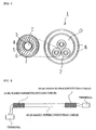
- a superconducting cable 1 of the present invention is configured such that cable cores 2 are housed in a thermal insulation tube 8.
- Each cable core 2 includes, from the inner side to the outer side, a former 3, a first conductor layer 4, and an insulating layer 5.
- a second conductor layer 6 and a protective layer 7 may also be sequentially disposed around the external periphery of the insulating layer 5. While a three-phase core high temperature superconducting cable is used in this embodiment, a single-core cable may be used.
- An aluminum, copper, or stainless pipe is used for the former 3, which is the innermost portion of the cable core 2.
- a strand of metal lines such as narrow copper lines, may be employed. If the pipe is used, the internal portion I of the former can be used as a cooling medium path. If narrow copper lines are used, each copper line is preferably coated with an insulating material for reducing the eddy current loss.
- An RE superconductor is used as the superconductor for the first and second conductor layers 4 and 6, respectively.
- a tape-shaped superconductor obtained by forming an RE superconductor layer on a metal substrate is suitable as the superconductor wire.
- the first conductor layer is formed by being helically wound around or being attached parallel to the former.
- the second conductor layer is formed by being helically wound around or being attached parallel to the insulating layer.
- the first conductor layer 4 is used as a cable conductor
- the second conductor layer 6 is used as a shielding layer.
- the protective layer 7 may also be disposed on the second conductor layer 6.
- the insulating layer 5 is configured such that a cooling medium is soaked in a wound insulating material.
- the insulating material includes insulating paper, such as kraft paper, semi-synthetic paper, such as Polypropylene Laminated Paper (PPLP), formed by laminating kraft paper at least to one side of a polypropylene film, and synthetic paper, such as a polyethylen film or a polypropylene film. Liquid helium or liquid nitrogen is used as the cooling medium.
- the thermal insulation tube 8 may be configured in any manner provided that a sufficient thermal insulation property is exhibited. Generally, however, a double structure formed of a corrugated inner tube and outer tube is employed. A thermal insulating material, such as super insulation, is disposed between the inner tube and the outer tube and the space therebetween is kept in a vacuum state so as to form an insulating layer. A space O formed between the thermal insulation tube 8 and each core 2 serves as a cooling medium path.
- a protection layer may also be formed for protecting the thermal insulation tube 8.
- PVC polyvinyl chloride
- Ten YBa 2 Cu 3 O x (YBCO) superconducting tape wires having a width of 5 mm and a thickness of about 0.1 mm were spirally wound at a 300 mm pitch around a stainless pipe having an inner diameter of 20 mm ⁇ , an outer diameter of 24 mm ⁇ , and a length of 2 m, thereby forming a single-layered Y based superconducting cable conductor.
- the superconducting tape wires were configured such that a 2 ⁇ m-YBCO superconducting layer was formed on a stainless substrate having a width of 5 mm and a thickness of 0.1 mm via a 1 ⁇ m-YSZ intermediate layer and the surface thereof was sheathed with 5 ⁇ m silver, and the critical current thereof in liquid nitrogen was about 40 A.
- the layers within the range of 30 cm from the respective terminals of the superconducting cable were integrated by soldering with a copper lead wire attached thereto for causing a current to flow.
- a DC current-carrying test was conducted by soaking this conductor in liquid nitrogen.
- the critical current defined by the generation of an electric resistance with a criterion of 1 ⁇ V/cm was 400 A.
- Bi based superconducting silver sheathed tape wires having a width of 4 mm and a thickness of about 0.3 mm were spirally wound at a 300 mm pitch around a stainless pipe having a configuration similar to that used in the second embodiment, thereby forming a single-layered Bi based superconducting cable conductor.
- the Bi based superconducting silver sheathed tape wires were configured such that 61 Bi 2 Sr 2 Ca 2 Cu 3 O x superconducting layers having a width of about 30 ⁇ m were embedded in a silver matrix having a width of 4 mm and a thickness of about 0.3 mm, and the critical current thereof in liquid nitrogen was about 50 A.
- the layers within the range of 30 cm from the respective terminals of the superconducting cable conductor were integrated by soldering with a copper lead wire attached thereto for causing a current to flow.
- a DC current-carrying test was conducted by soaking this conductor in liquid nitrogen.
- the critical current defined by the generation of an electric resistance with a criterion with 1 ⁇ V/cm was 500 A.
- the current-voltage (I-V) characteristic was measured by separately connecting the two conductors of this embodiment and the comparative example to an AC power source, and by supplying the AC up to ten times higher than the critical current to the conductors.
- the results are as follows.
- the AC reached 1000 A the current was suppressed by the generation of an electric current by the quenching of the conductor, and a current of 1500 A or higher did not flow in the conductor. That is, the implementation of a current limiting function was observed.
- HoBa 2 Cu 3 O x (HoBCO) superconducting tape wires having a width of 5 mm and a thickness of about 0.1 mm were spirally wound at a 400 mm pitch around a copper pipe having an inner diameter of 26 mm ⁇ , an outer diameter of 30 mm ⁇ , and a length of 1 m, and thereby two layers of HoBCO superconducting cable conductors were formed.
- HoBCO HoBa 2 Cu 3 O x
- the HoBCO superconducting tape wires were configured such that a 3 ⁇ m-HoBCO superconducting layer was formed on a stainless substrate having a width of 5 mm and a thickness of 0.1 mm via a 1 ⁇ m-YSZ intermediate layer and the surface of the layer was sheathed with 5 ⁇ m silver, and their critical current in liquid nitrogen was about 50 A.
- An insulating layer having a thickness of 5 mm was formed between the first and second layers by wrapping, in half-overlap, 10 layers of kraft paper having a thickness of 0.2 mm. The first and second layers were wound in opposite directions.
- the layers within the range of 30 cm from the respective terminals of the superconducting cable conductor were integrated by soldering with a copper lead wire attached thereto for causing a current to flow.
- a DC current-carrying test was conducted by soaking this conductor in liquid nitrogen, and the critical current defined by the generation of an electric resistance with a criterion of 1 ⁇ V/cm was 1000 A for both the first and second layers.
- Ten Bi based superconducting silver sheathed tape wires having a width of 4 mm and a thickness of about 0.3 mm (in which 61 Bi2223 superconducting layers having a width of about 30 ⁇ m were embedded in a silver matrix having a width of 4 mm and a thickness of 0.3 mm, and the critical current in liquid nitrogen was about 50 A) were spirally wound at a 300 mm pitch around a stainless corrugated pipe having an inner diameter of 26 mm ⁇ , an outer diameter of 30 mm ⁇ , and a length of 1 m, and thereby a first layer of Bi based superconducting cable conductor was formed.
- An insulating layer having a thickness of 5 mm was formed by wrapping, in half-overlap, ten layers of kraft paper having a thickness of 0.2 mm between the first and second layers, the second conductor layer being formed in the same configuration as the first layer except that their winding pitch was in opposite directions each other.
- the layers within the range of 30 cm from the terminals of the superconducting cable conductor were integrated by soldering with a copper lead wire attached thereto for causing a current to flow.
- a DC current-carrying test was conducted by soaking this conductor in liquid nitrogen, and the critical current defined by the generation of an electrical resistance with a criterion of 1 ⁇ V/cm was 1000 A for both the first and second layers.
- the current-voltage (I-V) characteristic was measured by separately connecting the two conductors to an AC power source, and by supplying the AC up to five times higher than the critical current to the conductors.
- the results are as follows.
- the AC reached 1000 A the current was suppressed by the generation of an electric current by the quenching of the conductor, and the current of 1500 A or higher did not flow in the conductor. That is, the implementation of a current limiting function was observed.
- two 1 m-length RE based superconducting cables (current limiters) 10 described in the third embodiment and one 10 m-length Bi based superconducting cable (base) 20 described in the third embodiment were prepared, and the RE based superconducting cables were disposed at the two ends of the Bi based superconducting cable.
- the first layer was configured by the connection of the cables such that a conductor current flows, and the second layer was configured by the connection of the cables such that a shield current flows.
- an RE based superconducting wire is used, and thus, a fail-safe current limiting function is implemented by generating an electrical resistance when the current of a conductor layer exceeds the critical current, thereby preventing the cable from being damaged.
- a cable line having a base and a current limiter using the cable of the present invention is enabled to have automatic damping of current when a current higher than the rated current of the base flows.
Landscapes
- Superconductors And Manufacturing Methods Therefor (AREA)
- Emergency Protection Circuit Devices (AREA)
Abstract
Description
Claims (11)
- A superconducting cable whose core comprises a first conductor layer formed of superconducting wires, and an insulating layer formed on the outer periphery of said first conductor layer, wherein said first conductor layer is an assembly of a plurality of superconducting wires made by forming an RE based superconductor layer on a metal substrate.
- A superconducting cable according to claim 1, further comprising a second conductor layer provided on the outer periphery of said insulating layer, wherein said second conductor layer is an assembly of a plurality of superconducting wires made by forming an RE based superconductor layer on a metal substrate.
- A superconducting cable according to claim 2, wherein said first conductor layer is a cable conductor layer, and said second conductor layer is a cable shielding layer.
- A superconducting cable according to claim 1, wherein the superconducting wire has an intermediate layer between the metal substrate and the RE based superconducting layer.
- A superconducting cable line using a superconducting cable, wherein said superconducting cable comprises a base and a current limiter for damping a current which exceeds a rated current of said base, the current limiter being formed of the superconducting cable set forth in claim 1.
- A superconducting cable line using a superconducting cable, wherein said superconducting cable comprises a base and a current limiter for damping a current which exceeds a rated current of said base, the current limiter being formed of the superconducting cable set forth in claim 2.
- A superconducting cable line using a superconducting cable, wherein said superconducting cable comprises a base and a current limiter for damping a current which exceeds a rated current of said base, the current limiter being formed of the superconducting cable set forth in claim 3.
- A superconducting cable line using a superconducting cable, wherein said superconducting cable comprises a base and a current limiter for damping a current which exceeds a rated current of said base, the current limiter being formed of the superconducting cable set forth in claim 4.
- A superconducting cable line according to claim 5, wherein the current limiter is provided at a terminal or an intermediate connecting portion of said base.
- A superconducting cable line according to claim 5, wherein the superconducting wire of said base is formed of a superconductor different from an RE based superconductor.
- A superconducting cable comprising a cable core housed in a thermal insulation tube, said cable core comprising: a first conductor layer disposed on the outer periphery of a former, said first conductor layer being an assembly formed of a plurality of superconducting wires obtained by forming an RE based superconducting layer on a metal substrate; an insulating layer disposed on the outer periphery of said first conductor layer; a second conductor layer disposed on the outer periphery of said insulating layer, said second conductor layer being an assembly formed of a plurality of superconducting wires obtained by forming an RE superconducting layer on a metal substrate; and a protective layer disposed on the outer periphery of said second conductor layer.
Applications Claiming Priority (3)
| Application Number | Priority Date | Filing Date | Title |
|---|---|---|---|
| JP2001338470A JP2003141946A (en) | 2001-11-02 | 2001-11-02 | Superconducting cable |
| JP2001338470 | 2001-11-02 | ||
| PCT/JP2002/010562 WO2003038840A1 (en) | 2001-11-02 | 2002-10-10 | Superconducting cable and superconducting cable line |
Publications (3)
| Publication Number | Publication Date |
|---|---|
| EP1441366A1 true EP1441366A1 (en) | 2004-07-28 |
| EP1441366A4 EP1441366A4 (en) | 2006-12-20 |
| EP1441366B1 EP1441366B1 (en) | 2013-04-03 |
Family
ID=19152959
Family Applications (1)
| Application Number | Title | Priority Date | Filing Date |
|---|---|---|---|
| EP02802359A Expired - Lifetime EP1441366B1 (en) | 2001-11-02 | 2002-10-10 | Superconducting cable and superconducting cable line |
Country Status (8)
| Country | Link |
|---|---|
| US (1) | US7149560B2 (en) |
| EP (1) | EP1441366B1 (en) |
| JP (1) | JP2003141946A (en) |
| KR (1) | KR100938357B1 (en) |
| CN (1) | CN1264171C (en) |
| CA (1) | CA2439947C (en) |
| TW (1) | TW589644B (en) |
| WO (1) | WO2003038840A1 (en) |
Families Citing this family (27)
| Publication number | Priority date | Publication date | Assignee | Title |
|---|---|---|---|---|
| JP4399763B2 (en) * | 2003-02-28 | 2010-01-20 | 住友電気工業株式会社 | DC superconducting cable line |
| JP4207223B2 (en) | 2003-06-19 | 2009-01-14 | 住友電気工業株式会社 | Superconducting cable and superconducting cable line using this superconducting cable |
| JP4298450B2 (en) * | 2003-09-24 | 2009-07-22 | 住友電気工業株式会社 | Superconducting cable terminal structure |
| US7608785B2 (en) | 2004-04-27 | 2009-10-27 | Superpower, Inc. | System for transmitting current including magnetically decoupled superconducting conductors |
| US7933260B2 (en) * | 2004-06-29 | 2011-04-26 | Damaka, Inc. | System and method for routing and communicating in a heterogeneous network environment |
| JP4689984B2 (en) * | 2004-07-20 | 2011-06-01 | 株式会社ワイ・ワイ・エル | DC superconducting power transmission cable and power transmission system |
| JP4609121B2 (en) | 2004-07-29 | 2011-01-12 | 住友電気工業株式会社 | Superconducting cable line |
| JP4835821B2 (en) * | 2004-11-02 | 2011-12-14 | 住友電気工業株式会社 | Superconducting cable |
| KR100586570B1 (en) * | 2004-11-25 | 2006-06-07 | 엘에스전선 주식회사 | Superconducting Wire with Crack Resistant Structure |
| JP4716246B2 (en) * | 2004-12-01 | 2011-07-06 | 住友電気工業株式会社 | Superconducting cable |
| JP4730583B2 (en) | 2004-12-01 | 2011-07-20 | 住友電気工業株式会社 | Superconducting cable line |
| JP4609638B2 (en) * | 2004-12-06 | 2011-01-12 | 住友電気工業株式会社 | DC superconducting cable design system |
| US7943852B2 (en) * | 2005-03-14 | 2011-05-17 | Sumitomo Electric Industries, Ltd. | Superconducting cable |
| RU2388090C2 (en) * | 2005-03-14 | 2010-04-27 | Сумитомо Электрик Индастриз, Лтд. | Superconducting cable and system for transfer of direct current that comprises this superconducting cable |
| JP5115778B2 (en) * | 2006-01-16 | 2013-01-09 | 住友電気工業株式会社 | Superconducting cable |
| KR100706494B1 (en) * | 2006-01-20 | 2007-04-10 | 엘에스전선 주식회사 | Superconducting cable |
| US20080194411A1 (en) * | 2007-02-09 | 2008-08-14 | Folts Douglas C | HTS Wire |
| US20080190646A1 (en) * | 2007-02-09 | 2008-08-14 | Folts Douglas C | Parallel connected hts fcl device |
| US20080191561A1 (en) * | 2007-02-09 | 2008-08-14 | Folts Douglas C | Parallel connected hts utility device and method of using same |
| JP4967750B2 (en) * | 2007-03-28 | 2012-07-04 | 住友電気工業株式会社 | Superconducting cable connection structure and superconducting cable connection method |
| MX2012014420A (en) | 2010-06-22 | 2013-02-26 | Abb Research Ltd | Electrical conductor with surrounding electrical insulation. |
| US8774883B2 (en) * | 2010-12-02 | 2014-07-08 | Lighthouse Energy Solutions LLC | Superconducting direct current transmission system |
| US9608431B2 (en) * | 2010-12-02 | 2017-03-28 | Lighthouse Energy Solutions LLC | System and method to interrupt a DC current in a high voltage circuit by use of an AC circuit breaker |
| US8938278B2 (en) * | 2011-02-18 | 2015-01-20 | The Regents Of The University Of Colorado | Superconducting cables and methods of making the same |
| CN107800123B (en) * | 2017-11-13 | 2019-11-15 | 北京交通大学 | Main insulation structure device and method of a vertical high temperature superconducting resistance current limiter |
| CN108039248B (en) * | 2017-12-08 | 2020-08-14 | 北京原力辰超导技术有限公司 | High-temperature superconducting cable with composite electromagnetic shielding layer |
| CN110265802B (en) * | 2019-06-19 | 2020-07-14 | 东部超导科技(苏州)有限公司 | Superconducting cable end connecting structure based on YBCO superconducting material |
Family Cites Families (34)
| Publication number | Priority date | Publication date | Assignee | Title |
|---|---|---|---|---|
| GB1340983A (en) * | 1971-03-10 | 1973-12-19 | Siemens Ag | Superconductor cables |
| US4184042A (en) * | 1977-05-03 | 1980-01-15 | Gosudarstvenny Nauchno-Issledovatelsky Energetichesky Institut Imeni G.M. Krzhizhanovskogo | Multisection superconducting cable for carrying alternating current |
| JPS6489130A (en) * | 1987-09-29 | 1989-04-03 | Nippon Kouatsu Electric Co | Current limiting fuse using high temperature oxide superconductor |
| JPH01161614A (en) * | 1987-12-17 | 1989-06-26 | Toshiba Corp | Superconducting current limiting element |
| SE461306B (en) * | 1988-06-10 | 1990-01-29 | Asea Brown Boveri | STROEMBEGRAENSARE |
| DE3822684A1 (en) * | 1988-07-05 | 1990-01-11 | Asea Brown Boveri | ELECTRIC LADDER IN WIRE OR CABLE FORM, CONSTRUCTED FROM A SHEATHED WIRE OR MULTIPLE FILM LADDER BASED ON A CERAMIC HIGH TEMPERATURE SUPER LADDER |
| CH677549A5 (en) * | 1988-08-02 | 1991-05-31 | Asea Brown Boveri | |
| US4932523A (en) * | 1989-05-26 | 1990-06-12 | Wataru Yamazoe | Protective box-shaped tube for inserting a golf club into a golf bag |
| JPH0653037A (en) * | 1992-07-31 | 1994-02-25 | Furukawa Electric Co Ltd:The | Oxide superconductor current lead |
| JPH06243737A (en) * | 1993-02-18 | 1994-09-02 | Asahi Glass Co Ltd | Oxide superconducting coil |
| JPH07169343A (en) * | 1993-10-21 | 1995-07-04 | Sumitomo Electric Ind Ltd | Superconducting cable conductor |
| FR2723467B1 (en) * | 1994-08-04 | 1997-01-03 | Alsthom Cge Alcatel | SUPERCONDUCTING ELECTRICAL LINK |
| US6077344A (en) * | 1997-09-02 | 2000-06-20 | Lockheed Martin Energy Research Corporation | Sol-gel deposition of buffer layers on biaxially textured metal substances |
| US6716795B2 (en) * | 1999-09-27 | 2004-04-06 | Ut-Battelle, Llc | Buffer architecture for biaxially textured structures and method of fabricating same |
| JP4044635B2 (en) * | 1996-10-16 | 2008-02-06 | 新日本製鐵株式会社 | Superconducting fault current limiter |
| GB9705717D0 (en) * | 1997-03-19 | 1997-05-07 | Rolls Royce Power Eng | Resistive superconducting current limiter |
| US6440211B1 (en) * | 1997-09-02 | 2002-08-27 | Ut-Battelle, Llc | Method of depositing buffer layers on biaxially textured metal substrates |
| US6596945B1 (en) * | 1998-09-11 | 2003-07-22 | Southwire Company | Superconducting cable |
| US6296701B1 (en) * | 1998-09-30 | 2001-10-02 | Ut-Battelle, Llc | Method of depositing an electrically conductive oxide film on a textured metallic substrate and articles formed therefrom |
| WO2000049665A1 (en) * | 1999-02-17 | 2000-08-24 | Solvay Barium Strontium Gmbh | Superconductive bodies made of zinc-doped copper oxide material |
| JP3521182B2 (en) * | 1999-02-26 | 2004-04-19 | 株式会社東芝 | Oxide superconducting wire and superconducting device |
| JP2003500985A (en) * | 1999-05-17 | 2003-01-07 | エヌケイティ リサーチ アクティーゼルスカブ | Overcurrent protection method for superconducting cables. |
| GB2350485A (en) * | 1999-05-28 | 2000-11-29 | Asea Brown Boveri | A fault current limiter |
| JP2001006837A (en) | 1999-06-16 | 2001-01-12 | Sumitomo Electric Ind Ltd | Branch structure of dc superconducting cable |
| US6864430B2 (en) * | 1999-09-09 | 2005-03-08 | Southwire Company | Superconducting cable having a flexible former |
| AU1130301A (en) * | 1999-10-29 | 2001-05-14 | Nkt Research Center A/S | Method of producing a superconducting cable |
| EP1234312A1 (en) * | 1999-10-29 | 2002-08-28 | NKT Cables A/S | Method of producing a superconducting cable |
| JP4487361B2 (en) * | 2000-01-20 | 2010-06-23 | 住友電気工業株式会社 | Superconducting cable |
| JP2002100249A (en) * | 2000-07-21 | 2002-04-05 | Furukawa Electric Co Ltd:The | Superconducting cable for AC |
| ATE293280T1 (en) * | 2000-08-14 | 2005-04-15 | Pirelli & C Spa | SUPERCONDUCTING CABLE |
| AU2001293678A1 (en) * | 2000-10-02 | 2002-04-15 | Nkt Cables Ultera A/S | A terminal connection for a superconductive cable |
| JP4713012B2 (en) * | 2000-10-31 | 2011-06-29 | 財団法人国際超電導産業技術研究センター | Tape-shaped oxide superconductor |
| US6745059B2 (en) * | 2001-11-28 | 2004-06-01 | American Superconductor Corporation | Superconductor cables and magnetic devices |
| US6849580B2 (en) * | 2003-06-09 | 2005-02-01 | University Of Florida | Method of producing biaxially textured buffer layers and related articles, devices and systems |
-
2001
- 2001-11-02 JP JP2001338470A patent/JP2003141946A/en active Pending
-
2002
- 2002-10-10 EP EP02802359A patent/EP1441366B1/en not_active Expired - Lifetime
- 2002-10-10 CN CNB028044096A patent/CN1264171C/en not_active Expired - Fee Related
- 2002-10-10 CA CA2439947A patent/CA2439947C/en not_active Expired - Fee Related
- 2002-10-10 KR KR1020037009934A patent/KR100938357B1/en not_active Expired - Fee Related
- 2002-10-10 WO PCT/JP2002/010562 patent/WO2003038840A1/en not_active Ceased
- 2002-10-10 US US10/470,418 patent/US7149560B2/en not_active Expired - Lifetime
- 2002-10-25 TW TW091124902A patent/TW589644B/en not_active IP Right Cessation
Also Published As
| Publication number | Publication date |
|---|---|
| CN1264171C (en) | 2006-07-12 |
| EP1441366B1 (en) | 2013-04-03 |
| CN1489769A (en) | 2004-04-14 |
| TW589644B (en) | 2004-06-01 |
| JP2003141946A (en) | 2003-05-16 |
| CA2439947A1 (en) | 2003-05-08 |
| KR100938357B1 (en) | 2010-01-22 |
| CA2439947C (en) | 2012-07-10 |
| EP1441366A4 (en) | 2006-12-20 |
| US7149560B2 (en) | 2006-12-12 |
| WO2003038840A1 (en) | 2003-05-08 |
| US20040058822A1 (en) | 2004-03-25 |
| KR20040045394A (en) | 2004-06-01 |
Similar Documents
| Publication | Publication Date | Title |
|---|---|---|
| EP1441366B1 (en) | Superconducting cable and superconducting cable line | |
| US7071148B1 (en) | Joined superconductive articles | |
| EP0935261B1 (en) | Resistive fault current limiter | |
| KR101156972B1 (en) | A system for transmitting current including magnetically decoupled superconducting conductors | |
| EP1034581B1 (en) | A power induction device | |
| US7743485B1 (en) | Method of manufacturing a superconducting cable | |
| AU1965599A (en) | High voltage induction device | |
| US7633014B2 (en) | Superconductor cable | |
| AU1965699A (en) | Magnetic energy storage | |
| EP1323172A2 (en) | Superconducting cable | |
| US20030178653A1 (en) | Low alternating current (ac) loss superconducting coils | |
| US7417192B2 (en) | Superconductor components | |
| GB2350485A (en) | A fault current limiter |
Legal Events
| Date | Code | Title | Description |
|---|---|---|---|
| PUAI | Public reference made under article 153(3) epc to a published international application that has entered the european phase |
Free format text: ORIGINAL CODE: 0009012 |
|
| 17P | Request for examination filed |
Effective date: 20030731 |
|
| AK | Designated contracting states |
Kind code of ref document: A1 Designated state(s): AT BE BG CH CY CZ DE DK EE ES FI FR GB GR IE IT LI LU MC NL PT SE SK TR |
|
| AX | Request for extension of the european patent |
Extension state: AL LT LV MK RO SI |
|
| A4 | Supplementary search report drawn up and despatched |
Effective date: 20061120 |
|
| 17Q | First examination report despatched |
Effective date: 20101216 |
|
| GRAP | Despatch of communication of intention to grant a patent |
Free format text: ORIGINAL CODE: EPIDOSNIGR1 |
|
| RBV | Designated contracting states (corrected) |
Designated state(s): CH DE DK FR GB IT LI |
|
| GRAS | Grant fee paid |
Free format text: ORIGINAL CODE: EPIDOSNIGR3 |
|
| GRAA | (expected) grant |
Free format text: ORIGINAL CODE: 0009210 |
|
| AK | Designated contracting states |
Kind code of ref document: B1 Designated state(s): CH DE DK FR GB IT LI |
|
| REG | Reference to a national code |
Ref country code: GB Ref legal event code: FG4D |
|
| REG | Reference to a national code |
Ref country code: CH Ref legal event code: EP |
|
| REG | Reference to a national code |
Ref country code: DE Ref legal event code: R096 Ref document number: 60244761 Country of ref document: DE Effective date: 20130529 |
|
| PG25 | Lapsed in a contracting state [announced via postgrant information from national office to epo] |
Ref country code: DK Free format text: LAPSE BECAUSE OF FAILURE TO SUBMIT A TRANSLATION OF THE DESCRIPTION OR TO PAY THE FEE WITHIN THE PRESCRIBED TIME-LIMIT Effective date: 20130403 |
|
| PLBE | No opposition filed within time limit |
Free format text: ORIGINAL CODE: 0009261 |
|
| STAA | Information on the status of an ep patent application or granted ep patent |
Free format text: STATUS: NO OPPOSITION FILED WITHIN TIME LIMIT |
|
| PG25 | Lapsed in a contracting state [announced via postgrant information from national office to epo] |
Ref country code: IT Free format text: LAPSE BECAUSE OF FAILURE TO SUBMIT A TRANSLATION OF THE DESCRIPTION OR TO PAY THE FEE WITHIN THE PRESCRIBED TIME-LIMIT Effective date: 20130403 |
|
| 26N | No opposition filed |
Effective date: 20140106 |
|
| REG | Reference to a national code |
Ref country code: DE Ref legal event code: R097 Ref document number: 60244761 Country of ref document: DE Effective date: 20140106 |
|
| REG | Reference to a national code |
Ref country code: CH Ref legal event code: PL |
|
| GBPC | Gb: european patent ceased through non-payment of renewal fee |
Effective date: 20131010 |
|
| PG25 | Lapsed in a contracting state [announced via postgrant information from national office to epo] |
Ref country code: CH Free format text: LAPSE BECAUSE OF NON-PAYMENT OF DUE FEES Effective date: 20131031 Ref country code: GB Free format text: LAPSE BECAUSE OF NON-PAYMENT OF DUE FEES Effective date: 20131010 Ref country code: LI Free format text: LAPSE BECAUSE OF NON-PAYMENT OF DUE FEES Effective date: 20131031 |
|
| REG | Reference to a national code |
Ref country code: FR Ref legal event code: ST Effective date: 20140630 |
|
| PG25 | Lapsed in a contracting state [announced via postgrant information from national office to epo] |
Ref country code: FR Free format text: LAPSE BECAUSE OF NON-PAYMENT OF DUE FEES Effective date: 20131031 |
|
| PGFP | Annual fee paid to national office [announced via postgrant information from national office to epo] |
Ref country code: DE Payment date: 20171004 Year of fee payment: 16 |
|
| REG | Reference to a national code |
Ref country code: DE Ref legal event code: R119 Ref document number: 60244761 Country of ref document: DE |
|
| PG25 | Lapsed in a contracting state [announced via postgrant information from national office to epo] |
Ref country code: DE Free format text: LAPSE BECAUSE OF NON-PAYMENT OF DUE FEES Effective date: 20190501 |