EP1439556A1 - Solid-state electrolytic capacitor and its manufacturing method - Google Patents
Solid-state electrolytic capacitor and its manufacturing method Download PDFInfo
- Publication number
- EP1439556A1 EP1439556A1 EP02777912A EP02777912A EP1439556A1 EP 1439556 A1 EP1439556 A1 EP 1439556A1 EP 02777912 A EP02777912 A EP 02777912A EP 02777912 A EP02777912 A EP 02777912A EP 1439556 A1 EP1439556 A1 EP 1439556A1
- Authority
- EP
- European Patent Office
- Prior art keywords
- capacitor
- anode
- forming
- solid electrolyte
- lead
- Prior art date
- Legal status (The legal status is an assumption and is not a legal conclusion. Google has not performed a legal analysis and makes no representation as to the accuracy of the status listed.)
- Withdrawn
Links
Images



Classifications
-
- H—ELECTRICITY
- H01—ELECTRIC ELEMENTS
- H01G—CAPACITORS; CAPACITORS, RECTIFIERS, DETECTORS, SWITCHING DEVICES, LIGHT-SENSITIVE OR TEMPERATURE-SENSITIVE DEVICES OF THE ELECTROLYTIC TYPE
- H01G9/00—Electrolytic capacitors, rectifiers, detectors, switching devices, light-sensitive or temperature-sensitive devices; Processes of their manufacture
- H01G9/004—Details
- H01G9/008—Terminals
- H01G9/012—Terminals specially adapted for solid capacitors
-
- H—ELECTRICITY
- H01—ELECTRIC ELEMENTS
- H01G—CAPACITORS; CAPACITORS, RECTIFIERS, DETECTORS, SWITCHING DEVICES, LIGHT-SENSITIVE OR TEMPERATURE-SENSITIVE DEVICES OF THE ELECTROLYTIC TYPE
- H01G9/00—Electrolytic capacitors, rectifiers, detectors, switching devices, light-sensitive or temperature-sensitive devices; Processes of their manufacture
- H01G9/15—Solid electrolytic capacitors
-
- H—ELECTRICITY
- H01—ELECTRIC ELEMENTS
- H01G—CAPACITORS; CAPACITORS, RECTIFIERS, DETECTORS, SWITCHING DEVICES, LIGHT-SENSITIVE OR TEMPERATURE-SENSITIVE DEVICES OF THE ELECTROLYTIC TYPE
- H01G9/00—Electrolytic capacitors, rectifiers, detectors, switching devices, light-sensitive or temperature-sensitive devices; Processes of their manufacture
- H01G9/26—Structural combinations of electrolytic capacitors, rectifiers, detectors, switching devices, light-sensitive or temperature-sensitive devices with each other
Definitions
- the present invention relates to a solid electrolytic capacitor and a method of manufacturing the capacitor.
- a solid electrolytic capacitor placed in a secondary side of a power circuit, or close to a central processing unit (CPU) of a personal computer is required to have a large capacitance in a lower profile and a lower equivalent series resistance (ESR) as well as a lower equivalent series inductance (ESL).
- ESR equivalent series resistance
- ESL lower equivalent series inductance
- Fig. 16 is a sectional view of a conventional solid electrolytic capacitor.
- Dielectric layer 4 is formed of foil or sintered material 2 made of valve metal, such as tantalum, aluminum, and niobium, by anodization.
- Solid electrolyte layer 5 formed of oxide of transition metal, such as Mn, is formed on the surface of dielectric layer 4.
- Collector layer 6 is formed on the surface of solid electrolyte layer 5.
- Anode lead frame 8 is connected with lead portion 1 of an anode, while cathode lead frame 9 is connected with collector layer 6.
- the capacitor is covered with housing resin 7 to have anode lead frame 8 and cathode lead frame 9 exposed.
- the conventional solid electrolytic capacitor hardly includes a large volume of the anode for a large capacitance and hardly has a small ESR and a small ESL.
- a capacitor includes a valve metal foil including a valve metal porous body and a lead portion, a dielectric layer provided on the valve metal porous body, a solid electrolyte layer on the dielectric layer, a collector layer on the solid electrolyte layer, an anode lead connected to the lead portion, a housing for accommodating the valve metal porous body, the dielectric layer, the solid electrolyte layer, the collector layer, and the anode lead, and for having an end of the anode lead exposed from a surface of the housing, an anode external terminal provided over the housing and connected with the end of the anode lead, and a cathode external terminal provided over the housing and coupled with the collector layer.
- the capacitor has a large capacitance, a small ESR, and a small ESL.
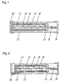
- Fig. 1 is a sectional view of a solid electrolytic capacitor in accordance with exemplary embodiment 1 of the present invention.
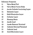
- the capacitor includes valve metal foil 11, valve metal porous body 12, and insulating layer 13 for electrically insulating between the anode and cathode to prevent the anode and cathode from short-circuited.
- porous body 12 is formed on both sides of foil 11, and insulating layer 13 is thus formed on both sides of foil 11. If porous body 12 is formed on one side of foil 11, insulating layer 13 is formed on the same side only.
- Dielectric layer 14 is formed on the surface of porous body 12 by anodization. Layer 14 may be formed of organic dielectric by an electro-deposition process.
- Solid electrolyte layer 15 is formed on the surface of dielectric layer 14 by chemical polymerization and/or electrolytic polymerization.
- Solid electrolyte layer 15 is made of conductive polymer, such as polypyrrole, polythiophene, and a derivative of each polymer.
- the conductive polymer forming solid electrolyte layer 15, since having a small resistibility, allows the solid electrolytic capacitor to have a small equivalent series resistance (ESR).
- Solid electrolyte layer 15 may be formed of manganese dioxide, which is generally used for the layer. In this case, layer 15 may be obtained by applying manganese nitrate to the surface of dielectric layer 14 and then performing heat decomposition to the surface.
- Polypyrrole and its derivative can be formed easily into a film having a uniform thickness, thus providung a solid electrolytic layer having a uniform thickness. As a result, a capacitor element can be easily accommodated in the solid electrolytic capacitor.
- Polythiophene and its derivative can be formed wasily into a solid electrolyte layer having a large heat resistance, thus providing a capacitor having a large heat resistance.
- Collector layer 16 made of carbon and conductive paste is formed on the surface of solid electrolyte layer 15.
- Housing resin 17 is formed of thermoset resin, such as epoxy, or thermoplastic resin having a large heat resistance.
- the conductive polymer formed by chemical polymerization forms the solid electrolyte layer in fine holes of the valve metal porous body, thus allowing the solid electrolytic capacitor to have a large capacitance efficiently.
- the conductive polymer is formed continuously on the surface of the dielectric layer by electrolytic polymerization, thus providing the solid electrolyte layer having fine-grained texture and a highly-protective coating.
- the solid electrolyte layer intimately contacts the collector layer, thus allowing the solid electrolytic capacitor to have a small ESR.
- Anode lead 18 made of aluminum or metal other than valve metal is electrically connected with foil 11 of valve metal.
- Anode external terminal 19 is electrically connected with anode lead 18.
- a lead portion made of the valve metal is easily oxidized at the outside of housing resin 17. To avoid the oxidization, the lead portion is connected to anode external terminal 19 through anode lead 18.
- Cathode external terminal 20 is electrically connected to collector layer 16. Both anode external terminal 19 and cathode external terminal 20 may be formed by plating or the like.
- Anode lead-out 18 made of the aforementioned material prevents anode lead 18a from having a strong oxide film having a large resistance formed on the surface of the lead 18a, thus allowing anode lead 18 to be easily connected with anode external terminal 19.
- Fig. 5 is a sectional view of the anode of the capacitor including valve metal foil 11 and valve metal porous body 12.
- Porous body 12 may be formed by screen-printing, dispensing, dye coating, powder-molding, or the like.
- valve metal porous body 12 is formed on both sides of valve metal foil 11, and anode-cathode insulating layer 13 is accordingly formed on both sides of foil 11. If porous body 12 is formed on one side of foil 11, insulating layer 13 is formed on the same side only.
- Insulating layer 13 may be formed after dielectric layer 14 is formed or after solid electrolyte layer 15 is formed. In the latter case, insulating layer 13 formed after dielectric layer 14 and solid electrolyte layer 15 are removed from the lead portion at which insulating layer 13 is supposed to be formed can further prevents the short-circuiting. If being formed after the dielectric layer, insulating layer 13 can be formed of material which may affect the formation of the dielectric layer. This expands a election range of the material, thereby increasing productivity of a solid electrolytic capacitor.
- dielectric layer 14 is formed on the surface of valve metal porous body 12 by anodization or electro-deposition process using organic dielectric.
- the anodization provides a polarized solid electrolytic capacitor, while the electro-deposition process provides a non-polarized solid electrolyte capacitor.
- solid electrolyte layer 15 made of the conductive polymer or manganese dioxide is formed on the surface of dielectric layer 14 by chemical polymerization, electrolytic polymerization, or heat decomposition of manganese nitrate.
- the chemical polymerization allows the thickness of the solid electrolyte layer to be proportional to an amount of applied electricity for the chemical polymerization, thus allowing the thickness of the layer to be easily controlled. As a result, the polymerization can provides the solid electrolyte layer with a small variations of the thickness from batch to batch.
- collector layer 16 is formed on the surface of solid electrolyte layer 15 with carbon and conductive paste similarly to a conventional process.
- anode lead 18 made of aluminum or metal other than valve metal is formed at a lead portion of the anode.
- Anode lead 18 may be formed before dielectric layer 14 is formed.
- housing resin 17 is formed to expose an end of anode lead 18 and a part of collector layer 16.
- Housing resin 17 is made of thermoplastic resin, such as epoxy, or a thermoplastic resin having a large heat resistance.
- anode external terminal 19 and cathode external terminal 20 are formed by electroplating or the like.
- Fig. 2 is a sectional view of a solid electrolytic capacitor in accordance with exemplary embodiment 2 of the present invention.
- the capacitor of the embodiment is differentiated from the capacitor of embodiment 1 shown in Fig. 1 in cathode lead 21.
- Cathode lead 21 electrically connects collector layer 16 with cathode external terminal 20.
- Cathode lead 21 is made of material of anode lead 18, i.e., aluminum or metal other than valve metal.
- Anode external terminal 19 and cathode external terminal 20 can be produced simultaneously at the same step, thereby simplifying processes of manufacturing the capacitor.
- an end of cathode lead-out 20 is exposed to the outside of housing resin 17 and is electrically connected with cathode external terminal 20.
- the capacitor of the embodiment is manufactured by processes shown in Fig. 5 to Fig. 9 of embodiment 1, and then by a process of forming cathode lead 21.
- Cathode lead 21 may be formed at any stage after collector layer 16 is formed and before housing resin 17 is formed.
- Fig. 3 is a sectional view of a solid electrolytic capacitor in accordance with exemplary embodiment 3 of the present invention.
- the capacitor of the embodiment is differentiated from the capacitor illustrated in Fig. 1 of embodiment 1 in including stacked capacitor elements.
- the stacked capacitor elements provide the solid electrolytic capacitor with a large capacitance. Additionally, a parallel connection of the capacitor elements decreases an equivalent serious resistance (ESR).
- ESR equivalent serious resistance
- the capacitor of the embodiment includes three capacitor elements stacked, but it is not limited to three. More capacitor elements provide the solid electrolytic capacitor with a larger capacitance and a smaller ESR.
- the capacitor of embodiment 2 includes the stacked capacitor elements formed through the process for forming collector layers 16, respectively, shown in Fig. 9 of embodiment 1.
- anode lead 18 is formed at respective lead portion, housing resin 17 is formed, and then, anode external terminal 19 and cathode external terminal 20 are formed.
- Anode lead 18 may be formed before the capacitor elements are stacked. This process allows anode lead 18 to be formed easily.
- Anode lead 18 may be formed before the dielectric layer is formed. Previously forming the anode lead at each lead portion not only simplify succeeding processes, but also reduces damage to the capacitor elements due to mechanical stress caused in forming the anode lead. This process can therefore decrease degradation of characteristics of a capacitor.
- the capacitor of the embodiments includes the anode lead having one end just exposed to the outside of the housing resin, while the conventional capacitor includes a lead frame that is bent over a part of the surface of the housing.
- the capacitor of the embodiments can includes more capacitor elements stacked than the conventional capacitor.
- the valve metal porous body may be formed on one surface of the valve metal foil.
- the anode-cathode insulating layer is formed on the side of the lead portion on which the porous body is formed. That is, the other side, on which the porous body is not formed, has no insulating layer thereon.
- Fig. 4 is a sectional view of a solid electrolytic capacitor in accordance with exemplary embodiment 4 of the present invention.
- the capacitor of the embodiment is differentiated from the capacitor shown in Fig. 3 of embodiment 3 in that the capacitor elements are stacked via solid electrolyte layers 15. That is, collector layer 16 is formed on the outer surfaces of solid electrolyte layers 15 of a stacked body including the stacked capacitor elements stacked via layer 15.
- the capacitor elements including solid electrolyte layer 15 formed through the process shown in Fig. 8 of embodiment 1 are stacked.
- collector layer 16 is formed, anode lead 18 is formed at each lead portion, housing resin 17 is formed, and then, anode external terminal 19 and cathode external terminal 20 are formed.
- Anode lead 18 may be formed before the capacitor elements are stacked. This process allows anode lead 18 to be formed on each element easily.
- Fig. 13 is a sectional view of a solid electrolytic capacitor in accordance with exemplary embodiment 5 of the present invention.
- the capacitor of embodiment 5 includes second solid electrolyte layer 30 on a solid electrolyte layer covering the outer surface of a stacked body including the stacked elements, while the capacitor of embodiment 4 includes capacitor elements stacked via solid electrolyte layers. This structure provides the stacked body with a large mechanical strength.
- the capacitor elements are stacked after solid electrolyte layer 15 is formed through the process shown in Fig. 8 of embodiment 1, and then, second solid electrolyte layer 30 is formed on the surface of the stacked capacitors.
- collector layer 16 is formed on the surface of second solid electrolyte layer 30, anode lead 18 is formed at each lead portion, housing resin 17 id formed, and then, anode external terminal 19 and cathode external terminal 20 are formed.
- Anode lead-out 18 may be formed before the capacitor elements are stacked. This process allows anode lead 18 to be formed on each element easily.
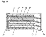
- Fig. 14 is a sectional view of a solid electrolytic capacitor in accordance with exemplary embodiment 6 of the present invention.
- the capacitor of embodiment 6 includes capacitor elements stacked via dielectric layer 14, while the capacitor of embodiment 3 shown in Fig. 3 includes a cathode portion of each capacitor element is stacked via collector layer 16. That is, according to embodiment 6, solid electrolyte layer 15 is formed at least on exposed surface of dielectric layer 14 of a stacked body including the capacitor elements stacked via layer 14.
- the capacitor elements are stacked after dielectric layer 14 is formed at the process shown in Fig. 7 of embodiment 1.
- Anode lead 18 may be formed before the capacitor elements including the layer 14 are stacked. This process allows anode lead 18 to be formed on each element easily.
- Example 1 of a capacitor corresponds to the capacitor of embodiment 1.
- Coating material was made of tantalum powder having an average particle diameter of 0.2 ⁇ m and a nominal capacitance of 100,000CV. Then, the material was applied in a thickness of 100 ⁇ m to both surfaces of a tantalum foil with a thickness of 25 ⁇ m with a metal mask having a hole of 5mm by 3mm formed therein. Then, the tantalum foil was dried to form the anode.
- the anode was degreased in nitric atmosphere at a temperature of 400°C, and then was baked in vacuum at a temperature of 1300°C.
- Anodecathode insulating layer 13 was formed of silicone at a lead portion of the anode. Then, dielectric layer 14 was formed by 12V-anodization in phosphoric acid solution.
- solid electrolyte layer 15 made of polythiophene derivative was formed on layer 14 by chemical polymerization. Further, a carbon layer and a silver paint layer were applied on the surface of layer 15 to form collector layer 16.
- housing 17 made of epoxy was formed so as to cover the capacitor element including anode lead 18.
- Anode external terminal 19 and cathode external terminal 20 were formed on each side surface of housing 17 by plating.
- aging was performed to provide the solid electrolytic capacitor (having a size of 7.3mm by 4.3mm by 0.5mm).
- Example 2 of a capacitor corresponds to the capacitor of embodiment 2.
- anode lead 18 was formed at a lead portion of an anode, and then, cathode lead 21 was formed on collector layer 16.
- Copper foil having a thickness of 100 ⁇ m was employed for cathode lead 21.
- Cathode lead 21 was bonded to collector layer 16 by conductive adhesive.
- housing 17 made of epoxy was formed so as to cover a capacitor element.
- Anode external terminal 19 and cathode external terminal 20 were formed on each side surface of housing 17 by plating. Then, aging was performed to provide the solid electrolytic capacitor (having a size of 7.3mm by 4.3mm by 0.5mm).
- Example 3 of a capacitor corresponds to the capacitor of embodiment 3.
- housing 17 made of epoxy was formed so as to cover the stacked elements.
- Anode external terminal 19 and cathode external terminal 20 were formed on each side surface of housing 17 by plating. Then, aging was performed to provide the solid electrolytic capacitor (having a size of 7.3mm by 4.3mm by 2.0mm).
- Example 4 of a capacitor corresponds to the capacitor of embodiment 3.
- example 1 Eight capacitor elements having collector layers 16, respectively, were stacked. Anode lead 18 was formed at a lead portion of each of the stacked capacitor elements. Then, similarly to example 1, the solid electrolytic capacitor was provided (having a size of 7.3mm by 4.3mm by 4.0mm).
- Example 4 of a capacitor corresponds to the capacitor of embodiment 4.
- Example 6 of a capacitor corresponds to the capacitor of embodiment 45.
- Solid electrolyte layer 15 made of polythiophene derivative was formed at least on an exposed outer surface of solid electrolyte layer 15 disposed on the stacked elements by chemical polymerization.
- collector layer 16 was formed on the surface of the stacked elements, and anode lead 18 was formed at a lead portion of each the capacitor elements. Then, similarly to example 1, the solid electrolytic capacitor was provided (having a size of 7.3mm by 4.3mm by 4.5mm).
- example 7 of a capacitor corresponds to the capacitor of embodiment 6.
- Fig. 15 is a sectional view of comparative example 1 of a solid electrolytic capacitor.
- Coating material was made of tantalum powder having an average particle diameter of 0.2 ⁇ m and a nominal capacitance of 100,000CV. Next, the coating material was applied in a thickness of 100 ⁇ m to both surfaces of a tantalum foil having a thickness of 25 ⁇ m with a metal mask having a hole of 5mm by 3mm formed therein. Then, the tantalum foil was dried to form an anode.
- Example 1 Ten capacitors for each of examples, example 1 to example 7, and comparative example 1, are measured in capacitance at 120Hz, in the ESR at 100kHz, and the ESL at 5MHz. Table 1 shows an average of measurements of the ten capacitors for each example.
- Example 1 1 102 26 4.18
- Example 2 1 103 28 4.21
- Example 3 4 407 9.0 4.12
- Example 4 8 811 4.4 4.13
- Example 5 9 898 4.0 4.11
- Example 6 9 906 3.6 4.12
- Example 7 10 1017 3.0 4.08 Comparative Example 1 1 68 33 7.07
- the capacitors of examples 1 and 2 includes the same number of capacitor elements as that of comparative example 1. Nevertheless, the capacitors of examples 1 and 2 have larger capacitances, smaller ESRs, and smaller ESL than those of the capacitor of comparative example 1. This is because the capacitors of examples 1 and 2 exclude lead frames 8 and 9 included in the conventional capacitor.
- the solid electrolytic capacitor according to the present invention can includes the anode having a large volume due to eliminating lead frames 8 and 9.
- the capacitor of the present invention has the small ESR and the small ESL since not having an ESR provided by lead frames 8 and 9 or an ESL provided by an extending length of lead frames 8 and 9 connected with external electrodes 19 and 20 to be loaded on characteristics of the capacitor.
- the capacitance increases substantially in proportional to the number of the stacked capacitor elements, while the ESR decreases substantially in inversely-proportional to the number of the capacitor elements, thus providing the measurements theoretically.
- the capacitors of examples 5 to 7 have substantially the same sizes and are differentiated from one another in the time the capacitor elements are stacked.
- the capacitor of example 7 including the capacitor elements stacked after dielectric layer 14 is formed more than the capacitors of examples 5 and 6. This is because capacitor elements stacked at an earlier stage of its manufacturing process has a reduced thickness between the layers of the stacked elements. That is, the capacitor elements can be stacked more in a limited space in a solid electrolytic capacitor, thus providing the capacitor with an advantage in its capacitance and ESR.
- any capacitor of examples 1 to 7 are clearly different from the capacitor of comparative example 1 in characteristics. Any of capacitors of the examples selected due to manufacturing process has characteristics superior to the capacitor of comparative example 1.
- the tantalum porous body is formed on both sides of the tantalum foil.
- the porous body may can be formed on one side only, and in this case, anode lead 18 formed on the side having porous body 12 allows the capacitor elements to be effectively stacked.
- tantalum is used for the valve metal, but it is not limited to.
- Other valve metal such as aluminum, niobium, titanium, and zirconium, can provide the same effect.
- a solid electrolytic capacitor according to the present invention since not including a lead frame, can include an anode having a large volume, thus having a large capacitance.
Landscapes
- Engineering & Computer Science (AREA)
- Power Engineering (AREA)
- Microelectronics & Electronic Packaging (AREA)
- Fixed Capacitors And Capacitor Manufacturing Machines (AREA)
Abstract
Description
| Number of Stacked Capacitor Elements | Capacitance (µF) | ESR (mΩ) | ESL (nH) | |
| Example 1 | 1 | 102 | 26 | 4.18 |
| Example 2 | 1 | 103 | 28 | 4.21 |
| Example 3 | 4 | 407 | 9.0 | 4.12 |
| Example 4 | 8 | 811 | 4.4 | 4.13 |
| Example 5 | 9 | 898 | 4.0 | 4.11 |
| Example 6 | 9 | 906 | 3.6 | 4.12 |
| Example 7 | 10 | 1017 | 3.0 | 4.08 |
| Comparative Example 1 | 1 | 68 | 33 | 7.07 |
Claims (89)
- A capacitor comprising:a valve metal foil including a valve metal porous body and a lead portion;a dielectric layer provided on said valve metal porous body;a solid electrolyte layer on said dielectric layer;a collector layer on said solid electrolyte layer;an anode lead connected to said lead portion;a housing for accommodating said valve metal porous body, said dielectric layer, said solid electrolyte layer, said collector layer, and said anode lead, and for having an end of said anode lead exposed from a surface thereof;an anode external terminal provided over said housing and connected with said end of said anode lead; anda cathode external terminal provided over said housing and coupled with said collector layer.
- The capacitor of claim 1, further comprising an anode-cathode insulating layer provided at said lead portion for insulating between said lead portion and said solid electrolyte layer and for insulating between said lead portion and said collector layer.
- The capacitor of claim 1, wherein said anode lead can be plated.
- The capacitor of claim 1, wherein said anode lead is connected to a side of said lead portion on which said valve metal porous body is provided.
- The capacitor of claim 1, wherein said anode lead comprises one of aluminum and metal other than valve metal.
- The capacitor of claim 1, wherein said anode external terminal comprises a plated film.
- The capacitor of claim 1, wherein said cathode external terminal comprises a plated film.
- The capacitor of claim 1, further comprising a cathode lead for connecting said collector layer with said cathode external terminal.
- The capacitor of claim 8, wherein said cathode lead comprises one of aluminum and metal other than valve metal.
- The capacitor of claim 1, wherein said solid electrolyte layer comprises conductive polymer.
- A capacitor comprising:a stacked body including a plurality of capacitor elements stacked, said plurality of capacitor elements respectively including
valve metals foil including valve metal porous bodies and lead portions, respectively,
dielectric layers provided on said valve metal porous bodies, respectively,
solid electrolyte layers provided on said dielectric layers, respectively, and
collector layers provided on said solid electrolyte layers, respectively;anode leads connected to said lead portions, respectively;a housing for accommodating said stacked body and said anode leads, and for having respective ends of said anode leads exposed from a surface thereof;an anode external terminal provided over said housing and connected with said respective ends of said anode leads; anda cathode external terminal provided over said housing and coupled with said collector layers. - The capacitor of claim 11, further comprising an anode-cathode insulating layer provided at said lead portions for insulating between said lead portions and said solid electrolyte layers and for insulating between said lead portions and said collector layers, respectively.
- The capacitor of claim 11, wherein said anode leads can be plated.
- The capacitor of claim 11, wherein said anode leads are connected to sides of said lead portions on which said valve metal porous bodies are provided, respectively.
- The capacitor of claim 11, wherein said anode leads comprise one of aluminum and metal other than valve metal.
- The capacitor of claim 11, wherein said anode external terminal comprises a plated film.
- The capacitor of claim 11, wherein said cathode external terminal comprises a plated film.
- The capacitor of claim 11 further includes cathode leads for connecting said collector layers with said cathode external terminal, respectively.
- The capacitor of claim 18, wherein said cathode leads comprise one of aluminum and metal other than valve metals.
- The capacitor of claim 11, wherein said solid electrolyte layers comprise conductive polymer.
- A capacitor comprising:a stacked body including a plurality of capacitor elements stacked, said plurality of capacitor elements respectively including
valve metal foils having valve metal porous bodies and lead portions, respectively,
dielectric layers provided on said valve metal porous bodies, respectively, and
first solid electrolyte layers provided on said dielectric layers, respectively;a collector layer provided over said stacked body;anode leads connected to said lead portions, respectively;a housing for accommodating said stacked body, said collector layer, and said anode leads, and for having respective ends of said anode leads exposed from a surface thereof;an anode external terminal provided over said housing and connected with said respective ends of said anode leads; anda cathode external terminal provided over said housing and coupled with said collector layer. - The capacitor of claim 21, further comprising a second solid electrolyte layer provided on said stacked body.
- The capacitor of claim 22, wherein said second solid electrolyte layer comprises conductive polymer.
- The capacitor of claim 21, further comprising an anode-cathode insulating layer provided at said lead portions for insulating between said lead portions and said solid electrolyte layers, and for insulating between said lead portions and said collector layer.
- The capacitor of claim 21, wherein said anode leads can be plated.
- The capacitor of claim 21, wherein said anode leads are connected to sides of said lead portions on which said valve metal porous bodies are provided, respectively.
- The capacitor of claim 21, wherein said anode leads comprise one of aluminum and metal other than valve metal.
- The capacitor of claim 21, wherein said anode external terminal comprises a plated film.
- The capacitor of claim 21, wherein said cathode external terminal comprises a plated film.
- The capacitor of claim 21, further comprising a cathode lead for connecting said collector layer with said cathode external terminal.
- The capacitor of claim 30, wherein said cathode lead comprises one of aluminum and metal other than valve metal.
- The capacitor of claim 21, wherein said first solid electrolyte layers comprise conductive polymer.
- A capacitor comprising:a stacked body including a plurality of capacitor elements stacked, said plurality of capacitor elements respectively including
valve metal foils including valve metal porous bodies and lead portions, respectively, and
dielectric layers provided on said valve metal porous bodies, respectively;a solid electrolyte layer provided on said stacked body;a collector layer provided on said solid electrolyte layer;anode leads connected to said lead portions, respectively;a housing for accommodating said stacked body, said collector layer, and said anode leads, and for having respective ends of said anode leads exposed from a surface thereof;an anode external terminal provided over said housing and connected with said respective ends of said anode leads; anda cathode external terminal provided over said housing and coupled with said collector layer. - The capacitor of claim 33, further comprising an anode-cathode insulating layer provided at said lead portions for insulating between said lead portions and said solid electrolyte layer, and for insulating between said lead portions and said collector layer.
- The capacitor of claim 33, wherein said anode leads can be plated.
- The capacitor of claim 33, wherein said anode leads are connected to sides of said lead portions on which said valve metal porous bodies are provided.
- The capacitor of claim 33, wherein said anode leads comprise one of aluminum and metal other than valve metal.
- The capacitor of claim 33, wherein said anode external terminal comprises a plated film.
- The capacitor of claim 33, wherein said cathode external terminal comprises a plated film.
- The capacitor of claim 33, further comprising a cathode lead for connecting said collector layer with said cathode external terminal.
- The capacitor of claim 40, wherein said cathode lead comprises one of aluminum and metal other than valve metal.
- The capacitor of claim 33, wherein said solid electrolyte layer comprises conductive polymer.
- The capacitor any one of claims 10, 20, 23, 32, and 42, wherein said conductive polymer includes polypyrrole or its derivative.
- The capacitor any one of claims 10, 20, 23, 32, and 42, wherein said conductive polymer includes polythiophene or its derivative.
- The capacitor any one of claims 10, 20, 23, 32, and 42, wherein said conductive polymer includes compound of polypyrrole or its derivative with polythiophene or its derivative.
- The capacitor any one of claims 10, 20, 23, 32, and 42, wherein said conductive polymer is formed by chemical polymerization.
- The capacitor any one of claims 10, 20, 23, 32, and 42, wherein said conductive polymer is formed by electrolytic polymerization.
- The capacitor any one of claims 10, 20, 23, 32, and 42, wherein said conductive polymer is formed by chemical polymerizations and electrolytic polymerization.
- A method of manufacturing a solid electrolytic capacitor, comprising the steps of:providing a valve metal foil including a valve metal porous body and a lead portion;forming a dielectric layer on the valve metal porous body;forming a solid electrolyte layer on the dielectric layer;forming a collector layer formed on the solid electrolyte layer;connecting an anode lead to the lead portion;forming a housing for accommodating the valve metal porous body, the dielectric layer, the solid electrolyte layer, the collector layer, and the anode lead, and for having an end of the anode lead exposed from a surface of the housing; andforming external electrodes over the housing, the external electrodes being connected with the end of the anode lead and the collector layer, respectively.
- The method of claim 49, wherein said step of connecting the anode lead is executed before said step of forming the dielectric layer.
- The method of claim 49, further comprising the step of
forming an anode-cathode insulating layer on the lead portion. - The method of claim 51, wherein said step of forming the anode-cathode insulating layer is executed before said step of forming the dielectric layer.
- The method of claim 51, wherein said step of forming the anode-cathode insulating layer is executed after said step of forming the dielectric layer.
- The method of claim 49, further comprising the step of
removing a portion of the dielectric layer over on the lead portion. - The method of claim 54, further comprising the step of
after said step of removing the portion of the dielectric layer, forming an anode-cathode insulating layer at a portion of the lead portion corresponding the removed portion of the dielectric layer. - The method of claim 49, further comprising the step of
removing a portion of the solid electrolyte layer over the lead portion. - The method of claim 56, further comprising the step of
after the step of removing the portion of the solid electrolyte layer, forming an anode-cathode insulating layer at a portion of the lead portion corresponding to the removed portion of the solid electrolyte layer. - The method of claim 49, further comprising the step of
forming a cathode lead between the collector layer with one of the external electrodes. - A method of manufacturing a solid electrolytic capacitor, comprising the steps of:providing a plurality of valve metal foils including valve metal porous bodies and lead portions, respectively;forming a plurality of capacitor elements, comprising the sub-steps of
forming dielectric layers on the valve metal porous bodies, respectively,
forming solid electrolyte layers on the dielectric layers, respectively, and
forming collector layers on the solid electrolyte layers respectively;forming a stacked body including the plurality of the capacitor elements stacked;connecting anode leads to the lead portions, respectively;forming a housing for accommodating the stacked body, and for having respective ends of the anode leads exposed from a surface of the housing;forming an anode external terminal over the housing, the anode external electrode being connected to the respective ends of the anode leads; andforming a cathode external terminal over the housing, the cathode external electrode being coupled to the collector layers. - The method of claim 59, further comprising the step of
forming an anode-cathode insulating layer on respective sides of the lead portions on which the valve metal porous bodies are provided. - The method of claim 59, wherein the lead portions include anode-cathode insulating layers thereon, respectively.
- The method of claim 61, wherein the anode-cathode insulating layers are provided on respective sides of the lead portions on which the valve metal porous bodies are provided.
- The method of claim 59, wherein said step of connecting the anode leads to the lead portions is executed before said step of forming the stacked body.
- The method of claim 59, wherein said step of forming the solid electrolyte layers comprises the sub-step of
forming the solid electrolyte layers by chemical polymerization. - The method of claim 59, wherein said step of forming the solid electrolyte layers comprises the sub-step of
forming the solid electrolyte layers by electrolytic polymerization. - The method of claim 59, wherein said step of forming the solid electrolyte layers comprises the sub-step of
forming the solid electrolyte layers by chemical polymerization and electrolytic polymerization. - The method of claim 59, further comprising the step of
forming a cathode lead between each of the collector layers and the cathode external electrode. - A method of manufacturing a solid electrolytic capacitor, comprising the steps of:providing a plurality of valve metal foils including valve metal porous bodies and lead portions, respectively;forming a plurality of capacitor elements, including the sub-steps of
forming dielectric layers on the valve metal porous bodies, respectively, and
forming first solid electrolyte layers on the dielectric layers, respectively;forming a stacked body including the plurality of the capacitor elements stacked;forming a collector layer over the stacked body;connecting anode leads to the lead portions, respectively;forming a housing for accommodating the stacked body, and for having respective ends of the anode leads exposed from a surface of the housing;forming an anode external terminal over the housing, said anode external electrode being connected to the respective ends of the anode leads; andforming a cathode external terminal over the housing, the cathode external electrode being coupled to the collector layer. - The method of claim 68, further comprising the step of
forming an anode-cathode insulating layer on respective sides of the lead portions on which the valve metal porous bodies are provided. - The method of claim 68, wherein the lead portions include anode-cathode insulating layers thereon, respectively.
- The method of claim 70, wherein the anode-cathode insulating layers are provided on respective sides of the lead portions on which the valve metal porous bodies are provided.
- The method of claim 68, wherein said step of connecting the anode leads is executed before said step of forming the stacked body.
- The method of claim 68, wherein said step of forming the first solid electrolyte layers includes the sub-step of
forming the first solid electrolyte layers by chemical polymerization. - The method of claim 68, wherein said step of forming the first solid electrolyte layers includes the sub-step of
forming the first solid electrolyte layers by electrolytic polymerization. - The method of claim 68, wherein said step of forming the first solid electrolyte layers includes the sub-step of
forming the first solid electrolyte layers by chemical polymerization and electrolytic polymerization. - The method of claim 68, further comprising the step of
forming a cathode lead between the collector layer and the cathode external electrode. - The method of claim 68, further comprising the step of
forming a second solid electrolyte layer on the stacked body. - The method of claim 77, wherein said step of forming the second solid electrolyte layer includes the sub-step of
forming the second solid electrolyte layer by chemical polymerization. - The method of claim 77, wherein said step of forming the second solid electrolyte layer includes the sub-step of
forming the second solid electrolyte layer by electrolytic polymerization. - The method of claim 77, wherein said step of forming the second solid electrolyte layer includes the sub-step of
forming the second solid electrolyte layer by chemical polymerization and electrolytic polymerization. - A method of manufacturing a solid electrolytic capacitor, comprising the steps of:forming a plurality of capacitor elements, including the sub-steps of
providing a plurality of valve metal foils having valve metal porous bodies and lead portions, respectively, and
forming dielectric layers on the valve metal porous bodies, respectively;forming a stacked body including the plurality of the capacitor elements stacked;forming a solid electrolyte layer on the stacked body;forming a collector layer on the solid electrolyte layer;connecting anode leads to the lead portions, respectively;forming a housing for accommodating the stacked body, and for having respective ends of the anode leads exposed from a surface of the housing;forming an anode external terminal over the housing, the anode external electrode being connected to the respective ends of the anode leads; andforming a cathode external terminal over the housing, the cathode external electrode being coupled to the collector layer. - The method of claim 81, further comprising the step of
forming an anode-cathode insulating layer on respective sides of the lead portions on which the valve metal porous bodies are provided. - The method of claim 81, wherein the lead portions include anode-cathode insulating layers thereon, respectively.
- The method of claim 83, wherein the anode-cathode insulating layers are provided on respective sides of the lead portions on which the valve metal porous bodies are provided.
- The method of claim 81, wherein said step connecting the anode leads is executed before said step of forming the stacked body.
- The method of claim 81, wherein said step of forming the solid electrolyte layer includes the sub-step of forming the solid electrolyte layer by chemical polymerization.
- The method of claim 81, wherein said step of forming the solid electrolyte layer includes the sub-step of
forming the solid electrolyte layer by electrolytic polymerization. - The method of claim 81, wherein said step of forming the solid electrolyte layer includes the sub-step of
forming the solid electrolyte layer by chemical polymerization and electrolytic polymerization. - The method of claim 81, further comprising the step of forming a cathode lead between the collector layer and the cathode external electrode.
Applications Claiming Priority (3)
| Application Number | Priority Date | Filing Date | Title |
|---|---|---|---|
| JP2001328820A JP2003133183A (en) | 2001-10-26 | 2001-10-26 | Solid electrolytic capacitor and method of manufacturing the same |
| JP2001328820 | 2001-10-26 | ||
| PCT/JP2002/010927 WO2003036671A1 (en) | 2001-10-26 | 2002-10-22 | Solid-state electrolytic capacitor and its manufacturing method |
Publications (2)
| Publication Number | Publication Date |
|---|---|
| EP1439556A1 true EP1439556A1 (en) | 2004-07-21 |
| EP1439556A4 EP1439556A4 (en) | 2007-10-24 |
Family
ID=19144820
Family Applications (1)
| Application Number | Title | Priority Date | Filing Date |
|---|---|---|---|
| EP02777912A Withdrawn EP1439556A4 (en) | 2001-10-26 | 2002-10-22 | SEMICONDUCTOR ELECTROLYTIC CAPACITOR AND METHOD OF MANUFACTURING THE SAME |
Country Status (5)
| Country | Link |
|---|---|
| US (1) | US6771488B2 (en) |
| EP (1) | EP1439556A4 (en) |
| JP (1) | JP2003133183A (en) |
| CN (1) | CN100359614C (en) |
| WO (1) | WO2003036671A1 (en) |
Cited By (1)
| Publication number | Priority date | Publication date | Assignee | Title |
|---|---|---|---|---|
| GB2414859A (en) * | 2003-09-02 | 2005-12-07 | Nec Tokin Corp | A laminated transmission-line device. |
Families Citing this family (46)
| Publication number | Priority date | Publication date | Assignee | Title |
|---|---|---|---|---|
| US6687117B2 (en) * | 2002-01-31 | 2004-02-03 | Wilson Greatbatch Technologies, Inc. | Electrolytes for capacitors |
| KR100653440B1 (en) * | 2002-08-03 | 2006-12-01 | 주식회사 케이엠더블유 | Bias-tee device and its center conductor device |
| JP2005166832A (en) * | 2003-12-01 | 2005-06-23 | Rohm Co Ltd | Solid-state electrolytic capacitor |
| TWI270905B (en) * | 2004-07-14 | 2007-01-11 | Sanyo Electric Co | Solid electrolytic condenser and manufacturing method of the same |
| TWI283879B (en) * | 2005-02-17 | 2007-07-11 | Sanyo Electric Co | Solid electrolytic capacitor and manufacturing method thereof |
| JP4553771B2 (en) * | 2005-03-29 | 2010-09-29 | 三洋電機株式会社 | Solid electrolytic capacitor and manufacturing method thereof |
| JP4553770B2 (en) * | 2005-03-29 | 2010-09-29 | 三洋電機株式会社 | Solid electrolytic capacitor and manufacturing method thereof |
| WO2006123597A1 (en) | 2005-05-18 | 2006-11-23 | Matsushita Electric Industrial Co., Ltd. | Digital signal processor |
| JP4671339B2 (en) * | 2005-06-29 | 2011-04-13 | ニチコン株式会社 | Multilayer solid electrolytic capacitor |
| JP4739864B2 (en) * | 2005-08-30 | 2011-08-03 | 三洋電機株式会社 | Capacitor and manufacturing method thereof |
| US8414962B2 (en) | 2005-10-28 | 2013-04-09 | The Penn State Research Foundation | Microcontact printed thin film capacitors |
| US8403858B2 (en) * | 2006-10-12 | 2013-03-26 | Perceptive Navigation Llc | Image guided catheters and methods of use |
| JP4448865B2 (en) * | 2007-03-19 | 2010-04-14 | ニチコン株式会社 | Manufacturing method of solid electrolytic capacitor |
| US7460358B2 (en) * | 2007-03-21 | 2008-12-02 | Avx Corporation | Solid electrolytic capacitor containing a protective adhesive layer |
| US7515396B2 (en) * | 2007-03-21 | 2009-04-07 | Avx Corporation | Solid electrolytic capacitor containing a conductive polymer |
| US7483259B2 (en) * | 2007-03-21 | 2009-01-27 | Avx Corporation | Solid electrolytic capacitor containing a barrier layer |
| US7833292B2 (en) * | 2007-05-01 | 2010-11-16 | Kemet Electronics Corporation | Channel method for forming a capacitor |
| US8081419B2 (en) * | 2007-10-17 | 2011-12-20 | Greatbatch Ltd. | Interconnections for multiple capacitor anode leads |
| US8675349B2 (en) * | 2011-12-14 | 2014-03-18 | Kennet Electronics Corporation | Stack capacitor having high volumetric efficiency |
| US9576734B2 (en) | 2011-12-14 | 2017-02-21 | Kemet Electronics Corporation | Vertical stack approach in low profile aluminum solid electrolytic capacitors |
| US8680959B2 (en) * | 2012-05-09 | 2014-03-25 | Hamilton Sundstrand Corporation | Immersion cooled inductor apparatus |
| WO2014168686A1 (en) * | 2013-02-19 | 2014-10-16 | Kemet Electronics Corporation | Solid electrolytic capacitor and method of manufacturing a solid electrolytic capacitor |
| CN103366960A (en) * | 2013-07-23 | 2013-10-23 | 日科能高电子(苏州)有限公司 | Solid electrolytic capacitor |
| JP2015230976A (en) * | 2014-06-05 | 2015-12-21 | 株式会社村田製作所 | Method for manufacturing solid electrolytic capacitor, and solid electrolytic capacitor |
| CN104465104A (en) * | 2014-11-27 | 2015-03-25 | 中国振华(集团)新云电子元器件有限责任公司 | Anode tantalum core of ultrathin tantalum capacitor and manufacturing method thereof |
| US9439278B2 (en) * | 2014-12-12 | 2016-09-06 | Deere & Company | Film capacitor having a package for heat transfer |
| CN113990661A (en) * | 2015-12-18 | 2022-01-28 | 凯米特电子公司 | Capacitor using film for packaging material thickness control and manufacturing method |
| JP6729179B2 (en) | 2016-08-25 | 2020-07-22 | 株式会社村田製作所 | Solid electrolytic capacitor element, solid electrolytic capacitor, method of manufacturing solid electrolytic capacitor element, and method of manufacturing solid electrolytic capacitor |
| JP2018032768A (en) * | 2016-08-25 | 2018-03-01 | 株式会社村田製作所 | Solid electrolytic capacitor element, solid electrolytic capacitor, method for manufacturing solid electrolytic capacitor element, and method for manufacturing solid electrolytic capacitor |
| CN109791844B (en) * | 2016-10-17 | 2021-10-26 | 株式会社村田制作所 | Solid electrolytic capacitor |
| WO2018088574A1 (en) * | 2016-11-14 | 2018-05-17 | 株式会社村田製作所 | Solid electrolytic capacitor element, solid electrolytic capacitor and method for producing solid electrolytic capacitor element |
| CN117012552A (en) | 2017-09-23 | 2023-11-07 | 日本蓄电器工业株式会社 | solid electrolytic capacitor |
| JP7245997B2 (en) * | 2017-10-31 | 2023-03-27 | パナソニックIpマネジメント株式会社 | Electrolytic capacitor and manufacturing method thereof |
| WO2019156995A1 (en) * | 2018-02-12 | 2019-08-15 | Avx Corporation | Solid electrolytic capacitor for a tantalum embedded microchip |
| WO2020033820A1 (en) * | 2018-08-10 | 2020-02-13 | Avx Corporation | Solid electrolytic capacitor formed from conductive polymer particles |
| EP3834217A4 (en) | 2018-08-10 | 2022-05-11 | KYOCERA AVX Components Corporation | Solid electrolytic capacitor containing an intrinsically conductive polymer |
| CN118280737A (en) | 2018-08-10 | 2024-07-02 | 京瓷Avx元器件公司 | Solid electrolytic capacitor comprising polyaniline |
| US11955294B2 (en) | 2018-12-11 | 2024-04-09 | KYOCERA AVX Components Corporation | Solid electrolytic capacitor containing an intrinsically conductive polymer |
| JP7063301B2 (en) * | 2019-03-28 | 2022-05-09 | 株式会社村田製作所 | Manufacturing method of solid electrolytic capacitor |
| US11270847B1 (en) | 2019-05-17 | 2022-03-08 | KYOCERA AVX Components Corporation | Solid electrolytic capacitor with improved leakage current |
| US11170940B2 (en) * | 2019-05-17 | 2021-11-09 | Samsung Electro-Mechanics Co., Ltd. | Tantalum capacitor |
| WO2021055707A1 (en) | 2019-09-18 | 2021-03-25 | Avx Corporation | Solid electroltyic capacitor for use at high voltages |
| DE112020006028T5 (en) | 2019-12-10 | 2022-10-06 | KYOCERA AVX Components Corporation | Solid electrolytic capacitor containing a pre-coating and an intrinsically conductive polymer |
| WO2021119088A1 (en) | 2019-12-10 | 2021-06-17 | Avx Corporation | Tantalum capacitor with increased stability |
| JP2021192407A (en) * | 2020-06-05 | 2021-12-16 | パナソニックIpマネジメント株式会社 | Method of manufacturing metallic film, method of manufacturing solid electrolytic capacitor, and solid electrolytic capacitor |
| US11631548B2 (en) | 2020-06-08 | 2023-04-18 | KYOCERA AVX Components Corporation | Solid electrolytic capacitor containing a moisture barrier |
Family Cites Families (11)
| Publication number | Priority date | Publication date | Assignee | Title |
|---|---|---|---|---|
| JP3451574B2 (en) * | 1995-05-19 | 2003-09-29 | ローム株式会社 | Manufacturing method of solid electrolytic capacitor with safety fuse |
| JP3055466B2 (en) * | 1996-06-20 | 2000-06-26 | 日本電気株式会社 | Manufacturing method of chip type solid electrolytic capacitor |
| CA2278643C (en) * | 1997-11-28 | 2012-02-07 | Showa Denko K.K. | Solid electrolytic capacitor and method for producing the same |
| JP2000049048A (en) * | 1998-07-31 | 2000-02-18 | Elna Co Ltd | Chip-type solid electrolytic capacitor and manufacture thereof |
| DE60033076T2 (en) * | 1999-04-16 | 2007-08-30 | Matsushita Electric Industrial Co., Ltd., Kadoma | Anodic electrode for electrolytic capacitor and process for its preparation |
| JP2000323357A (en) * | 1999-05-07 | 2000-11-24 | Matsushita Electric Ind Co Ltd | Chip type solid electrolytic capacitor |
| JP2001085273A (en) | 1999-09-10 | 2001-03-30 | Matsushita Electric Ind Co Ltd | Chip type solid electrolytic capacitor |
| US6602741B1 (en) * | 1999-09-14 | 2003-08-05 | Matsushita Electric Industrial Co., Ltd. | Conductive composition precursor, conductive composition, solid electrolytic capacitor, and their manufacturing method |
| US6552896B1 (en) * | 1999-10-28 | 2003-04-22 | Matsushita Electric Industrial Co., Ltd. | Solid electrolytic capacitor and method for manufacturing the same |
| TW516054B (en) * | 2000-05-26 | 2003-01-01 | Matsushita Electric Industrial Co Ltd | Solid electrolytic capacitor |
| US6504705B2 (en) * | 2000-10-12 | 2003-01-07 | Matsushita Electric Industrial Co., Ltd. | Electrolytic capacitor, circuit board containing electrolytic capacitor, and method for producing the same |
-
2001
- 2001-10-26 JP JP2001328820A patent/JP2003133183A/en active Pending
-
2002
- 2002-10-22 US US10/451,748 patent/US6771488B2/en not_active Expired - Fee Related
- 2002-10-22 WO PCT/JP2002/010927 patent/WO2003036671A1/en not_active Ceased
- 2002-10-22 EP EP02777912A patent/EP1439556A4/en not_active Withdrawn
- 2002-10-22 CN CNB028030893A patent/CN100359614C/en not_active Expired - Fee Related
Cited By (3)
| Publication number | Priority date | Publication date | Assignee | Title |
|---|---|---|---|---|
| GB2414859A (en) * | 2003-09-02 | 2005-12-07 | Nec Tokin Corp | A laminated transmission-line device. |
| GB2414859B (en) * | 2003-09-02 | 2006-03-08 | Nec Tokin Corp | Laminated transmission-line device |
| GB2405747B (en) * | 2003-09-02 | 2006-03-08 | Nec Tokin Corp | Laminated solid electrolytic capacitor. |
Also Published As
| Publication number | Publication date |
|---|---|
| EP1439556A4 (en) | 2007-10-24 |
| US20040066608A1 (en) | 2004-04-08 |
| CN1476621A (en) | 2004-02-18 |
| JP2003133183A (en) | 2003-05-09 |
| US6771488B2 (en) | 2004-08-03 |
| CN100359614C (en) | 2008-01-02 |
| WO2003036671A1 (en) | 2003-05-01 |
Similar Documents
| Publication | Publication Date | Title |
|---|---|---|
| US6771488B2 (en) | Solid electrolytic capacitor and method of manufacturing the capacitor | |
| US6563693B2 (en) | Solid electrolytic capacitor | |
| US20090116173A1 (en) | Solid electrolytic capacitor | |
| US6791822B2 (en) | Solid electrolytic capacitor | |
| JP2001185460A (en) | Solid electrolytic capacitor, method of manufacturing the same, and circuit board | |
| US20120281338A1 (en) | Aluminum electrolytic capacitor and method of manfacturing the same | |
| US7218505B2 (en) | Chip solid electrolyte capacitor | |
| US11521802B2 (en) | Solid electrolyte capacitor and fabrication method thereof | |
| US8218292B2 (en) | Dry powder stencil printing of solid electrolytic capacitor components | |
| EP3767654A1 (en) | Solid electrolytic capacitor and method for manufacturing solid electrolytic capacitor | |
| EP1654745B1 (en) | Chip solid electrolyte capcitor and production method of the same | |
| US7355842B2 (en) | Chip solid electrolyte capacitor and production method of the same | |
| JP2001126958A (en) | Chip-type solid electrolytic capacitor | |
| KR20050113628A (en) | Chip solid electrolyte capacitor | |
| JP3546451B2 (en) | Method for manufacturing solid electrolytic capacitor | |
| JP3185405B2 (en) | Solid electrolytic capacitors | |
| JP3441095B2 (en) | Solid electrolytic capacitors | |
| JP3505763B2 (en) | Chip-shaped solid electrolytic capacitor | |
| JPH10335187A (en) | Solid electrolytic capacitor and method of manufacturing the same | |
| JP3208875B2 (en) | Chip-shaped solid electrolytic capacitor and its manufacturing method | |
| KR20060058719A (en) | Chip-shaped solid electrolytic capacitors and manufacturing method thereof | |
| JP2001044078A (en) | Solid electrolytic capacitor | |
| JPH0740539B2 (en) | Array type solid electrolytic capacitor | |
| JPH07183170A (en) | Chip-shaped solid electrolytic capacitor | |
| JPH05291089A (en) | Multiple capacitor element |
Legal Events
| Date | Code | Title | Description |
|---|---|---|---|
| PUAI | Public reference made under article 153(3) epc to a published international application that has entered the european phase |
Free format text: ORIGINAL CODE: 0009012 |
|
| 17P | Request for examination filed |
Effective date: 20031229 |
|
| AK | Designated contracting states |
Kind code of ref document: A1 Designated state(s): AT BE BG CH CY CZ DE DK EE ES FI FR GB GR IE IT LI LU MC NL PT SE SK TR |
|
| A4 | Supplementary search report drawn up and despatched |
Effective date: 20070921 |
|
| RIC1 | Information provided on ipc code assigned before grant |
Ipc: H01G 9/08 20060101ALN20070917BHEP Ipc: H01G 9/15 20060101ALI20070917BHEP Ipc: H01G 9/052 20060101ALN20070917BHEP Ipc: H01G 9/012 20060101AFI20070917BHEP |
|
| RAP1 | Party data changed (applicant data changed or rights of an application transferred) |
Owner name: PANASONIC CORPORATION |
|
| 17Q | First examination report despatched |
Effective date: 20090116 |
|
| STAA | Information on the status of an ep patent application or granted ep patent |
Free format text: STATUS: THE APPLICATION IS DEEMED TO BE WITHDRAWN |
|
| 18D | Application deemed to be withdrawn |
Effective date: 20090527 |