EP1438744B1 - Method of forming a raised contact for a substrate - Google Patents
Method of forming a raised contact for a substrate Download PDFInfo
- Publication number
- EP1438744B1 EP1438744B1 EP03751773.7A EP03751773A EP1438744B1 EP 1438744 B1 EP1438744 B1 EP 1438744B1 EP 03751773 A EP03751773 A EP 03751773A EP 1438744 B1 EP1438744 B1 EP 1438744B1
- Authority
- EP
- European Patent Office
- Prior art keywords
- forming
- substrate
- dielectric
- insulator
- conductor
- Prior art date
- Legal status (The legal status is an assumption and is not a legal conclusion. Google has not performed a legal analysis and makes no representation as to the accuracy of the status listed.)
- Expired - Lifetime
Links
Images

Classifications
-
- H—ELECTRICITY
- H10—SEMICONDUCTOR DEVICES; ELECTRIC SOLID-STATE DEVICES NOT OTHERWISE PROVIDED FOR
- H10P—GENERIC PROCESSES OR APPARATUS FOR THE MANUFACTURE OR TREATMENT OF DEVICES COVERED BY CLASS H10
- H10P52/00—Grinding, lapping or polishing of wafers, substrates or parts of devices
- H10P52/40—Chemomechanical polishing [CMP]
- H10P52/403—Chemomechanical polishing [CMP] of conductive or resistive materials
-
- H—ELECTRICITY
- H10—SEMICONDUCTOR DEVICES; ELECTRIC SOLID-STATE DEVICES NOT OTHERWISE PROVIDED FOR
- H10W—GENERIC PACKAGES, INTERCONNECTIONS, CONNECTORS OR OTHER CONSTRUCTIONAL DETAILS OF DEVICES COVERED BY CLASS H10
- H10W20/00—Interconnections in chips, wafers or substrates
- H10W20/01—Manufacture or treatment
- H10W20/031—Manufacture or treatment of conductive parts of the interconnections
- H10W20/062—Manufacture or treatment of conductive parts of the interconnections by smoothing of conductive parts, e.g. by planarisation
-
- H—ELECTRICITY
- H10—SEMICONDUCTOR DEVICES; ELECTRIC SOLID-STATE DEVICES NOT OTHERWISE PROVIDED FOR
- H10W—GENERIC PACKAGES, INTERCONNECTIONS, CONNECTORS OR OTHER CONSTRUCTIONAL DETAILS OF DEVICES COVERED BY CLASS H10
- H10W72/00—Interconnections or connectors in packages
- H10W72/20—Bump connectors, e.g. solder bumps or copper pillars; Dummy bumps; Thermal bumps
-
- H—ELECTRICITY
- H10—SEMICONDUCTOR DEVICES; ELECTRIC SOLID-STATE DEVICES NOT OTHERWISE PROVIDED FOR
- H10W—GENERIC PACKAGES, INTERCONNECTIONS, CONNECTORS OR OTHER CONSTRUCTIONAL DETAILS OF DEVICES COVERED BY CLASS H10
- H10W90/00—Package configurations
-
- H—ELECTRICITY
- H10—SEMICONDUCTOR DEVICES; ELECTRIC SOLID-STATE DEVICES NOT OTHERWISE PROVIDED FOR
- H10W—GENERIC PACKAGES, INTERCONNECTIONS, CONNECTORS OR OTHER CONSTRUCTIONAL DETAILS OF DEVICES COVERED BY CLASS H10
- H10W20/00—Interconnections in chips, wafers or substrates
- H10W20/40—Interconnections external to wafers or substrates, e.g. back-end-of-line [BEOL] metallisations or vias connecting to gate electrodes
- H10W20/45—Interconnections external to wafers or substrates, e.g. back-end-of-line [BEOL] metallisations or vias connecting to gate electrodes characterised by their insulating parts
- H10W20/48—Insulating materials thereof
-
- H—ELECTRICITY
- H10—SEMICONDUCTOR DEVICES; ELECTRIC SOLID-STATE DEVICES NOT OTHERWISE PROVIDED FOR
- H10W—GENERIC PACKAGES, INTERCONNECTIONS, CONNECTORS OR OTHER CONSTRUCTIONAL DETAILS OF DEVICES COVERED BY CLASS H10
- H10W20/00—Interconnections in chips, wafers or substrates
- H10W20/40—Interconnections external to wafers or substrates, e.g. back-end-of-line [BEOL] metallisations or vias connecting to gate electrodes
- H10W20/495—Capacitive arrangements or effects of, or between wiring layers
-
- H—ELECTRICITY
- H10—SEMICONDUCTOR DEVICES; ELECTRIC SOLID-STATE DEVICES NOT OTHERWISE PROVIDED FOR
- H10W—GENERIC PACKAGES, INTERCONNECTIONS, CONNECTORS OR OTHER CONSTRUCTIONAL DETAILS OF DEVICES COVERED BY CLASS H10
- H10W72/00—Interconnections or connectors in packages
- H10W72/01—Manufacture or treatment
- H10W72/012—Manufacture or treatment of bump connectors, dummy bumps or thermal bumps
- H10W72/01251—Changing the shapes of bumps
- H10W72/01255—Changing the shapes of bumps by using masks
-
- H—ELECTRICITY
- H10—SEMICONDUCTOR DEVICES; ELECTRIC SOLID-STATE DEVICES NOT OTHERWISE PROVIDED FOR
- H10W—GENERIC PACKAGES, INTERCONNECTIONS, CONNECTORS OR OTHER CONSTRUCTIONAL DETAILS OF DEVICES COVERED BY CLASS H10
- H10W72/00—Interconnections or connectors in packages
- H10W72/071—Connecting or disconnecting
- H10W72/072—Connecting or disconnecting of bump connectors
-
- H—ELECTRICITY
- H10—SEMICONDUCTOR DEVICES; ELECTRIC SOLID-STATE DEVICES NOT OTHERWISE PROVIDED FOR
- H10W—GENERIC PACKAGES, INTERCONNECTIONS, CONNECTORS OR OTHER CONSTRUCTIONAL DETAILS OF DEVICES COVERED BY CLASS H10
- H10W72/00—Interconnections or connectors in packages
- H10W72/071—Connecting or disconnecting
- H10W72/072—Connecting or disconnecting of bump connectors
- H10W72/07231—Techniques
- H10W72/07236—Soldering or alloying
-
- H—ELECTRICITY
- H10—SEMICONDUCTOR DEVICES; ELECTRIC SOLID-STATE DEVICES NOT OTHERWISE PROVIDED FOR
- H10W—GENERIC PACKAGES, INTERCONNECTIONS, CONNECTORS OR OTHER CONSTRUCTIONAL DETAILS OF DEVICES COVERED BY CLASS H10
- H10W72/00—Interconnections or connectors in packages
- H10W72/20—Bump connectors, e.g. solder bumps or copper pillars; Dummy bumps; Thermal bumps
- H10W72/241—Dispositions, e.g. layouts
-
- H—ELECTRICITY
- H10—SEMICONDUCTOR DEVICES; ELECTRIC SOLID-STATE DEVICES NOT OTHERWISE PROVIDED FOR
- H10W—GENERIC PACKAGES, INTERCONNECTIONS, CONNECTORS OR OTHER CONSTRUCTIONAL DETAILS OF DEVICES COVERED BY CLASS H10
- H10W72/00—Interconnections or connectors in packages
- H10W72/20—Bump connectors, e.g. solder bumps or copper pillars; Dummy bumps; Thermal bumps
- H10W72/251—Materials
-
- H—ELECTRICITY
- H10—SEMICONDUCTOR DEVICES; ELECTRIC SOLID-STATE DEVICES NOT OTHERWISE PROVIDED FOR
- H10W—GENERIC PACKAGES, INTERCONNECTIONS, CONNECTORS OR OTHER CONSTRUCTIONAL DETAILS OF DEVICES COVERED BY CLASS H10
- H10W72/00—Interconnections or connectors in packages
- H10W72/20—Bump connectors, e.g. solder bumps or copper pillars; Dummy bumps; Thermal bumps
- H10W72/29—Bond pads specially adapted therefor
-
- H—ELECTRICITY
- H10—SEMICONDUCTOR DEVICES; ELECTRIC SOLID-STATE DEVICES NOT OTHERWISE PROVIDED FOR
- H10W—GENERIC PACKAGES, INTERCONNECTIONS, CONNECTORS OR OTHER CONSTRUCTIONAL DETAILS OF DEVICES COVERED BY CLASS H10
- H10W72/00—Interconnections or connectors in packages
- H10W72/90—Bond pads, in general
- H10W72/921—Structures or relative sizes of bond pads
-
- H—ELECTRICITY
- H10—SEMICONDUCTOR DEVICES; ELECTRIC SOLID-STATE DEVICES NOT OTHERWISE PROVIDED FOR
- H10W—GENERIC PACKAGES, INTERCONNECTIONS, CONNECTORS OR OTHER CONSTRUCTIONAL DETAILS OF DEVICES COVERED BY CLASS H10
- H10W72/00—Interconnections or connectors in packages
- H10W72/90—Bond pads, in general
- H10W72/921—Structures or relative sizes of bond pads
- H10W72/923—Bond pads having multiple stacked layers
-
- H—ELECTRICITY
- H10—SEMICONDUCTOR DEVICES; ELECTRIC SOLID-STATE DEVICES NOT OTHERWISE PROVIDED FOR
- H10W—GENERIC PACKAGES, INTERCONNECTIONS, CONNECTORS OR OTHER CONSTRUCTIONAL DETAILS OF DEVICES COVERED BY CLASS H10
- H10W72/00—Interconnections or connectors in packages
- H10W72/90—Bond pads, in general
- H10W72/941—Dispositions of bond pads
- H10W72/9415—Dispositions of bond pads relative to the surface, e.g. recessed, protruding
-
- H—ELECTRICITY
- H10—SEMICONDUCTOR DEVICES; ELECTRIC SOLID-STATE DEVICES NOT OTHERWISE PROVIDED FOR
- H10W—GENERIC PACKAGES, INTERCONNECTIONS, CONNECTORS OR OTHER CONSTRUCTIONAL DETAILS OF DEVICES COVERED BY CLASS H10
- H10W72/00—Interconnections or connectors in packages
- H10W72/90—Bond pads, in general
- H10W72/951—Materials of bond pads
- H10W72/952—Materials of bond pads comprising metals or metalloids, e.g. PbSn, Ag or Cu
-
- H—ELECTRICITY
- H10—SEMICONDUCTOR DEVICES; ELECTRIC SOLID-STATE DEVICES NOT OTHERWISE PROVIDED FOR
- H10W—GENERIC PACKAGES, INTERCONNECTIONS, CONNECTORS OR OTHER CONSTRUCTIONAL DETAILS OF DEVICES COVERED BY CLASS H10
- H10W80/00—Direct bonding of chips, wafers or substrates
- H10W80/301—Bonding techniques, e.g. hybrid bonding
- H10W80/312—Bonding techniques, e.g. hybrid bonding characterised by the direct bonding of electrically conductive pads
-
- H—ELECTRICITY
- H10—SEMICONDUCTOR DEVICES; ELECTRIC SOLID-STATE DEVICES NOT OTHERWISE PROVIDED FOR
- H10W—GENERIC PACKAGES, INTERCONNECTIONS, CONNECTORS OR OTHER CONSTRUCTIONAL DETAILS OF DEVICES COVERED BY CLASS H10
- H10W90/00—Package configurations
- H10W90/701—Package configurations characterised by the relative positions of pads or connectors relative to package parts
- H10W90/721—Package configurations characterised by the relative positions of pads or connectors relative to package parts of bump connectors
- H10W90/722—Package configurations characterised by the relative positions of pads or connectors relative to package parts of bump connectors between stacked chips
Definitions
- the present invention relates to the field of semiconductor integrated circuit (IC) manufacturing, and more specifically, to a method of forming raised contacts for a substrate.
- IC semiconductor integrated circuit
- US 20020003307 A1 discloses a semiconductor device and method for fabricating the device.
- a through hole conductor and a grounding wiring layer which are made of copper become concave in a dish-like shape and lowered in level causing a dishing portion since they have a hardness lower than that of a through hole insulator made of silicon nitrite.
- the through hole insulator is selectively etched by a reactive ion etching method until the through hole insulator comes to have a height equal to the height of a bottom portion of the dishing portion of the through hole conductor.
- US 20010008311A1 discloses a semiconductor device and method for fabricating the same and an apparatus for chemical mechanical polishing and a method of chemical mechanical polishing.
- US 6194313 discloses a method for reducing recesses for the formation of a local interconnect and/or plug trench fill for an etch back process.
- US 5985748 discloses a method of making a semiconductor device using chemical-mechanical polishing having a combination-step process.
- a device may be formed on a substrate by iteratively performing some combination of unit processes such as doping, depositing, patterning, and etching.
- unit processes such as doping, depositing, patterning, and etching.
- transistors may be formed in semiconductor material and separated by an electrically insulating material. The transistors may then be wired up with an interconnect system that has multiple layers of an electrically conductive material separated by the electrically insulating material.
- a higher device density per unit volume may be achieved by stacking two or more substrates.
- the substrates may be wired with 3-dimensional interconnects.
- the 3-dimensional interconnects may involve raised contacts on the substrates.
- the present invention describes a method of forming raised contacts for interconnection between substrates.
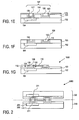
- Figure 1 (g) Some embodiments of a structure according to the present invention are shown in Figure 1 (g) and Figure 2 .
- FIG. 1 (g) An embodiment of a structure 1000 that includes a plug 135 on a substrate 100 is shown in Figure 1 (g) .
- the plug 135 may form a raised contact to permit input of a signal to, or output of a signal from, a bond pad 104 connected to an active area of a device in an underlying layer 102 of the substrate 100.
- FIG. 2 An embodiment of a structure 2000 that includes two interconnected substrates 210, 220 according to the present invention is shown in Figure 2 .
- the structure 2000 includes a first raised contact 211 for a first substrate 210 that is interconnected to a second raised contact 221 for a second substrate 220.
- the raised contact 211 permits input of a signal to, or output of a signal from, a bond pad 204 connected to an active area of a device in an underlying layer 202 of the substrate 210.
- a substrate 100 may include a wafer having multiple chips, or a chip having multiple die, or a die having multiple devices.
- the substrate 100 may be integrated with a package. Interposers may be used in some cases.
- the substrate 100 typically includes an underlying layer 102.
- the underlying layer 102 includes a bond pad 104 that permits input of a signal to or output of a signal from an active area of a device.
- the device may be active or passive.
- the bond pad 104 may be formed from an electrically conductive material having a thickness selected from the range of about 2,500.0-12,000.0 Angstroms.
- the electrically conductive material may include a metal, such as Aluminum or Copper.
- the underlying layer 102 may be covered with an insulator 103 formed from an electrically insulating material having a thickness selected from the range of about 5,000.0-24,000.0 Angstroms.
- the dielectric constant (k) of an electrically insulating material may be determined using capacitance measurements on parallel plate electrical structures.
- the electrically insulating material may include Silicon Oxide having k with a value of about 3.9-4.2.
- an undoped Silica glass (USG) may be used for a device with design rules of about 250 nanometers (nm).
- a tool that may be used to form the insulator 103 includes an Ultima XTM system from Applied Materials.
- the insulator 103 may serve as an interlevel, or interlayer, dielectric (ILD) to separate the bond pad 104 from other electrically conductive materials that may be present in the same or in different levels or layers of the underlying layer 102. Excessive capacitance between nearby electrically conductive lines may degrade the performance of the devices in the underlying layer 102 to which the lines are connected. When the devices include transistors, interline capacitance may contribute to cross-talk and increase the resistance-capacitance (RC) product delay during operation of the transistors, thus degrading their switching speeds.
- ILD interlevel, or interlayer, dielectric
- Interline capacitance in the wiring of the substrate 100 may be reduced by using a low-k material for the insulator 103 between the electrically conductive materials.
- Low-k refers to a value of k that is lower than the value of k of Silicon Oxide.
- Silicon Oxide may be doped with Fluorine to form a Fluorinated Silicate glass (FSG or SiOF), having k with a value of about 3.3-3.7.
- FSG and Silicon Oxide possess many similar properties so process integration is relatively straightforward.
- a low-k dielectric may include organic materials, silicate materials, or a hybrid of both organic and silicate materials, such as organosilicate glass (OSG).
- OSG organosilicate glass
- Silicon Oxide may be doped with Methyl (-CH 3 ) groups to form a Carbon-doped Silicon Oxide (CDO or SiOC) having k with a value of about 2.4-3.3.
- the insulator 103 may be formed from a low-k material having an ultra-low k.
- Ultra-low k refers to a value of k that is lower than about 2.2.
- the insulator 103 may be formed from a material having k with a value below about 1.5.
- Materials with an ultra-low k are usually porous and may include aerogels and xerogels.
- the low-k or ultra-low k material may require the use of a barrier layer to prevent diffusion, intermixing, or reaction with other materials.
- a capping layer such as Silicon Nitride (SiN) or Silicon Oxynitride (SiON), may be formed over the low-k or ultra-low k material.
- the insulator 103 may be formed using a chemical vapor deposition (CVD) process.
- a low-k material that may be formed using a plasma-enhanced CVD (PECVD) process includes Black DiamondTM (a CDO having k with a value of about 2.4-3.1) from Applied Materials, CORALTM (a CDO having k with a value of about 2.4-2.8) from Novellus Systems, and Flowfill® (a CDO having k with a value of about 2.5-2.8) from Trikon Technologies.
- An ultra-low k material that may be formed using PECVD includes OrionTM (a CDO having k with a value of about 2.0-2.2) from Trikon Technologies.
- a tool that may be used to form the low-k or ultra-low k material includes a Producer® system from Applied Materials.
- a SEQUEL ExpressTM system or a VECTORTM system from Novellus Systems may also be used.
- the insulator 103 may be formed from a spin-on dielectric (SOD).
- SOD spin-on dielectric
- the SOD may require the use of an adhesion layer.
- Low-k materials that may be formed using a spin-on process from a liquid source include SiLKTM (an aromatic hydrocarbon polymer having k with a value of about 2.65) from Dow Chemical and HOSPTM (a hybrid organic-siloxane polymer or OSG having k with a value of about 2.5) from Honeywell Electronic Materials (HEM).
- An ultra-low k material that may be spun-on includes NANOGLASS® (a porous Silica having k with a value of about 1.3-2.2) from HEM.
- a tool that may be used to form the low-k or ultra-low k material includes a spin track from Tokyo Electron Ltd. (TEL).
- a mask is defined in a radiation-sensitive material called photoresist 101 by a photolithography process.
- the photoresist 101 is applied over the insulator 103 of the substrate 100.
- a feature 99 is patterned in the photoresist 101 by exposure to radiation of the appropriate wavelength and dose, as modulated by a reticle, followed by development to form the mask.
- the exposure may be done in an imaging tool, such as a stepper or a scanner.
- the feature 99 in the photoresist 101 mask may then be transferred into an opening 105 in the insulator 103 by an etch process.
- the etch process to form the opening 105 may include a plasma etch process or a reactive ion etch process (RIE).
- RIE reactive ion etch process
- the opening 105 uncovers a portion of the bond pad 104 of the device in the underlying layer 102, as shown in an embodiment in Figure 1 (b) .
- the opening 105 may include a shape derived from the reticle, such as a via, a trench, or a trench overlying a via.
- the opening 105 may have a vertical dimension, or depth, of greater than about 1.00 micron (um) and a lateral dimension, such as a width, of less than about 0.10 um. High directionality is desired for the etch when the opening 105 has an aspect ratio (depth : width) of about 6:1 or greater.
- a high density plasma such as an inductively-coupled Radio Frequency (RF) plasma (ICP), may be used.
- RF Radio Frequency
- the etch to form the opening 105 may be performed with a gas mixture.
- the gas mixture may include an etching gas, such as CF 4 , and a polymerizing gas, such as CH 2 F 2 .
- the etching gas is the principal source of Fluorine for etching the insulator 103 while the polymerizing gas passivates the sidewalls of the opening 105 to improve selectivity.
- gases that may be used include CHF 3 and C 3 F 6 .
- the etch rate of the insulator 103 may be about 1,500.0-12,000.0 Angstroms per minute.
- a tool that may be used to form the opening 105 includes an Omega® MORITM system from Trikon Technologies. If desired, the etch of the insulator 103, the removal of any underlying barrier layer or etch stop layer, and the strip of the photoresist 101 may be done sequentially in an integrated tool such as an Exelan® system from Lam Research or an eMaxTM EnTekTM Centura® system from Applied Materials.
- the etch selectivity of the insulator 103 to a photoresist 101 mask may be about 2:1 to 7:1. If etch selectivity of the insulator 103 to the photoresist 101 mask is too low, an intermediate mask, called a hard mask, may be included between the insulator 103 and the photoresist 101. In such a case, a first etch process is used to transfer a first feature 99 that is patterned in the photoresist 101 into a second feature in the hard mask. Then, a second etch process transfers the second feature from the hard mask into the opening 105 in the insulator 103. The etch selectivity of the insulator 103 to the hard mask may be higher than about 20:1.
- a hard mask process may include a material such as SiN or SiON. In one embodiment, a stack including two or more hard masks may be used.
- a buried etch stop (BES) layer may be included between the bond pad 104 and the insulator 103.
- the etch stop layer may include SiN or Silicon Carbide (SiC).
- SiN has a k with a value of 6.5, which is relatively high, so an alternative material, such as BLOkTM from Applied Materials having a k with a value of about 4.5-5.0, may be used.
- BLOkTM Silicon Carbide
- an etch stop layer having a k with an even lower value may be used to minimize the capacitance of the overall dielectric stack structure.
- An example is HOSP BEStTM from HEM which has a k with a value of about 2.6.
- a barrier layer 115 may be needed to protect the insulator 103 and the underlying layer 102, including the bond pad 104.
- the high diffusivity of Copper and the presence of mid-gap states in Copper make a barrier layer 115 necessary. Otherwise, Copper may diffuse into the insulator 103 or underlying layer 102 and degrade the carrier lifetime of a semiconductor material such as Silicon.
- a barrier layer 115 is formed over the insulator 103 and in the opening 105.
- the barrier layer 115 may have a thickness selected from the range of about 50.0-600.0 Angstroms.
- the barrier layer 115 should provide good coverage both inside and outside the opening 105. In some cases, the thickness of the barrier layer 115 inside the opening may be different from the thickness of the barrier layer 115 outside the opening.
- the barrier layer 115 should effectively block diffusion from the seed layer 120 or a conductor 130 into the insulator 103 or underlying layer 102. Serving as an underlayer or liner, the barrier layer 115 should be capable of good adhesion to the seed layer 120, the conductor 130, the insulator 103, and the underlying layer 102, including the bond pad 104. However, the barrier layer 115 should also have minimal interaction, such as chemical or electrochemical reaction, with the seed layer 120, the conductor 130, the insulator 103, or the underlying layer 102, including the bond pad 104.
- the barrier layer 115 may be formed from a metal, including a refractive metal, such as Tantalum (Ta), or an alloy, such as Titanium-Tungsten (TiW), or a ceramic, such as Tantalum-Nitride (TaN), Tantalum-Silicon-Nitride (TaSiN), Titanium-Nitride (TiN), or Tungsten-Nitride (WN).
- a refractive metal such as Tantalum (Ta)
- TiW Titanium-Tungsten
- TiW Titanium-Tungsten
- WN Tungsten-Nitride
- the barrier layer 115 may include a lower layer of TaN to adhere to the underlying insulator 103 and an upper layer of Ta to adhere to the overlying seed layer 120.
- a bilayer may have a total thickness of about 150.0-350.0 Angstroms.
- I-PVD ionized physical vapor deposition
- LTS long-throw sputtering
- a tool that may be used for I-PVD include an INOVATM system from Novellus Systems, a Sigma® system from Trikon Technologies, and an Entron system from Ulvac Technologies.
- MOCVD metal-organic CVD
- the precursors used in MOCVD react on the exposed surfaces of the opening 105, rather than in the gas phase as in CVD, so coverage is usually good.
- a tool that may be used for MOCVD includes a NEXUSTM system from Veeco Instruments.
- the barrier layer 115 may be formed using atomic layer deposition (ALD) when a thickness of about 100.0 Angstroms or less is desired.
- ALD atomic layer deposition
- ALD can provide good step coverage and good uniformity even while permitting the use of a low deposition temperature of about 200.0-400.0 degrees Centigrade.
- a tool that may be used for ALD includes a NEXUSTM system from Veeco Instruments or a LYNX2® or LYNX3TM system from Genus.
- a seed layer 120 is first formed over the barrier layer 115, as shown in an embodiment in Figure 1 (c) .
- the seed layer 120 In order to serve as a base for electroplating, the seed layer 120 must be electrically conductive and continuous over the barrier layer 115. Adhesion loss of the seed layer 120 or interfacial reaction with the barrier layer 115 should be prevented.
- the seed layer 120 may include a metal, such as Copper, or an alloy.
- the seed layer 120 typically has a thickness selected from a range of about 20.0-2,500.0 Angstroms.
- the seed layer 120 may be deposited by I-PVD, especially when the conductor 130 is to be subsequently formed by electroplating. If desired, the barrier layer 115 and the seed layer 120 may be sequentially deposited under vacuum in a tool such as an Endura® ElectraTM system from Applied Materials.
- the conductor 130 When the conductor 130 is to be subsequently formed by PVD, better material properties and surface characteristics may be achieved for the conductor 130 if the seed layer 120 is formed using CVD.
- the seed layer 120 may also be formed with ALD or electroless plating.
- a conductor 130 is formed over the seed layer 120, as shown in an embodiment in Figure 1 (d) .
- the conductor 130 includes a material that is electrically conductive.
- the seed layer 120 and the conductor 130 may be formed from the same material or from different materials.
- the conductor 130 should fill the opening 105 from the bottom up. When completely filled, the opening 105 should not have defects, such as voids, seams, or cracks. Adhesion loss of the conductor 130 or interfacial reaction with the seed layer 120 should be prevented.
- the conductor 130 may include a metal, such as Copper, or an alloy.
- the conductor 130 typically has a thickness of about 0.2-2.8 um.
- Advantages of Copper compared with Aluminum include higher intrinsic conductivity, lower susceptibility to electromigration, and better filling of an opening 105 that has an aspect ratio (height : width) of about 3:1 or greater.
- Disadvantages of Copper compared with Aluminum include difficulty of etching with a RIE process, vulnerability to corrosion, and a high diffusion rate in Silicon.
- the conductor 130 may be formed by an electrochemical process, such as electroplating. Electroplating of the conductor 130 may be performed in a bath or a solution containing ions of the material to be deposited.
- the seed layer 120 acts as a negative electrode of an electrochemical cell. Electroplating may be carried out in the solution using a constant current, a constant voltage, or variable waveforms of current or voltage, depending on the thickness and the film properties that are desired. When current is turned on, positive ions in the electroplating solution combine with electrons produced at the surface of the seed layer 120. The ions are thus chemically reduced to atoms which form the conductor 130 over the seed layer 120.
- a tool that may be used for electroplating includes an Electra CuTM system from Applied Materials, a SABRETM Electrofill system from Novellus Systems, and a ParagonTM system from SEMITOOL.
- Successful electroplating of the conductor 130 may require the use of various additives that are surface active.
- the additives to the electroplating solution are usually organic and may include functional groups of Sulfur or Nitrogen. Correct filling of an opening 105 having a large aspect ratio may require the proper balance of inhibitors (suppressors) and accelerators in the electroplating solution. Otherwise, defects, such as voids, seams, and cracks, may form within the conductor 130 and be uncovered later during planarization. Good thickness uniformity from substrate-to-substrate and smooth surface finish of the conductor 130 may also require the use of levelers and brighteners in the electroplating solution.
- the concentrations of various ions, such as Copper, Chloride, and Hydrogen, in the electroplating solution may be adjusted in response to the monitoring of parameters, such as pH, conductivity, and the absorbance in the visible portion of the electromagnetic spectrum.
- Cyclic Voltammetric Stripping (CVS) analysis may be used to measure the concentration of the additives in the electroplating solution.
- the conductor 130 may be formed with a PVD process or a CVD process, sometimes without first forming the seed layer 120.
- a PVD process or a CVD process may be particularly advantageous when filling an opening 105 that has an aspect ratio (height: width) of about 6:1 or greater.
- a MOCVD process may also be used.
- a treatment may be used to modify material properties or surface characteristics of the conductor 130.
- the treatment of the conductor 130 may include a rapid thermal anneal (RTA) process after deposition to modify or stabilize the grain size of the conductor 130.
- RTA rapid thermal anneal
- Copper that has been formed by electroplating may have a grain size of about 0.1-1.0 millimeter (mm), depending on the thickness, deposition conditions, and anneal conditions.
- a larger grain size in the conductor 130 usually corresponds to a lower resistivity.
- Copper may have a resistivity of about 1.0-4.0 micro-ohm-centimeter.
- a raised contact for the substrate 100 is formed by planarizing the conductor 130 to form a plug 135, followed by recessing the insulator 103 around the plug 135.
- a chemical-mechanical polishing (CMP) process which combines abrasion (mechanical forces) and dissolution (chemical or electrochemical reactions), may be optimized to either planarize or to recess different materials.
- the substrate 100 may be held in a carrier attached to a head of a CMP system.
- a pad may be attached to a table or a platen of the CMP system. When the head and the platen are moved, the pad may apply mechanical forces to the conductor 130 on the substrate 100.
- the motion of the head and the motion of the platen may be rotary, orbital, or linear. Alternatively, the pad may be moved with respect to the platen, such as with a polishing belt.
- a slurry may be dispensed on the pad to produce chemical reactions with the conductor 130 on the substrate 100. Abrasives in the slurry may also apply mechanical forces to the conductor 130 on the substrate 100 in conjunction with the pad.
- polish selectivity may be adjusted by changing the polish rates for different materials.
- Polish selectivity may be optimized by changing the properties of the polish pad (such as hardness, stiffness, abrasiveness, porosity, and layout of grooves or channels), the properties of the polish slurry (such as chemical composition, chemical concentration, pH, abrasive type, abrasive quantity, and abrasive particle size distribution), and the parameters of the polish system (such as down force or pressure of the carrier relative to the platen, linear velocity of the carrier relative to the platen, slurry flowrate, and platen temperature).
- properties of the polish pad such as hardness, stiffness, abrasiveness, porosity, and layout of grooves or channels
- the properties of the polish slurry such as chemical composition, chemical concentration, pH, abrasive type, abrasive quantity, and abrasive particle size distribution
- parameters of the polish system such as down force or pressure of the carrier relative to the platen, linear velocity of the carrier relative to the plate
- the critical process parameters for a CMP process may be monitored across the substrate 100 with appropriate sensors.
- the process parameters may then be controlled by adjusting the related equipment parameters with appropriate actuators.
- the CMP system may include a control unit, including a computer, and an operator interface.
- closed loop control of the CMP process and equipment may be implemented.
- a closed loop may involve feedforward or feedback control using one or more of the following control methods: proportional, differential, or integral.
- a metrology tool may be integrated with a CMP tool.
- the optical consequences of dishing and erosion may be measured with a tool, including a NovaScan system from Nova Measuring Instruments or a NanoSpec® system from NanoMetrics.
- a stand-alone tool used for CMP includes a Mirra® system from Applied Materials.
- an integrated tool such as a Mirra MesaTM or a ReflexionTM system from Applied Materials or a TeresTM system from Lam Research may be used.
- An integrated tool may combine CMP with related process steps, such as a pre-clean and a post-clean to result in dry in/dry out of the substrate 100.
- Consumables for CMP including pads and slurries, may be obtained from various sources, such as Rodel and Cabot.
- a combination of a first CMP process and a second CMP process is used to form a raised contact for a substrate 100.
- the first CMP process performs the planarization while the second CMP process performs the recessing.
- the first CMP process has a high polish selectivity for the conductor 130 relative to the underlying barrier layer 115.
- the first CMP process may remove the conductor 130 across the substrate 100 and uncover the upper surface 108 of the barrier layer 115, as shown in an embodiment in Figure 1 (e) .
- the barrier layer 115 may serve as a polish stop layer since the conductor 130 is usually softer.
- a polish stop layer improves planarization by reducing any large or non-uniform topography that exists across the substrate 100.
- a suitable slurry may be selected to accomplish a high polish selectivity for the conductor 130 relative to the barrier layer 115.
- the polish selectivity of the conductor 130 to the barrier layer 115 may have an average value of about 50:1-250:1.
- a higher polish selectivity allows the use of a thinner barrier layer 115.
- a thinner barrier layer 115 will result in a smaller increase in the resistance between the bond pad 104 and the conductor 130.
- the slurry may include an abrasive, such as Alumina or Silica, an oxidizer, such as Hydrogen Peroxide (H 2 O 2 ), a passivating or film-forming agent (corrosion inhibitor), such as Benzotriazole (BTA), and a complexing agent which may be an amino acid, such as Glycine, or an organic acid/salt system, such as Citric Acid/Potassium Citrate.
- an abrasive such as Alumina or Silica
- an oxidizer such as Hydrogen Peroxide (H 2 O 2 )
- a passivating or film-forming agent (corrosion inhibitor) such as Benzotriazole (BTA)
- BTA Benzotriazole
- a complexing agent which may be an amino acid, such as Glycine, or an organic acid/salt system, such as Citric Acid/Potassium Citrate.
- Typical parameters for the first CMP process to planarize the conductor 130 include a slurry pH of about 5.0-9.0, a slurry flowrate of about 100.0-350.0 milliliters per minute, a platen rotation of about 15.0-100.0 revolutions per minute (rpm), a carrier rotation of about 15.0-100.0 rpm, and a polish pressure of about 1.0-7.0 pounds per square inch (psi).
- the removal rate for the conductor 130 may be about 1,000.0-14,000.0 Angstroms per minute.
- the first CMP process includes two or more steps.
- a first step having a higher removal rate, is used to remove most of the overburden of the conductor 130.
- the first step may be a timed polish or may be controlled by in situ monitoring of a parameter, such as thickness or eddy current.
- a second step having a lower removal rate, such as about 1,000.0-2,500.0 Angstroms per minute, is used to clear the conductor 130 to uncover the upper surface 108 of the barrier layer 115 without breaking through to the insulator 103.
- the second step may be a timed polish or an endpoint polish.
- the second step may include an overpolish time or an overpolish percentage, such as 15.0%, after detection of endpoint on the barrier layer 115. If desired, each step may be done on a separate platen or on a separate CMP system.
- the plug includes conductor 130, seed layer 120, and barrier layer 115.
- the shape of the plug 135 is influenced by the shape of the opening 105.
- the plug 135 may be a post or a stud if the opening 105 is a via.
- the plug 135 may be a line if the opening 105 is a trench.
- An undesirable topographical change that may result from the first CMP process is dishing of the plug 135. Dishing creates a depression in the upper surface 107 of the conductor 130 within the plug 135 (inside the opening 105) relative to the surrounding insulator 103 (outside the opening 105).
- Dishing may be more severe for a plug 135 with a larger lateral dimension.
- Proper optimization of the first CMP process will produce a first polished upper surface 107 of the plug that is approximately flat and level with the upper surface 108 of the barrier layer 115 that has been exposed, as shown in an embodiment in Figure 1 (e) .
- Another undesirable topographical change that may result from the first CMP process is erosion of the material in the spaces between plugs within a cluster or array 137 of plugs relative to the material in the field region far away from the cluster or array 137 of plugs.
- Erosion creates a depression in the spaces between plugs (within the cluster or array 137) relative to material in the field region (outside the cluster or array 137). Erosion may result in the partial or complete removal of the barrier layer 115 in the spaces between the plugs. In areas where the barrier layer 115 has been removed, erosion may further result in removal of some of the underlying insulator 103 in the spaces between the plugs.
- Erosion may be more severe for a cluster or array 137 having densely-packed plugs with small spaces between the plugs.
- Proper optimization of the first CMP process will minimize the difference between the removal rate of material in the spaces between plugs within a cluster or array 137 of plugs and the removal rate of material outside the cluster or array 137 of plugs.
- a second CMP process is used to remove the barrier layer 115 outside the opening 105 and recess the uncovered portion of the insulator 103 below the upper surface 109 of the plug 135, as shown in an embodiment in Figure 1 (g) .
- the barrier layer 115 may also be removed from a portion of the sidewalls of the plug 135.
- the structure 1000 includes a plug 135 for a substrate 100.
- the plug 135 may form a raised contact to permit input of a signal to, or output of a signal from, a bond pad 104 connected to an active area of a device in an underlying layer 102 of the substrate 100.
- a suitable slurry may be selected to accomplish a high polish selectivity for both the barrier layer 115 and the insulator 103 relative to the conductor 130.
- the polish selectivity of the insulator 103 to the conductor 130 may have an average value of about 5:1 or greater.
- the slurry may include an abrasive, such as Silica, and a complexing agent.
- the complexing agent may be Ammonium Hydroxide (NH 4 OH) or an organic acid/salt system, such as Citric Acid/Potassium Citrate.
- a biocide may also be included.
- a relatively soft pad is used to minimize the removal of the conductor 130 and to prevent the generation of defects.
- Typical parameters for the second CMP process to recess the insulator 103 include a slurry pH of about 6.0-12.0, a slurry flowrate of about 100.0-350.0 milliliters per minute, a platen rotation of about 5.0-85.0 rpm, a carrier rotation of about 5.0-85.0 rpm, and a polish pressure of about 1.0-7.0 psi.
- the linear velocity of the platen may be about 20.0-350.0 feet per minute.
- the slurry pH may be about 9.0-11.0
- the polish pressure may be about 4.0-6.0 psi
- the linear velocity of the platen may be about 20.0-140.0 feet per minute.
- the second CMP process may be modified to avoid fracturing or delaminating the low-k material forming the insulator 103.
- the second CMP process may be followed by a post-clean, such as a scrub, in a non-oxidizing environment with an organic acid or organic acid buffer.
- a post-clean such as a scrub
- the pH may be selected from the range of about 2.0-6.0.
- the insulator 103 as shown in Figure 1 (f) instead of the barrier layer 115 as shown in Figure 1 (e) , may serve as a polish stop layer when using CMP to planarize the conductor 130 to form the plug 135. Then, the insulator 103 may be recessed directly to form the raised contact for the substrate 100.
- the slurry chemistry and the polish conditions and parameters may have to be optimized to achieve the desired polish selectivities and polish removal rates.
- the recessing rate of the insulator 103 may be about 300.0-2,500.0 Angstroms per minute in the field region far away from the cluster or array 137 of plugs.
- the interior upper surface 110 of the insulator 103 may differ in height from the exterior upper surface 112 of the insulator 103.
- Interior refers to a location within a cluster or array 137 of plugs.
- Exterior refers to a location outside the cluster or array 137 of plugs. In most cases, the interior upper surface 110 of the insulator 103 is higher than the exterior upper surface 112 of the insulator 103.
- Recessing the insulator 103 with the second CMP process may reduce the thickness of the conductor 130.
- the difference in height between the first polished upper surface 107 of the plug and the second polished upper surface 109 of the plug 135 corresponds to conductor 130 thinning.
- Conductor 130 thinning should be avoided except to the extent needed to planarize the upper surface 107 of the plugs in the cluster or array 137 of plugs.
- the plug relief 122 is the amount of protrusion of the second polished upper surface 109 of the plug 135 relative to the interior upper surface 110 of the insulator 103.
- Interior refers to a location within a cluster or array 137 of plugs.
- the step height 124 is the amount of protrusion of the second polished upper surface 109 of the plug 135 relative to the exterior upper surface 112 of the insulator 103.
- Exterior refers to a location outside the cluster or array 137 of plugs.
- the field region includes the exterior locations that are far away from the cluster or array 137 of plugs.
- the oxide relief is the difference between the step height 124 and the plug relief 122.
- the plug relief 122 and the step height 124 may be affected by a variety of factors, including the local pattern density (the spacing between plugs within each cluster or array 137 of plugs) and the global pattern density (the spacing between separate clusters or arrays 137 of plugs across the substrate 100). In general, narrower plugs 135 and narrower spaces between plugs 135 decreases the thinning of the conductor 130 and produces a smaller plug relief 122.
- the plug relief 122 and the step height 124 may be measured and visualized with an atomic force microscope (AFM) or a high-resolution profilometer (HRP).
- a tool such as a DimensionTM system from Veeco Instruments, may be used.
- the nominal value for the plug relief 122 may be selected from the range of about 300.0-3,200.0 Angstroms while the nominal value for the step height 124 may be selected from the range of about 400.0-5,700.0 Angstroms.
- the plug relief 122 may be about 700.0-2,200 Angstroms, with a range across the substrate 100 of less than 8.0 % while the step height 124 may be about 1,100.0-3,800.0 Angstroms, with a range across the substrate 100 of less than about 12.0 %.
- the plug relief 122 should be controlled more tightly than the step height 124.
- the step height 124 should not be more than about 50.0 % of the original thickness of the insulator 103.
- defect inspection may be done.
- a tool such as an AIT system from KLA-Tencor may be used.
- SEM scanning electron microscope
- a tool that may be used includes a SEMVisionTM system from Applied Materials.
- Automated defect classification (ADC) may be provided by post-processing software.
- Defects discovered after performing CMP may not be directly caused by the CMP process. Instead, some defects may have arisen from an earlier process, such as during formation of the insulator 103, the opening 105, the barrier layer 115, the seed layer 120, or the conductor 130.
- the protruding plug may be used to form a raised contact for a substrate.
- a first raised contact 211 for a first substrate 210 may be interconnected to a second raised contact 221 for a second substrate 220, as shown in an embodiment in Figure 2 .
- the structure 2000 includes a first raised contact 211 for a first substrate 210 that is interconnected to a second raised contact 221 for a second substrate 220.
- the raised contact 211 permits input of a signal to, or output of a signal from, a bond pad 204 connected to an active area of a device in an underlying layer 202 of the substrate 210.
- the interconnection between the raised contacts 211, 221 of two or more substrates 210, 221 may be degraded by topographical changes.
- Such undesirable topographical changes may be caused by dishing, erosion, or conductor 130 thinning.
- the topographical consequences of dishing and erosion may be measured and visualized with an AFM or an HRP.
- a tool such as a DimensionTM system from Veeco Instruments may be used.
- the topographical consequences of surface roughness and uncovered defects, such as residues, scratches, and voids, may also be measured.
- the nominal value and uniformity of plug relief 122 and step height 124 across the substrate 100 may be affected by erosion. Erosion may be minimized by adding dummy plugs outside the cluster or array 137 of plugs.
- the dummy plugs may differ from the functional plugs (in the raised contacts 211, 221) in size, shape, or layout. In one embodiment, the dummy plugs are wider than the functional plugs (in the raised contacts 211, 221) so that the height of the dummy plugs may be reduced intentionally by dishing.
- Clusters or arrays 137 of dummy plugs may be strategically inserted at certain locations in the field region to modify and control the recession of the insulator 103 across the substrate 100.
- the locations of the dummy plugs may depend on various parameters, including the dimensions (such as length, width, thickness) of the substrate 100, the flatness of the substrate 100, the co-planarity of the substrate 100, and the locations of the functional plugs (in the raised contacts 211, 221).
- the dummy plugs are only included with the functional plugs (in the raised contacts 211, 221) in the final (top) layer of the substrate 100.
- the dummy plugs are connected to other structures and features in one or more underlying layers of the substrate 100 to create the desired topography.
- dummy plugs included in two or more layers may be stacked vertically. Dummy plugs, that would otherwise float electrically, may be grounded to prevent parasitic capacitance during operation of the device in the underlying layer 102.
Landscapes
- Internal Circuitry In Semiconductor Integrated Circuit Devices (AREA)
- Printing Elements For Providing Electric Connections Between Printed Circuits (AREA)
Abstract
Description
- The present invention relates to the field of semiconductor integrated circuit (IC) manufacturing, and more specifically, to a method of forming raised contacts for a substrate.
- In 1965, Gordon Moore first observed that the number of transistors per unit area on a chip appeared to double approximately every 18 months. Ever since then, the semiconductor industry has managed to introduce new designs and processes on schedule to deliver the improvement in device density projected by the so-called Moore's Law. In particular, major enhancements in optics and photolithography have reduced the critical dimension (CD) that can be successfully patterned in the features on a chip or other substrate. At the same time, significant improvements in doping, deposition, and etch have decreased the concentration, depth, and thickness that can be precisely achieved across the substrate.
- As device dimensions approach atomic dimensions, the fundamental limitations of physics will play increasingly larger roles in determining the performance and reliability of the devices on the substrate. In the past, issues of scaling have generally involved either the transistor in the front-end of semiconductor processing or the wiring in the back-end of semiconductor processing. However, it is becoming increasingly important to balance the scaling of the transistor and the interconnect on the substrate with the scaling of the interconnection between multiple substrates.
- Thus, what is needed is a method of forming raised contacts for interconnection between substrates and a structure having such raised contacts.
-
US 20020003307 A1 discloses a semiconductor device and method for fabricating the device. By polishing according to the CMP method, a through hole conductor and a grounding wiring layer, which are made of copper become concave in a dish-like shape and lowered in level causing a dishing portion since they have a hardness lower than that of a through hole insulator made of silicon nitrite. The through hole insulator is selectively etched by a reactive ion etching method until the through hole insulator comes to have a height equal to the height of a bottom portion of the dishing portion of the through hole conductor. -
US 20010008311A1 discloses a semiconductor device and method for fabricating the same and an apparatus for chemical mechanical polishing and a method of chemical mechanical polishing. -
US 6194313 discloses a method for reducing recesses for the formation of a local interconnect and/or plug trench fill for an etch back process. -
US 5985748 discloses a method of making a semiconductor device using chemical-mechanical polishing having a combination-step process. - The inventive method is defined in claim 1.
-
-
Figures 1 (a) -(g) are illustrations of a cross-sectional view of various embodiments of a method of forming a raised contact for a substrate according to the present invention. -
Figure 1 (g) is also an illustration of a cross-sectional view of a structure that includes a plug on a substrate according to the present invention. -
Figure 2 is an illustration of a cross-sectional view of an embodiment of a method of interconnecting raised contacts between substrates according to the present invention. -
Figure 2 is also an illustration of a cross-sectional view of a structure that includes two substrates interconnected with raised contacts according to the present invention. - In the following description, numerous details, such as specific materials, dimensions, and processes, are set forth in order to provide a thorough understanding of the present invention. However, one skilled in the art will realize that the invention may be practiced without these particular details. In other instances, well-known semiconductor equipment and processes have not been described in particular detail so as to avoid obscuring the present invention.
- A device may be formed on a substrate by iteratively performing some combination of unit processes such as doping, depositing, patterning, and etching. During the fabrication of integrated circuits (ICs) on a chip or substrate, transistors may be formed in semiconductor material and separated by an electrically insulating material. The transistors may then be wired up with an interconnect system that has multiple layers of an electrically conductive material separated by the electrically insulating material.
- A higher device density per unit volume may be achieved by stacking two or more substrates. The substrates may be wired with 3-dimensional interconnects. The 3-dimensional interconnects may involve raised contacts on the substrates. The present invention describes a method of forming raised contacts for interconnection between substrates.
- Some embodiments of a structure according to the present invention are shown in
Figure 1 (g) and Figure 2 . - An embodiment of a
structure 1000 that includes aplug 135 on asubstrate 100 is shown inFigure 1 (g) . Theplug 135 may form a raised contact to permit input of a signal to, or output of a signal from, abond pad 104 connected to an active area of a device in anunderlying layer 102 of thesubstrate 100. - An embodiment of a
structure 2000 that includes twointerconnected substrates Figure 2 . Thestructure 2000 includes a first raisedcontact 211 for afirst substrate 210 that is interconnected to a second raisedcontact 221 for asecond substrate 220. In one embodiment, the raisedcontact 211 permits input of a signal to, or output of a signal from, abond pad 204 connected to an active area of a device in anunderlying layer 202 of thesubstrate 210. - Various embodiments of a method of forming raised contacts for a
substrate 100 according to the present invention are shown inFigures 1 (a) -(g) andFigure 2 . Asubstrate 100 may include a wafer having multiple chips, or a chip having multiple die, or a die having multiple devices. - The
substrate 100 may be integrated with a package. Interposers may be used in some cases. Thesubstrate 100 typically includes anunderlying layer 102. Theunderlying layer 102 includes abond pad 104 that permits input of a signal to or output of a signal from an active area of a device. The device may be active or passive. Thebond pad 104 may be formed from an electrically conductive material having a thickness selected from the range of about 2,500.0-12,000.0 Angstroms. The electrically conductive material may include a metal, such as Aluminum or Copper. - The
underlying layer 102 may be covered with aninsulator 103 formed from an electrically insulating material having a thickness selected from the range of about 5,000.0-24,000.0 Angstroms. The dielectric constant (k) of an electrically insulating material may be determined using capacitance measurements on parallel plate electrical structures. The electrically insulating material may include Silicon Oxide having k with a value of about 3.9-4.2. In one embodiment, an undoped Silica glass (USG) may be used for a device with design rules of about 250 nanometers (nm). A tool that may be used to form theinsulator 103 includes an Ultima X™ system from Applied Materials. - The
insulator 103 may serve as an interlevel, or interlayer, dielectric (ILD) to separate thebond pad 104 from other electrically conductive materials that may be present in the same or in different levels or layers of theunderlying layer 102. Excessive capacitance between nearby electrically conductive lines may degrade the performance of the devices in theunderlying layer 102 to which the lines are connected. When the devices include transistors, interline capacitance may contribute to cross-talk and increase the resistance-capacitance (RC) product delay during operation of the transistors, thus degrading their switching speeds. - Interline capacitance in the wiring of the
substrate 100 may be reduced by using a low-k material for theinsulator 103 between the electrically conductive materials. Low-k refers to a value of k that is lower than the value of k of Silicon Oxide. For a device with design rules of about 180 nm, Silicon Oxide may be doped with Fluorine to form a Fluorinated Silicate glass (FSG or SiOF), having k with a value of about 3.3-3.7. FSG and Silicon Oxide possess many similar properties so process integration is relatively straightforward. - The value of k of FSG is not low enough for devices with smaller design rules so other low-k materials have to be used. A low-k dielectric may include organic materials, silicate materials, or a hybrid of both organic and silicate materials, such as organosilicate glass (OSG). For a device with design rules of about 130 nm, Silicon Oxide may be doped with Methyl (-CH3) groups to form a Carbon-doped Silicon Oxide (CDO or SiOC) having k with a value of about 2.4-3.3.
- For a device with design rules of about 90 nm, the
insulator 103 may be formed from a low-k material having an ultra-low k. Ultra-low k refers to a value of k that is lower than about 2.2. For a device with design rules of about 70 nm down to about 50 nm, theinsulator 103 may be formed from a material having k with a value below about 1.5. Materials with an ultra-low k are usually porous and may include aerogels and xerogels. In some cases, the low-k or ultra-low k material may require the use of a barrier layer to prevent diffusion, intermixing, or reaction with other materials. In one embodiment, a capping layer, such as Silicon Nitride (SiN) or Silicon Oxynitride (SiON), may be formed over the low-k or ultra-low k material. - The
insulator 103 may be formed using a chemical vapor deposition (CVD) process. A low-k material that may be formed using a plasma-enhanced CVD (PECVD) process includes Black Diamond™ (a CDO having k with a value of about 2.4-3.1) from Applied Materials, CORAL™ (a CDO having k with a value of about 2.4-2.8) from Novellus Systems, and Flowfill® (a CDO having k with a value of about 2.5-2.8) from Trikon Technologies. An ultra-low k material that may be formed using PECVD includes Orion™ (a CDO having k with a value of about 2.0-2.2) from Trikon Technologies. A tool that may be used to form the low-k or ultra-low k material includes a Producer® system from Applied Materials. A SEQUEL Express™ system or a VECTOR™ system from Novellus Systems may also be used. - Alternatively, the
insulator 103 may be formed from a spin-on dielectric (SOD). In some cases, the SOD may require the use of an adhesion layer. Low-k materials that may be formed using a spin-on process from a liquid source include SiLK™ (an aromatic hydrocarbon polymer having k with a value of about 2.65) from Dow Chemical and HOSP™ (a hybrid organic-siloxane polymer or OSG having k with a value of about 2.5) from Honeywell Electronic Materials (HEM). An ultra-low k material that may be spun-on includes NANOGLASS® (a porous Silica having k with a value of about 1.3-2.2) from HEM. A tool that may be used to form the low-k or ultra-low k material includes a spin track from Tokyo Electron Ltd. (TEL). - A mask is defined in a radiation-sensitive material called
photoresist 101 by a photolithography process. First, thephotoresist 101 is applied over theinsulator 103 of thesubstrate 100. As shown in an embodiment inFigure 1 (a) , afeature 99 is patterned in thephotoresist 101 by exposure to radiation of the appropriate wavelength and dose, as modulated by a reticle, followed by development to form the mask. The exposure may be done in an imaging tool, such as a stepper or a scanner. - The
feature 99 in thephotoresist 101 mask may then be transferred into anopening 105 in theinsulator 103 by an etch process. The etch process to form theopening 105 may include a plasma etch process or a reactive ion etch process (RIE). Theopening 105 uncovers a portion of thebond pad 104 of the device in theunderlying layer 102, as shown in an embodiment inFigure 1 (b) . - The
opening 105 may include a shape derived from the reticle, such as a via, a trench, or a trench overlying a via. Theopening 105 may have a vertical dimension, or depth, of greater than about 1.00 micron (um) and a lateral dimension, such as a width, of less than about 0.10 um. High directionality is desired for the etch when theopening 105 has an aspect ratio (depth : width) of about 6:1 or greater. In one embodiment, a high density plasma, such as an inductively-coupled Radio Frequency (RF) plasma (ICP), may be used. - The etch to form the
opening 105 may be performed with a gas mixture. The gas mixture may include an etching gas, such as CF4, and a polymerizing gas, such as CH2F2. The etching gas is the principal source of Fluorine for etching theinsulator 103 while the polymerizing gas passivates the sidewalls of theopening 105 to improve selectivity. Other gases that may be used include CHF3 and C3F6. The etch rate of theinsulator 103 may be about 1,500.0-12,000.0 Angstroms per minute. - A tool that may be used to form the
opening 105 includes an Omega® MORI™ system from Trikon Technologies. If desired, the etch of theinsulator 103, the removal of any underlying barrier layer or etch stop layer, and the strip of thephotoresist 101 may be done sequentially in an integrated tool such as an Exelan® system from Lam Research or an eMax™ EnTek™ Centura® system from Applied Materials. - The etch selectivity of the
insulator 103 to aphotoresist 101 mask may be about 2:1 to 7:1. If etch selectivity of theinsulator 103 to thephotoresist 101 mask is too low, an intermediate mask, called a hard mask, may be included between theinsulator 103 and thephotoresist 101. In such a case, a first etch process is used to transfer afirst feature 99 that is patterned in thephotoresist 101 into a second feature in the hard mask. Then, a second etch process transfers the second feature from the hard mask into theopening 105 in theinsulator 103. The etch selectivity of theinsulator 103 to the hard mask may be higher than about 20:1. A hard mask process may include a material such as SiN or SiON. In one embodiment, a stack including two or more hard masks may be used. - If the etch selectivity of the
insulator 103 to theunderlying bond pad 104 is too low, a buried etch stop (BES) layer may be included between thebond pad 104 and theinsulator 103. The etch stop layer may include SiN or Silicon Carbide (SiC). However, SiN has a k with a value of 6.5, which is relatively high, so an alternative material, such as BLOk™ from Applied Materials having a k with a value of about 4.5-5.0, may be used. If desired, an etch stop layer having a k with an even lower value may be used to minimize the capacitance of the overall dielectric stack structure. An example is HOSP BESt™ from HEM which has a k with a value of about 2.6. - When certain materials are used for the
seed layer 120 or theconductor 130, abarrier layer 115 may be needed to protect theinsulator 103 and theunderlying layer 102, including thebond pad 104. For example, the high diffusivity of Copper and the presence of mid-gap states in Copper make abarrier layer 115 necessary. Otherwise, Copper may diffuse into theinsulator 103 orunderlying layer 102 and degrade the carrier lifetime of a semiconductor material such as Silicon. - A
barrier layer 115 is formed over theinsulator 103 and in theopening 105. Thebarrier layer 115 may have a thickness selected from the range of about 50.0-600.0 Angstroms. Thebarrier layer 115 should provide good coverage both inside and outside theopening 105. In some cases, the thickness of thebarrier layer 115 inside the opening may be different from the thickness of thebarrier layer 115 outside the opening. - The
barrier layer 115 should effectively block diffusion from theseed layer 120 or aconductor 130 into theinsulator 103 orunderlying layer 102. Serving as an underlayer or liner, thebarrier layer 115 should be capable of good adhesion to theseed layer 120, theconductor 130, theinsulator 103, and theunderlying layer 102, including thebond pad 104. However, thebarrier layer 115 should also have minimal interaction, such as chemical or electrochemical reaction, with theseed layer 120, theconductor 130, theinsulator 103, or theunderlying layer 102, including thebond pad 104. - The
barrier layer 115 may be formed from a metal, including a refractive metal, such as Tantalum (Ta), or an alloy, such as Titanium-Tungsten (TiW), or a ceramic, such as Tantalum-Nitride (TaN), Tantalum-Silicon-Nitride (TaSiN), Titanium-Nitride (TiN), or Tungsten-Nitride (WN). - In one embodiment, the
barrier layer 115 may include a lower layer of TaN to adhere to theunderlying insulator 103 and an upper layer of Ta to adhere to theoverlying seed layer 120. Such a bilayer may have a total thickness of about 150.0-350.0 Angstroms. - High directionality is desired for the deposition of the
barrier layer 115, especially when theopening 105 has an aspect ratio (depth : width) of about 6:1 or greater. The technique of ionized physical vapor deposition (I-PVD) can deposit a material with better step coverage than other techniques, such as collimation sputtering or long-throw sputtering (LTS). A tool that may be used for I-PVD include an INOVA™ system from Novellus Systems, a Sigma® system from Trikon Technologies, and an Entron system from Ulvac Technologies. - In certain cases, a metal-organic CVD (MOCVD) process may be used to form the
barrier layer 115. The precursors used in MOCVD react on the exposed surfaces of theopening 105, rather than in the gas phase as in CVD, so coverage is usually good. A tool that may be used for MOCVD includes a NEXUS™ system from Veeco Instruments. - Alternatively, the
barrier layer 115 may be formed using atomic layer deposition (ALD) when a thickness of about 100.0 Angstroms or less is desired. ALD can provide good step coverage and good uniformity even while permitting the use of a low deposition temperature of about 200.0-400.0 degrees Centigrade. A tool that may be used for ALD includes a NEXUS™ system from Veeco Instruments or a LYNX2® or LYNX3™ system from Genus. - When the
conductor 130 is to be formed by electroplating, aseed layer 120 is first formed over thebarrier layer 115, as shown in an embodiment inFigure 1 (c) . In order to serve as a base for electroplating, theseed layer 120 must be electrically conductive and continuous over thebarrier layer 115. Adhesion loss of theseed layer 120 or interfacial reaction with thebarrier layer 115 should be prevented. - The
seed layer 120 may include a metal, such as Copper, or an alloy. Theseed layer 120 typically has a thickness selected from a range of about 20.0-2,500.0 Angstroms. - The
seed layer 120 may be deposited by I-PVD, especially when theconductor 130 is to be subsequently formed by electroplating. If desired, thebarrier layer 115 and theseed layer 120 may be sequentially deposited under vacuum in a tool such as an Endura® Electra™ system from Applied Materials. - When the
conductor 130 is to be subsequently formed by PVD, better material properties and surface characteristics may be achieved for theconductor 130 if theseed layer 120 is formed using CVD. Theseed layer 120 may also be formed with ALD or electroless plating. - A
conductor 130, is formed over theseed layer 120, as shown in an embodiment inFigure 1 (d) . Theconductor 130 includes a material that is electrically conductive. Theseed layer 120 and theconductor 130 may be formed from the same material or from different materials. Theconductor 130 should fill theopening 105 from the bottom up. When completely filled, theopening 105 should not have defects, such as voids, seams, or cracks. Adhesion loss of theconductor 130 or interfacial reaction with theseed layer 120 should be prevented. - The
conductor 130 may include a metal, such as Copper, or an alloy. Theconductor 130 typically has a thickness of about 0.2-2.8 um. Advantages of Copper compared with Aluminum include higher intrinsic conductivity, lower susceptibility to electromigration, and better filling of anopening 105 that has an aspect ratio (height : width) of about 3:1 or greater. Disadvantages of Copper compared with Aluminum include difficulty of etching with a RIE process, vulnerability to corrosion, and a high diffusion rate in Silicon. - The
conductor 130 may be formed by an electrochemical process, such as electroplating. Electroplating of theconductor 130 may be performed in a bath or a solution containing ions of the material to be deposited. Theseed layer 120 acts as a negative electrode of an electrochemical cell. Electroplating may be carried out in the solution using a constant current, a constant voltage, or variable waveforms of current or voltage, depending on the thickness and the film properties that are desired. When current is turned on, positive ions in the electroplating solution combine with electrons produced at the surface of theseed layer 120. The ions are thus chemically reduced to atoms which form theconductor 130 over theseed layer 120. A tool that may be used for electroplating includes an Electra Cu™ system from Applied Materials, a SABRE™ Electrofill system from Novellus Systems, and a Paragon™ system from SEMITOOL. - Successful electroplating of the
conductor 130 may require the use of various additives that are surface active. The additives to the electroplating solution are usually organic and may include functional groups of Sulfur or Nitrogen. Correct filling of anopening 105 having a large aspect ratio may require the proper balance of inhibitors (suppressors) and accelerators in the electroplating solution. Otherwise, defects, such as voids, seams, and cracks, may form within theconductor 130 and be uncovered later during planarization. Good thickness uniformity from substrate-to-substrate and smooth surface finish of theconductor 130 may also require the use of levelers and brighteners in the electroplating solution. - The concentrations of various ions, such as Copper, Chloride, and Hydrogen, in the electroplating solution may be adjusted in response to the monitoring of parameters, such as pH, conductivity, and the absorbance in the visible portion of the electromagnetic spectrum. Cyclic Voltammetric Stripping (CVS) analysis may be used to measure the concentration of the additives in the electroplating solution.
- In other embodiments, the
conductor 130 may be formed with a PVD process or a CVD process, sometimes without first forming theseed layer 120. A PVD process or a CVD process may be particularly advantageous when filling anopening 105 that has an aspect ratio (height: width) of about 6:1 or greater. In some cases, a MOCVD process may also be used. - During or after formation of the
conductor 130, a treatment may be used to modify material properties or surface characteristics of theconductor 130. The treatment of theconductor 130 may include a rapid thermal anneal (RTA) process after deposition to modify or stabilize the grain size of theconductor 130. Copper that has been formed by electroplating may have a grain size of about 0.1-1.0 millimeter (mm), depending on the thickness, deposition conditions, and anneal conditions. A larger grain size in theconductor 130 usually corresponds to a lower resistivity. For example, Copper may have a resistivity of about 1.0-4.0 micro-ohm-centimeter. - A raised contact for the
substrate 100 is formed by planarizing theconductor 130 to form aplug 135, followed by recessing theinsulator 103 around theplug 135. A chemical-mechanical polishing (CMP) process, which combines abrasion (mechanical forces) and dissolution (chemical or electrochemical reactions), may be optimized to either planarize or to recess different materials. - The
substrate 100 may be held in a carrier attached to a head of a CMP system. A pad may be attached to a table or a platen of the CMP system. When the head and the platen are moved, the pad may apply mechanical forces to theconductor 130 on thesubstrate 100. The motion of the head and the motion of the platen may be rotary, orbital, or linear. Alternatively, the pad may be moved with respect to the platen, such as with a polishing belt. A slurry may be dispensed on the pad to produce chemical reactions with theconductor 130 on thesubstrate 100. Abrasives in the slurry may also apply mechanical forces to theconductor 130 on thesubstrate 100 in conjunction with the pad. - The selectivity of a CMP process may be adjusted by changing the polish rates for different materials. Polish selectivity may be optimized by changing the properties of the polish pad (such as hardness, stiffness, abrasiveness, porosity, and layout of grooves or channels), the properties of the polish slurry (such as chemical composition, chemical concentration, pH, abrasive type, abrasive quantity, and abrasive particle size distribution), and the parameters of the polish system (such as down force or pressure of the carrier relative to the platen, linear velocity of the carrier relative to the platen, slurry flowrate, and platen temperature).
- The critical process parameters for a CMP process, such as the polish removal rate and the polish selectivity, may be monitored across the
substrate 100 with appropriate sensors. The process parameters may then be controlled by adjusting the related equipment parameters with appropriate actuators. The CMP system may include a control unit, including a computer, and an operator interface. As needed, closed loop control of the CMP process and equipment may be implemented. A closed loop may involve feedforward or feedback control using one or more of the following control methods: proportional, differential, or integral. - The extent to which metrology for a CMP process is performed inline, on-board, in situ, and in real time depends on the level of cost-of-ownership (CoO) that is acceptable. As desired, a metrology tool may be integrated with a CMP tool. For example, the optical consequences of dishing and erosion may be measured with a tool, including a NovaScan system from Nova Measuring Instruments or a NanoSpec® system from NanoMetrics.
- A stand-alone tool used for CMP includes a Mirra® system from Applied Materials. Alternatively, an integrated tool such as a Mirra Mesa™ or a Reflexion™ system from Applied Materials or a Teres™ system from Lam Research may be used. An integrated tool may combine CMP with related process steps, such as a pre-clean and a post-clean to result in dry in/dry out of the
substrate 100. Consumables for CMP, including pads and slurries, may be obtained from various sources, such as Rodel and Cabot. - According to an embodiment of the present invention, a combination of a first CMP process and a second CMP process is used to form a raised contact for a
substrate 100. The first CMP process performs the planarization while the second CMP process performs the recessing. - The first CMP process has a high polish selectivity for the
conductor 130 relative to theunderlying barrier layer 115. Thus, the first CMP process may remove theconductor 130 across thesubstrate 100 and uncover theupper surface 108 of thebarrier layer 115, as shown in an embodiment inFigure 1 (e) . Thebarrier layer 115 may serve as a polish stop layer since theconductor 130 is usually softer. A polish stop layer improves planarization by reducing any large or non-uniform topography that exists across thesubstrate 100. - A suitable slurry may be selected to accomplish a high polish selectivity for the
conductor 130 relative to thebarrier layer 115. The polish selectivity of theconductor 130 to thebarrier layer 115 may have an average value of about 50:1-250:1. A higher polish selectivity allows the use of athinner barrier layer 115. Athinner barrier layer 115 will result in a smaller increase in the resistance between thebond pad 104 and theconductor 130. - In one embodiment, the slurry may include an abrasive, such as Alumina or Silica, an oxidizer, such as Hydrogen Peroxide (H2O2), a passivating or film-forming agent (corrosion inhibitor), such as Benzotriazole (BTA), and a complexing agent which may be an amino acid, such as Glycine, or an organic acid/salt system, such as Citric Acid/Potassium Citrate.
- Typical parameters for the first CMP process to planarize the
conductor 130 include a slurry pH of about 5.0-9.0, a slurry flowrate of about 100.0-350.0 milliliters per minute, a platen rotation of about 15.0-100.0 revolutions per minute (rpm), a carrier rotation of about 15.0-100.0 rpm, and a polish pressure of about 1.0-7.0 pounds per square inch (psi). The removal rate for theconductor 130 may be about 1,000.0-14,000.0 Angstroms per minute. - The first CMP process includes two or more steps. In one embodiment, a first step, having a higher removal rate, is used to remove most of the overburden of the
conductor 130. The first step may be a timed polish or may be controlled by in situ monitoring of a parameter, such as thickness or eddy current. Then, a second step, having a lower removal rate, such as about 1,000.0-2,500.0 Angstroms per minute, is used to clear theconductor 130 to uncover theupper surface 108 of thebarrier layer 115 without breaking through to theinsulator 103. The second step may be a timed polish or an endpoint polish. In one embodiment, the second step may include an overpolish time or an overpolish percentage, such as 15.0%, after detection of endpoint on thebarrier layer 115. If desired, each step may be done on a separate platen or on a separate CMP system. - Removal of the bulk of the
conductor 130 across thesubstrate 100 and uncovering theupper surface 108 of the barrier layer will leave behind aplug 135 that is inset or inlaid within theopening 105, as shown in an embodiment inFigure 1 (e) . The plug includesconductor 130,seed layer 120, andbarrier layer 115. The shape of theplug 135 is influenced by the shape of theopening 105. For example, theplug 135 may be a post or a stud if theopening 105 is a via. Theplug 135 may be a line if theopening 105 is a trench. - An undesirable topographical change that may result from the first CMP process is dishing of the
plug 135. Dishing creates a depression in theupper surface 107 of theconductor 130 within the plug 135 (inside the opening 105) relative to the surrounding insulator 103 (outside the opening 105). - Dishing may be more severe for a
plug 135 with a larger lateral dimension. Proper optimization of the first CMP process will produce a first polishedupper surface 107 of the plug that is approximately flat and level with theupper surface 108 of thebarrier layer 115 that has been exposed, as shown in an embodiment inFigure 1 (e) . - Another undesirable topographical change that may result from the first CMP process is erosion of the material in the spaces between plugs within a cluster or
array 137 of plugs relative to the material in the field region far away from the cluster orarray 137 of plugs. Erosion creates a depression in the spaces between plugs (within the cluster or array 137) relative to material in the field region (outside the cluster or array 137). Erosion may result in the partial or complete removal of thebarrier layer 115 in the spaces between the plugs. In areas where thebarrier layer 115 has been removed, erosion may further result in removal of some of theunderlying insulator 103 in the spaces between the plugs. - Erosion may be more severe for a cluster or
array 137 having densely-packed plugs with small spaces between the plugs. Proper optimization of the first CMP process will minimize the difference between the removal rate of material in the spaces between plugs within a cluster orarray 137 of plugs and the removal rate of material outside the cluster orarray 137 of plugs. - After the first CMP process has been done, a second CMP process is used to remove the
barrier layer 115 outside theopening 105 and recess the uncovered portion of theinsulator 103 below theupper surface 109 of theplug 135, as shown in an embodiment inFigure 1 (g) . In one embodiment, thebarrier layer 115 may also be removed from a portion of the sidewalls of theplug 135. - An embodiment of a
structure 1000 according to the present invention is also shown inFigure 1 (g) . Thestructure 1000 includes aplug 135 for asubstrate 100. In one embodiment, theplug 135 may form a raised contact to permit input of a signal to, or output of a signal from, abond pad 104 connected to an active area of a device in anunderlying layer 102 of thesubstrate 100. - A suitable slurry may be selected to accomplish a high polish selectivity for both the
barrier layer 115 and theinsulator 103 relative to theconductor 130. The polish selectivity of theinsulator 103 to theconductor 130 may have an average value of about 5:1 or greater. In one embodiment, the slurry may include an abrasive, such as Silica, and a complexing agent. The complexing agent may be Ammonium Hydroxide (NH4OH) or an organic acid/salt system, such as Citric Acid/Potassium Citrate. As needed, a biocide may also be included. A relatively soft pad is used to minimize the removal of theconductor 130 and to prevent the generation of defects. - Typical parameters for the second CMP process to recess the
insulator 103 include a slurry pH of about 6.0-12.0, a slurry flowrate of about 100.0-350.0 milliliters per minute, a platen rotation of about 5.0-85.0 rpm, a carrier rotation of about 5.0-85.0 rpm, and a polish pressure of about 1.0-7.0 psi. The linear velocity of the platen may be about 20.0-350.0 feet per minute. In one embodiment, the slurry pH may be about 9.0-11.0, the polish pressure may be about 4.0-6.0 psi, and the linear velocity of the platen may be about 20.0-140.0 feet per minute. When theinsulator 103 is formed from a low-k material, the second CMP process may be modified to avoid fracturing or delaminating the low-k material forming theinsulator 103. - In some cases, the second CMP process may be followed by a post-clean, such as a scrub, in a non-oxidizing environment with an organic acid or organic acid buffer. The pH may be selected from the range of about 2.0-6.0.
- In another example not forming part of the present invention, the
insulator 103 as shown inFigure 1 (f) , instead of thebarrier layer 115 as shown inFigure 1 (e) , may serve as a polish stop layer when using CMP to planarize theconductor 130 to form theplug 135. Then, theinsulator 103 may be recessed directly to form the raised contact for thesubstrate 100. The slurry chemistry and the polish conditions and parameters may have to be optimized to achieve the desired polish selectivities and polish removal rates. - The recessing rate of the
insulator 103 may be about 300.0-2,500.0 Angstroms per minute in the field region far away from the cluster orarray 137 of plugs. The interiorupper surface 110 of theinsulator 103 may differ in height from the exteriorupper surface 112 of theinsulator 103. Interior refers to a location within a cluster orarray 137 of plugs. Exterior refers to a location outside the cluster orarray 137 of plugs. In most cases, the interiorupper surface 110 of theinsulator 103 is higher than the exteriorupper surface 112 of theinsulator 103. - Recessing the
insulator 103 with the second CMP process may reduce the thickness of theconductor 130. The difference in height between the first polishedupper surface 107 of the plug and the second polishedupper surface 109 of theplug 135 corresponds toconductor 130 thinning.Conductor 130 thinning should be avoided except to the extent needed to planarize theupper surface 107 of the plugs in the cluster orarray 137 of plugs. - Recessing of the
insulator 103 combined with minimized thinning of theconductor 130 permits a net protrusion of theplug 135 above theinsulator 103. Theplug relief 122 is the amount of protrusion of the second polishedupper surface 109 of theplug 135 relative to the interiorupper surface 110 of theinsulator 103. Interior refers to a location within a cluster orarray 137 of plugs. Thestep height 124 is the amount of protrusion of the second polishedupper surface 109 of theplug 135 relative to the exteriorupper surface 112 of theinsulator 103. Exterior refers to a location outside the cluster orarray 137 of plugs. The field region includes the exterior locations that are far away from the cluster orarray 137 of plugs. The oxide relief is the difference between thestep height 124 and theplug relief 122. - The
plug relief 122 and thestep height 124 may be affected by a variety of factors, including the local pattern density (the spacing between plugs within each cluster orarray 137 of plugs) and the global pattern density (the spacing between separate clusters orarrays 137 of plugs across the substrate 100). In general,narrower plugs 135 and narrower spaces betweenplugs 135 decreases the thinning of theconductor 130 and produces asmaller plug relief 122. - The
plug relief 122 and thestep height 124 may be measured and visualized with an atomic force microscope (AFM) or a high-resolution profilometer (HRP). A tool, such as a Dimension™ system from Veeco Instruments, may be used. - The nominal value for the
plug relief 122 may be selected from the range of about 300.0-3,200.0 Angstroms while the nominal value for thestep height 124 may be selected from the range of about 400.0-5,700.0 Angstroms. In one embodiment of the present invention, theplug relief 122 may be about 700.0-2,200 Angstroms, with a range across thesubstrate 100 of less than 8.0 % while thestep height 124 may be about 1,100.0-3,800.0 Angstroms, with a range across thesubstrate 100 of less than about 12.0 %. - In most cases, the
plug relief 122 should be controlled more tightly than thestep height 124. In general, thestep height 124 should not be more than about 50.0 % of the original thickness of theinsulator 103. Thus, minimizing the oxide relief (the difference between theplug relief 122 and the step height 124) potentially permits a desiredplug relief 122 to be achieved with athinner insulator 103. - After completion of a CMP process on a
substrate 100, defect inspection may be done. A tool such as an AIT system from KLA-Tencor may be used. As needed, a scanning electron microscope (SEM) may be used for characterization and identification of specific defects. A tool that may be used includes a SEMVision™ system from Applied Materials. Automated defect classification (ADC) may be provided by post-processing software. - Defects discovered after performing CMP may not be directly caused by the CMP process. Instead, some defects may have arisen from an earlier process, such as during formation of the
insulator 103, theopening 105, thebarrier layer 115, theseed layer 120, or theconductor 130. - After the second CMP process is done, the protruding plug may be used to form a raised contact for a substrate. For example, a first raised
contact 211 for afirst substrate 210 may be interconnected to a second raisedcontact 221 for asecond substrate 220, as shown in an embodiment inFigure 2 . - An embodiment of a
structure 2000 according to the present invention is also shown inFigure 2 . Thestructure 2000 includes a first raisedcontact 211 for afirst substrate 210 that is interconnected to a second raisedcontact 221 for asecond substrate 220. In one embodiment, the raisedcontact 211 permits input of a signal to, or output of a signal from, abond pad 204 connected to an active area of a device in anunderlying layer 202 of thesubstrate 210. - The interconnection between the raised
contacts more substrates conductor 130 thinning. The topographical consequences of dishing and erosion may be measured and visualized with an AFM or an HRP. A tool such as a Dimension™ system from Veeco Instruments may be used. The topographical consequences of surface roughness and uncovered defects, such as residues, scratches, and voids, may also be measured. - The nominal value and uniformity of
plug relief 122 andstep height 124 across thesubstrate 100 may be affected by erosion. Erosion may be minimized by adding dummy plugs outside the cluster orarray 137 of plugs. The dummy plugs may differ from the functional plugs (in the raisedcontacts 211, 221) in size, shape, or layout. In one embodiment, the dummy plugs are wider than the functional plugs (in the raisedcontacts 211, 221) so that the height of the dummy plugs may be reduced intentionally by dishing. - Clusters or
arrays 137 of dummy plugs may be strategically inserted at certain locations in the field region to modify and control the recession of theinsulator 103 across thesubstrate 100. The locations of the dummy plugs may depend on various parameters, including the dimensions (such as length, width, thickness) of thesubstrate 100, the flatness of thesubstrate 100, the co-planarity of thesubstrate 100, and the locations of the functional plugs (in the raisedcontacts 211, 221). - In a first embodiment, the dummy plugs are only included with the functional plugs (in the raised
contacts 211, 221) in the final (top) layer of thesubstrate 100. In a second embodiment, the dummy plugs are connected to other structures and features in one or more underlying layers of thesubstrate 100 to create the desired topography. In a third embodiment, dummy plugs included in two or more layers may be stacked vertically. Dummy plugs, that would otherwise float electrically, may be grounded to prevent parasitic capacitance during operation of the device in theunderlying layer 102. - Many embodiments and numerous details have been set forth above in order to provide a thorough understanding of the present invention. One skilled in the art will appreciate that many of the features in one embodiment are equally applicable to other embodiments. One skilled in the art will also appreciate the ability to make various equivalent substitutions for those specific materials, processes, dimensions, concentrations, etc. described herein. It is to be understood that the detailed description of the present invention should be taken as illustrative and not limiting, wherein the scope of the present invention should be determined by the claims that follow.
- Thus, we have described a method of forming raised contacts for interconnection between substrates and a structure having such raised contacts.
Claims (8)
- A method comprising:providing a bond pad (104) on a first substrate (102);forming a dielectric (103) over said bond pad (104);forming a via (105) in said dielectric (103) to uncover said bond pad (104);forming a metal (130) over said dielectric (103) to fill said via (105), wherein the metal comprises aluminum or copper;forming a barrier layer (115) after forming said via (105) and before forming said metal;removing said metal (130) over said dielectric (103) after forming the barrier layer (115) with a first chemical-mechanical polish process to form a plug (135) in said via (105), wherein said first chemical-mechanical polish process comprises a first step to remove most of the overburden of said metal (130) over said dielectric (103) and a second step to clear said metal (130) to uncover said barrier layer (115), wherein the second step is a timed polish or an endpoint polish;using a second chemical-mechanical polish process to remove said barrier layer (115) over said dielectric (103) after removing said metal (130) and torecess said dielectric (103) after removing said barrier layer (115) to form a first raised contact (211) from said plug; andinterconnecting said first raised contact (211) with a second raised contact (221) on a second substrate (230).
- The method of claim 1 wherein said first step may be a timed polish or may be controlled by in situ monitoring of a parameter, such as thickness or eddy current.
- The method of one of the claims 1 or 2 further comprising:forming a seed layer (120) after forming said barrier layer (115) and before forming said metal (130).
- The method of claim 3 further comprising:forming said metal (130) over said seed layer (120) with electroplating.
- The method of one of the preceding claims wherein said second chemical-mechanical polishing process comprises:a polish pressure of about 2,75-4,14 N/cm2.
- The method of claim 5 wherein said second chemical-mechanical polishing process comprises:a linear velocity of a platen of about 0,10 - 0,71 m/s.
- The method of one of the preceding claims wherein recessing said dielectric (103) results in a plug relief of about 70,0 - 220,0 nm between the polished upper surface (109) of the first raised contact (211) relative to an interior upper surface (110) of the dielectric (103), wherein the interior upper surface (110) is at a location within a cluster or array (137) of plugs.
- The method of one of the claims 1 to 7 wherein recessing said dielectric (103) results in a step height of about 110,0 - 380,0 nm between the polished upper surface (109) of the first raised contact (211) relative to an exterior upper surface (110) of the dielectric (103), wherein the exterior upper surface (110) is at a location outside a cluster or array (137) of plugs.
Applications Claiming Priority (3)
| Application Number | Priority Date | Filing Date | Title |
|---|---|---|---|
| US177539 | 1988-04-01 | ||
| US10/177,539 US6596640B1 (en) | 2002-06-21 | 2002-06-21 | Method of forming a raised contact for a substrate |
| PCT/US2003/018669 WO2004001814A2 (en) | 2002-06-21 | 2003-06-13 | Method of forming a raised contact for a substrate |
Publications (2)
| Publication Number | Publication Date |
|---|---|
| EP1438744A2 EP1438744A2 (en) | 2004-07-21 |
| EP1438744B1 true EP1438744B1 (en) | 2014-01-29 |
Family
ID=22648989
Family Applications (1)
| Application Number | Title | Priority Date | Filing Date |
|---|---|---|---|
| EP03751773.7A Expired - Lifetime EP1438744B1 (en) | 2002-06-21 | 2003-06-13 | Method of forming a raised contact for a substrate |
Country Status (6)
| Country | Link |
|---|---|
| US (1) | US6596640B1 (en) |
| EP (1) | EP1438744B1 (en) |
| CN (1) | CN100361289C (en) |
| AU (1) | AU2003269886A1 (en) |
| TW (1) | TWI240297B (en) |
| WO (1) | WO2004001814A2 (en) |
Families Citing this family (34)
| Publication number | Priority date | Publication date | Assignee | Title |
|---|---|---|---|---|
| KR100442962B1 (en) * | 2001-12-26 | 2004-08-04 | 주식회사 하이닉스반도체 | Method for manufacturing of metal line contact plug of semiconductor device |
| DE10245610A1 (en) * | 2002-09-30 | 2004-04-15 | Advanced Micro Devices, Inc., Sunnyvale | Process for the selective removal of metal residues from a dielectric layer by means of chemical mechanical polishing |
| US6883153B2 (en) * | 2003-01-10 | 2005-04-19 | Intel Corporation | Minimization of microelectronic interconnect thickness variations |
| US20060182993A1 (en) * | 2004-08-10 | 2006-08-17 | Mitsubishi Chemical Corporation | Compositions for organic electroluminescent device and organic electroluminescent device |
| US7354862B2 (en) * | 2005-04-18 | 2008-04-08 | Intel Corporation | Thin passivation layer on 3D devices |
| US7838997B2 (en) | 2005-06-14 | 2010-11-23 | John Trezza | Remote chip attachment |
| US7215032B2 (en) | 2005-06-14 | 2007-05-08 | Cubic Wafer, Inc. | Triaxial through-chip connection |
| US7946331B2 (en) | 2005-06-14 | 2011-05-24 | Cufer Asset Ltd. L.L.C. | Pin-type chip tooling |
| US7786592B2 (en) | 2005-06-14 | 2010-08-31 | John Trezza | Chip capacitive coupling |
| US7560813B2 (en) * | 2005-06-14 | 2009-07-14 | John Trezza | Chip-based thermo-stack |
| US7851348B2 (en) | 2005-06-14 | 2010-12-14 | Abhay Misra | Routingless chip architecture |
| US8456015B2 (en) | 2005-06-14 | 2013-06-04 | Cufer Asset Ltd. L.L.C. | Triaxial through-chip connection |
| US7781886B2 (en) | 2005-06-14 | 2010-08-24 | John Trezza | Electronic chip contact structure |
| US7687400B2 (en) | 2005-06-14 | 2010-03-30 | John Trezza | Side stacking apparatus and method |
| US7687397B2 (en) | 2006-06-06 | 2010-03-30 | John Trezza | Front-end processed wafer having through-chip connections |
| KR100815186B1 (en) * | 2006-09-11 | 2008-03-19 | 주식회사 하이닉스반도체 | Method for manufacturing semiconductor device with protruding tungsten plug |
| US7670874B2 (en) * | 2007-02-16 | 2010-03-02 | John Trezza | Plated pillar package formation |
| DE102008044964B4 (en) * | 2008-08-29 | 2015-12-17 | Globalfoundries Dresden Module One Limited Liability Company & Co. Kg | Reduction of leakage currents and dielectric breakdown in dielectric materials of metallization systems of semiconductor devices through the production of recesses |
| US7745324B1 (en) * | 2009-01-09 | 2010-06-29 | International Business Machines Corporation | Interconnect with recessed dielectric adjacent a noble metal cap |
| CN102064132B (en) * | 2009-11-18 | 2014-05-21 | 无锡华润上华科技有限公司 | Method for manufacturing semiconductor structure |
| US8377722B2 (en) * | 2010-02-10 | 2013-02-19 | International Business Machines Corporation | Methods of forming structures with a focused ion beam for use in atomic force probing and structures for use in atomic force probing |
| US8993431B2 (en) * | 2010-05-12 | 2015-03-31 | Taiwan Semiconductor Manufacturing Company, Ltd. | Method of fabricating bump structure |
| JP5656081B2 (en) * | 2011-04-18 | 2015-01-21 | メック株式会社 | Film forming liquid and film forming method using the same |
| KR102235927B1 (en) | 2011-05-24 | 2021-04-05 | 소니 주식회사 | Semiconductor device |
| KR101931491B1 (en) * | 2011-12-02 | 2018-12-24 | 삼성전자주식회사 | Electrodes Connecting Structures Having Copper |
| FR2986904A1 (en) * | 2012-02-14 | 2013-08-16 | St Microelectronics Crolles 2 | SYSTEM FOR ASSEMBLING CHIPS |
| JP5994274B2 (en) * | 2012-02-14 | 2016-09-21 | ソニー株式会社 | SEMICONDUCTOR DEVICE, SEMICONDUCTOR DEVICE MANUFACTURING METHOD, AND ELECTRONIC DEVICE |
| CN102709229A (en) * | 2012-05-22 | 2012-10-03 | 上海华力微电子有限公司 | Method for forming W plug |
| CN105097425A (en) * | 2014-04-18 | 2015-11-25 | 中芯国际集成电路制造(上海)有限公司 | Chemical mechanical polishing method |
| TWI548049B (en) * | 2014-09-19 | 2016-09-01 | 矽品精密工業股份有限公司 | Semiconductor structure and its manufacturing method |
| DE102018112586B4 (en) | 2018-05-25 | 2025-12-04 | OSRAM Opto Semiconductors Gesellschaft mit beschränkter Haftung | METHOD FOR CREATING A CONNECTION BETWEEN COMPONENTS AND BUILDING ELEMENT |
| DE102018210815A1 (en) * | 2018-06-30 | 2020-01-02 | Robert Bosch Gmbh | Electrical contacting, method for producing electrical contacting, system |
| KR102725903B1 (en) * | 2019-06-25 | 2024-11-05 | 삼성전자주식회사 | THREE-DIMENSIONAL SEMICONDUCTOR MEORY DEVICE and METHOD OF MANUFACTURING THE SAME |
| US11195810B2 (en) | 2019-08-23 | 2021-12-07 | Taiwan Semiconductor Manufacturing Company, Ltd. | Bonding structure and method of forming same |
Citations (2)
| Publication number | Priority date | Publication date | Assignee | Title |
|---|---|---|---|---|
| US5985748A (en) * | 1997-12-01 | 1999-11-16 | Motorola, Inc. | Method of making a semiconductor device using chemical-mechanical polishing having a combination-step process |
| US6194313B1 (en) * | 1997-04-30 | 2001-02-27 | Texas Instruments Incorporated | Method for reducing recess for the formation of local interconnect and or plug trench fill for etchback process |
Family Cites Families (10)
| Publication number | Priority date | Publication date | Assignee | Title |
|---|---|---|---|---|
| US5244534A (en) * | 1992-01-24 | 1993-09-14 | Micron Technology, Inc. | Two-step chemical mechanical polishing process for producing flush and protruding tungsten plugs |
| US5770517A (en) * | 1997-03-21 | 1998-06-23 | Advanced Micro Devices, Inc. | Semiconductor fabrication employing copper plug formation within a contact area |
| US6235633B1 (en) * | 1999-04-12 | 2001-05-22 | Taiwan Semiconductor Manufacturing Company | Method for making tungsten metal plugs in a polymer low-K intermetal dielectric layer using an improved two-step chemical/mechanical polishing process |
| US6375693B1 (en) * | 1999-05-07 | 2002-04-23 | International Business Machines Corporation | Chemical-mechanical planarization of barriers or liners for copper metallurgy |
| US6153526A (en) * | 1999-05-27 | 2000-11-28 | Taiwan Semiconductor Manufacturing Company | Method to remove residue in wolfram CMP |
| JP2001044195A (en) * | 1999-07-28 | 2001-02-16 | Mitsubishi Electric Corp | Semiconductor device and method of manufacturing the same |
| JP2001196413A (en) | 2000-01-12 | 2001-07-19 | Mitsubishi Electric Corp | Semiconductor device, method of manufacturing semiconductor device, CMP apparatus, and CMP method |
| JP3440057B2 (en) * | 2000-07-05 | 2003-08-25 | 唯知 須賀 | Semiconductor device and manufacturing method thereof |
| DE10037446A1 (en) * | 2000-07-26 | 2002-02-14 | Infineon Technologies Ag | Method for applying alignment marks on a semiconductor wafer |
| US6376376B1 (en) * | 2001-01-16 | 2002-04-23 | Chartered Semiconductor Manufacturing Ltd. | Method to prevent CU dishing during damascene formation |
-
2002
- 2002-06-21 US US10/177,539 patent/US6596640B1/en not_active Expired - Lifetime
-
2003
- 2003-06-13 EP EP03751773.7A patent/EP1438744B1/en not_active Expired - Lifetime
- 2003-06-13 CN CNB038004747A patent/CN100361289C/en not_active Expired - Lifetime
- 2003-06-13 WO PCT/US2003/018669 patent/WO2004001814A2/en not_active Ceased
- 2003-06-13 AU AU2003269886A patent/AU2003269886A1/en not_active Abandoned
- 2003-06-20 TW TW092116877A patent/TWI240297B/en not_active IP Right Cessation
Patent Citations (2)
| Publication number | Priority date | Publication date | Assignee | Title |
|---|---|---|---|---|
| US6194313B1 (en) * | 1997-04-30 | 2001-02-27 | Texas Instruments Incorporated | Method for reducing recess for the formation of local interconnect and or plug trench fill for etchback process |
| US5985748A (en) * | 1997-12-01 | 1999-11-16 | Motorola, Inc. | Method of making a semiconductor device using chemical-mechanical polishing having a combination-step process |
Also Published As
| Publication number | Publication date |
|---|---|
| WO2004001814A3 (en) | 2004-04-15 |
| AU2003269886A8 (en) | 2004-01-06 |
| EP1438744A2 (en) | 2004-07-21 |
| AU2003269886A1 (en) | 2004-01-06 |
| TW200406812A (en) | 2004-05-01 |
| CN1547769A (en) | 2004-11-17 |
| WO2004001814A2 (en) | 2003-12-31 |
| US6596640B1 (en) | 2003-07-22 |
| CN100361289C (en) | 2008-01-09 |
| TWI240297B (en) | 2005-09-21 |
Similar Documents
| Publication | Publication Date | Title |
|---|---|---|
| US6596640B1 (en) | Method of forming a raised contact for a substrate | |
| US6627539B1 (en) | Method of forming dual-damascene interconnect structures employing low-k dielectric materials | |
| US6713873B1 (en) | Adhesion between dielectric materials | |
| EP0788156B1 (en) | Refractory metal capped low resistivity metal conductor lines and vias formed using PVD and CVD | |
| US8552522B2 (en) | Dishing-free gap-filling with multiple CMPs | |
| US6696760B2 (en) | Semiconductor structure | |
| US6051496A (en) | Use of stop layer for chemical mechanical polishing of CU damascene | |
| EP0558004B1 (en) | Refractory metal capped low resistivity metal conductor lines and vias | |
| US6743268B2 (en) | Chemical-mechanical planarization of barriers or liners for copper metallurgy | |
| US7208404B2 (en) | Method to reduce Rs pattern dependence effect | |
| US20020158339A1 (en) | Wiring structure of a semiconductor integrated circuit and a method of forming the wiring structure | |
| US6717265B1 (en) | Treatment of low-k dielectric material for CMP | |
| US10832946B1 (en) | Recessed interconnet line having a low-oxygen cap for facilitating a robust planarization process and protecting the interconnect line from downstream etch operations | |
| US6838383B2 (en) | Copper polish slurry for reduced interlayer dielectric erosion and method of using same | |
| US7145245B2 (en) | Low-k dielectric film with good mechanical strength that varies in local porosity depending on location on substrate—therein | |
| US6919276B2 (en) | Method to reduce dishing and erosion in a CMP process | |
| US6403466B1 (en) | Post-CMP-Cu deposition and CMP to eliminate surface voids | |
| US20070105247A1 (en) | Method And Apparatus For Detecting The Endpoint Of A Chemical-Mechanical Polishing Operation | |
| US6809032B1 (en) | Method and apparatus for detecting the endpoint of a chemical-mechanical polishing operation using optical techniques | |
| US6909193B2 (en) | High pH slurry for chemical mechanical polishing of copper | |
| US12107008B2 (en) | Maskless alignment scheme for BEOL memory array manufacturing |
Legal Events
| Date | Code | Title | Description |
|---|---|---|---|
| PUAI | Public reference made under article 153(3) epc to a published international application that has entered the european phase |
Free format text: ORIGINAL CODE: 0009012 |
|
| 17P | Request for examination filed |
Effective date: 20031219 |
|
| AK | Designated contracting states |
Kind code of ref document: A2 Designated state(s): AT BE BG CH CY CZ DE DK EE ES FI FR GB GR HU IE IT LI LU MC NL PT RO SE SI SK TR |
|
| AX | Request for extension of the european patent |
Extension state: AL LT LV MK |
|
| RIC1 | Information provided on ipc code assigned before grant |
Ipc: 7H 01L 25/065 B Ipc: 7H 01L 23/485 B Ipc: 7H 01L 21/768 A |
|
| DAX | Request for extension of the european patent (deleted) | ||
| 17Q | First examination report despatched |
Effective date: 20111208 |
|
| REG | Reference to a national code |
Ref country code: DE Ref legal event code: R079 Ref document number: 60345675 Country of ref document: DE Free format text: PREVIOUS MAIN CLASS: H01L0021768000 Ipc: H01L0021321000 |
|
| RIC1 | Information provided on ipc code assigned before grant |
Ipc: H01L 21/321 20060101AFI20130611BHEP Ipc: H01L 23/00 20060101ALI20130611BHEP Ipc: H01L 23/522 20060101ALN20130611BHEP Ipc: H01L 25/065 20060101ALI20130611BHEP Ipc: H01L 23/485 20060101ALI20130611BHEP Ipc: H01L 23/532 20060101ALN20130611BHEP Ipc: H01L 21/768 20060101ALI20130611BHEP |
|
| GRAP | Despatch of communication of intention to grant a patent |
Free format text: ORIGINAL CODE: EPIDOSNIGR1 |
|
| INTG | Intention to grant announced |
Effective date: 20130822 |
|
| GRAS | Grant fee paid |
Free format text: ORIGINAL CODE: EPIDOSNIGR3 |
|
| GRAA | (expected) grant |
Free format text: ORIGINAL CODE: 0009210 |
|
| AK | Designated contracting states |
Kind code of ref document: B1 Designated state(s): AT BE BG CH CY CZ DE DK EE ES FI FR GB GR HU IE IT LI LU MC NL PT RO SE SI SK TR |
|
| REG | Reference to a national code |
Ref country code: GB Ref legal event code: FG4D |
|
| REG | Reference to a national code |
Ref country code: CH Ref legal event code: EP |
|
| REG | Reference to a national code |
Ref country code: AT Ref legal event code: REF Ref document number: 651663 Country of ref document: AT Kind code of ref document: T Effective date: 20140215 |
|
| REG | Reference to a national code |
Ref country code: IE Ref legal event code: FG4D |
|
| REG | Reference to a national code |
Ref country code: DE Ref legal event code: R096 Ref document number: 60345675 Country of ref document: DE Effective date: 20140313 |
|
| REG | Reference to a national code |
Ref country code: AT Ref legal event code: MK05 Ref document number: 651663 Country of ref document: AT Kind code of ref document: T Effective date: 20140129 |
|
| REG | Reference to a national code |
Ref country code: NL Ref legal event code: VDEP Effective date: 20140129 |
|
| PGFP | Annual fee paid to national office [announced via postgrant information from national office to epo] |
Ref country code: GB Payment date: 20140611 Year of fee payment: 12 |
|
| PG25 | Lapsed in a contracting state [announced via postgrant information from national office to epo] |
Ref country code: AT Free format text: LAPSE BECAUSE OF FAILURE TO SUBMIT A TRANSLATION OF THE DESCRIPTION OR TO PAY THE FEE WITHIN THE PRESCRIBED TIME-LIMIT Effective date: 20140129 Ref country code: CY Free format text: LAPSE BECAUSE OF FAILURE TO SUBMIT A TRANSLATION OF THE DESCRIPTION OR TO PAY THE FEE WITHIN THE PRESCRIBED TIME-LIMIT Effective date: 20140129 Ref country code: FI Free format text: LAPSE BECAUSE OF FAILURE TO SUBMIT A TRANSLATION OF THE DESCRIPTION OR TO PAY THE FEE WITHIN THE PRESCRIBED TIME-LIMIT Effective date: 20140129 Ref country code: SE Free format text: LAPSE BECAUSE OF FAILURE TO SUBMIT A TRANSLATION OF THE DESCRIPTION OR TO PAY THE FEE WITHIN THE PRESCRIBED TIME-LIMIT Effective date: 20140129 Ref country code: NL Free format text: LAPSE BECAUSE OF FAILURE TO SUBMIT A TRANSLATION OF THE DESCRIPTION OR TO PAY THE FEE WITHIN THE PRESCRIBED TIME-LIMIT Effective date: 20140129 Ref country code: ES Free format text: LAPSE BECAUSE OF FAILURE TO SUBMIT A TRANSLATION OF THE DESCRIPTION OR TO PAY THE FEE WITHIN THE PRESCRIBED TIME-LIMIT Effective date: 20140129 Ref country code: PT Free format text: LAPSE BECAUSE OF FAILURE TO SUBMIT A TRANSLATION OF THE DESCRIPTION OR TO PAY THE FEE WITHIN THE PRESCRIBED TIME-LIMIT Effective date: 20140529 |
|
| PG25 | Lapsed in a contracting state [announced via postgrant information from national office to epo] |
Ref country code: BE Free format text: LAPSE BECAUSE OF FAILURE TO SUBMIT A TRANSLATION OF THE DESCRIPTION OR TO PAY THE FEE WITHIN THE PRESCRIBED TIME-LIMIT Effective date: 20140129 |
|
| REG | Reference to a national code |
Ref country code: DE Ref legal event code: R097 Ref document number: 60345675 Country of ref document: DE |
|
| PG25 | Lapsed in a contracting state [announced via postgrant information from national office to epo] |
Ref country code: EE Free format text: LAPSE BECAUSE OF FAILURE TO SUBMIT A TRANSLATION OF THE DESCRIPTION OR TO PAY THE FEE WITHIN THE PRESCRIBED TIME-LIMIT Effective date: 20140129 Ref country code: DK Free format text: LAPSE BECAUSE OF FAILURE TO SUBMIT A TRANSLATION OF THE DESCRIPTION OR TO PAY THE FEE WITHIN THE PRESCRIBED TIME-LIMIT Effective date: 20140129 Ref country code: CZ Free format text: LAPSE BECAUSE OF FAILURE TO SUBMIT A TRANSLATION OF THE DESCRIPTION OR TO PAY THE FEE WITHIN THE PRESCRIBED TIME-LIMIT Effective date: 20140129 Ref country code: RO Free format text: LAPSE BECAUSE OF FAILURE TO SUBMIT A TRANSLATION OF THE DESCRIPTION OR TO PAY THE FEE WITHIN THE PRESCRIBED TIME-LIMIT Effective date: 20140129 |
|
| PG25 | Lapsed in a contracting state [announced via postgrant information from national office to epo] |
Ref country code: SK Free format text: LAPSE BECAUSE OF FAILURE TO SUBMIT A TRANSLATION OF THE DESCRIPTION OR TO PAY THE FEE WITHIN THE PRESCRIBED TIME-LIMIT Effective date: 20140129 |
|
| PLBE | No opposition filed within time limit |
Free format text: ORIGINAL CODE: 0009261 |
|
| STAA | Information on the status of an ep patent application or granted ep patent |
Free format text: STATUS: NO OPPOSITION FILED WITHIN TIME LIMIT |
|
| 26N | No opposition filed |
Effective date: 20141030 |
|
| PG25 | Lapsed in a contracting state [announced via postgrant information from national office to epo] |
Ref country code: LU Free format text: LAPSE BECAUSE OF FAILURE TO SUBMIT A TRANSLATION OF THE DESCRIPTION OR TO PAY THE FEE WITHIN THE PRESCRIBED TIME-LIMIT Effective date: 20140613 Ref country code: MC Free format text: LAPSE BECAUSE OF FAILURE TO SUBMIT A TRANSLATION OF THE DESCRIPTION OR TO PAY THE FEE WITHIN THE PRESCRIBED TIME-LIMIT Effective date: 20140129 |
|
| REG | Reference to a national code |
Ref country code: CH Ref legal event code: PL |
|
| REG | Reference to a national code |
Ref country code: DE Ref legal event code: R097 Ref document number: 60345675 Country of ref document: DE Effective date: 20141030 |
|
| REG | Reference to a national code |
Ref country code: IE Ref legal event code: MM4A |
|
| REG | Reference to a national code |
Ref country code: FR Ref legal event code: ST Effective date: 20150227 |
|
| PG25 | Lapsed in a contracting state [announced via postgrant information from national office to epo] |
Ref country code: LI Free format text: LAPSE BECAUSE OF NON-PAYMENT OF DUE FEES Effective date: 20140630 Ref country code: IE Free format text: LAPSE BECAUSE OF NON-PAYMENT OF DUE FEES Effective date: 20140613 Ref country code: CH Free format text: LAPSE BECAUSE OF NON-PAYMENT OF DUE FEES Effective date: 20140630 |
|
| PG25 | Lapsed in a contracting state [announced via postgrant information from national office to epo] |
Ref country code: SI Free format text: LAPSE BECAUSE OF FAILURE TO SUBMIT A TRANSLATION OF THE DESCRIPTION OR TO PAY THE FEE WITHIN THE PRESCRIBED TIME-LIMIT Effective date: 20140129 Ref country code: FR Free format text: LAPSE BECAUSE OF NON-PAYMENT OF DUE FEES Effective date: 20140630 |
|
| GBPC | Gb: european patent ceased through non-payment of renewal fee |
Effective date: 20150613 |
|
| PG25 | Lapsed in a contracting state [announced via postgrant information from national office to epo] |
Ref country code: GB Free format text: LAPSE BECAUSE OF NON-PAYMENT OF DUE FEES Effective date: 20150613 |
|
| PG25 | Lapsed in a contracting state [announced via postgrant information from national office to epo] |
Ref country code: BG Free format text: LAPSE BECAUSE OF FAILURE TO SUBMIT A TRANSLATION OF THE DESCRIPTION OR TO PAY THE FEE WITHIN THE PRESCRIBED TIME-LIMIT Effective date: 20140129 |
|
| PG25 | Lapsed in a contracting state [announced via postgrant information from national office to epo] |
Ref country code: GR Free format text: LAPSE BECAUSE OF FAILURE TO SUBMIT A TRANSLATION OF THE DESCRIPTION OR TO PAY THE FEE WITHIN THE PRESCRIBED TIME-LIMIT Effective date: 20140430 Ref country code: IT Free format text: LAPSE BECAUSE OF FAILURE TO SUBMIT A TRANSLATION OF THE DESCRIPTION OR TO PAY THE FEE WITHIN THE PRESCRIBED TIME-LIMIT Effective date: 20140129 |
|
| PG25 | Lapsed in a contracting state [announced via postgrant information from national office to epo] |
Ref country code: TR Free format text: LAPSE BECAUSE OF FAILURE TO SUBMIT A TRANSLATION OF THE DESCRIPTION OR TO PAY THE FEE WITHIN THE PRESCRIBED TIME-LIMIT Effective date: 20140129 Ref country code: HU Free format text: LAPSE BECAUSE OF FAILURE TO SUBMIT A TRANSLATION OF THE DESCRIPTION OR TO PAY THE FEE WITHIN THE PRESCRIBED TIME-LIMIT; INVALID AB INITIO Effective date: 20030613 |
|
| PGFP | Annual fee paid to national office [announced via postgrant information from national office to epo] |
Ref country code: DE Payment date: 20220517 Year of fee payment: 20 |
|
| REG | Reference to a national code |
Ref country code: DE Ref legal event code: R071 Ref document number: 60345675 Country of ref document: DE |
|
| P01 | Opt-out of the competence of the unified patent court (upc) registered |
Effective date: 20230518 |