EP1437834A1 - Dispositif d'amplification de puissance, notamment à dynamique d'entrée réduite, en particulier pour un téléphone mobile cellulaire - Google Patents
Dispositif d'amplification de puissance, notamment à dynamique d'entrée réduite, en particulier pour un téléphone mobile cellulaire Download PDFInfo
- Publication number
- EP1437834A1 EP1437834A1 EP03290066A EP03290066A EP1437834A1 EP 1437834 A1 EP1437834 A1 EP 1437834A1 EP 03290066 A EP03290066 A EP 03290066A EP 03290066 A EP03290066 A EP 03290066A EP 1437834 A1 EP1437834 A1 EP 1437834A1
- Authority
- EP
- European Patent Office
- Prior art keywords
- signal
- power amplification
- input
- amplification means
- map
- Prior art date
- Legal status (The legal status is an assumption and is not a legal conclusion. Google has not performed a legal analysis and makes no representation as to the accuracy of the status listed.)
- Granted
Links
- 230000001413 cellular effect Effects 0.000 title claims description 8
- 230000003321 amplification Effects 0.000 claims abstract description 42
- 238000003199 nucleic acid amplification method Methods 0.000 claims abstract description 42
- 238000004891 communication Methods 0.000 claims description 9
- 102100028043 Fibroblast growth factor 3 Human genes 0.000 claims description 5
- 108050002021 Integrator complex subunit 2 Proteins 0.000 claims description 5
- 102100024061 Integrator complex subunit 1 Human genes 0.000 claims description 4
- 101710092857 Integrator complex subunit 1 Proteins 0.000 claims description 4
- 230000005540 biological transmission Effects 0.000 description 23
- 230000006870 function Effects 0.000 description 16
- 238000001914 filtration Methods 0.000 description 10
- 238000011144 upstream manufacturing Methods 0.000 description 9
- 238000013139 quantization Methods 0.000 description 7
- 238000011002 quantification Methods 0.000 description 3
- 238000006243 chemical reaction Methods 0.000 description 2
- 230000000593 degrading effect Effects 0.000 description 2
- 230000004807 localization Effects 0.000 description 2
- 230000003071 parasitic effect Effects 0.000 description 2
- 230000017105 transposition Effects 0.000 description 2
- 230000002860 competitive effect Effects 0.000 description 1
- 238000010276 construction Methods 0.000 description 1
- 238000010586 diagram Methods 0.000 description 1
- 230000004907 flux Effects 0.000 description 1
- 230000001939 inductive effect Effects 0.000 description 1
- 230000010354 integration Effects 0.000 description 1
- 230000008054 signal transmission Effects 0.000 description 1
- 238000011282 treatment Methods 0.000 description 1
Images

Classifications
-
- H—ELECTRICITY
- H03—ELECTRONIC CIRCUITRY
- H03M—CODING; DECODING; CODE CONVERSION IN GENERAL
- H03M3/00—Conversion of analogue values to or from differential modulation
- H03M3/30—Delta-sigma modulation
- H03M3/39—Structural details of delta-sigma modulators, e.g. incremental delta-sigma modulators
- H03M3/436—Structural details of delta-sigma modulators, e.g. incremental delta-sigma modulators characterised by the order of the loop filter, e.g. error feedback type
- H03M3/438—Structural details of delta-sigma modulators, e.g. incremental delta-sigma modulators characterised by the order of the loop filter, e.g. error feedback type the modulator having a higher order loop filter in the feedforward path
- H03M3/44—Structural details of delta-sigma modulators, e.g. incremental delta-sigma modulators characterised by the order of the loop filter, e.g. error feedback type the modulator having a higher order loop filter in the feedforward path with provisions for rendering the modulator inherently stable
- H03M3/446—Structural details of delta-sigma modulators, e.g. incremental delta-sigma modulators characterised by the order of the loop filter, e.g. error feedback type the modulator having a higher order loop filter in the feedforward path with provisions for rendering the modulator inherently stable by a particular choice of poles or zeroes in the z-plane, e.g. by positioning zeroes outside the unit circle, i.e. causing the modulator to operate in a chaotic regime
-
- H—ELECTRICITY
- H03—ELECTRONIC CIRCUITRY
- H03M—CODING; DECODING; CODE CONVERSION IN GENERAL
- H03M3/00—Conversion of analogue values to or from differential modulation
- H03M3/30—Delta-sigma modulation
- H03M3/39—Structural details of delta-sigma modulators, e.g. incremental delta-sigma modulators
- H03M3/412—Structural details of delta-sigma modulators, e.g. incremental delta-sigma modulators characterised by the number of quantisers and their type and resolution
- H03M3/422—Structural details of delta-sigma modulators, e.g. incremental delta-sigma modulators characterised by the number of quantisers and their type and resolution having one quantiser only
- H03M3/43—Structural details of delta-sigma modulators, e.g. incremental delta-sigma modulators characterised by the number of quantisers and their type and resolution having one quantiser only the quantiser being a single bit one
-
- H—ELECTRICITY
- H03—ELECTRONIC CIRCUITRY
- H03M—CODING; DECODING; CODE CONVERSION IN GENERAL
- H03M3/00—Conversion of analogue values to or from differential modulation
- H03M3/30—Delta-sigma modulation
- H03M3/39—Structural details of delta-sigma modulators, e.g. incremental delta-sigma modulators
- H03M3/436—Structural details of delta-sigma modulators, e.g. incremental delta-sigma modulators characterised by the order of the loop filter, e.g. error feedback type
- H03M3/438—Structural details of delta-sigma modulators, e.g. incremental delta-sigma modulators characterised by the order of the loop filter, e.g. error feedback type the modulator having a higher order loop filter in the feedforward path
- H03M3/45—Structural details of delta-sigma modulators, e.g. incremental delta-sigma modulators characterised by the order of the loop filter, e.g. error feedback type the modulator having a higher order loop filter in the feedforward path with distributed feedforward inputs, i.e. with forward paths from the modulator input to more than one filter stage
-
- H—ELECTRICITY
- H03—ELECTRONIC CIRCUITRY
- H03M—CODING; DECODING; CODE CONVERSION IN GENERAL
- H03M3/00—Conversion of analogue values to or from differential modulation
- H03M3/30—Delta-sigma modulation
- H03M3/39—Structural details of delta-sigma modulators, e.g. incremental delta-sigma modulators
- H03M3/436—Structural details of delta-sigma modulators, e.g. incremental delta-sigma modulators characterised by the order of the loop filter, e.g. error feedback type
- H03M3/438—Structural details of delta-sigma modulators, e.g. incremental delta-sigma modulators characterised by the order of the loop filter, e.g. error feedback type the modulator having a higher order loop filter in the feedforward path
- H03M3/454—Structural details of delta-sigma modulators, e.g. incremental delta-sigma modulators characterised by the order of the loop filter, e.g. error feedback type the modulator having a higher order loop filter in the feedforward path with distributed feedback, i.e. with feedback paths from the quantiser output to more than one filter stage
Definitions
- the invention relates to power amplification, in particular but not exclusively that used in the systems of wireless communication, especially within mobile phones cell.
- a base station communicates with a plurality of remote terminals, such as cellular mobile phones.
- Multiple accesses by division of frequency FDMA: “Frequency-Division Multiple Access” in language English
- TDMA time division Multiple Access
- FDMA and TDMA systems are the traditional multiple access schemes for delivering services simultaneous to a number of terminals.
- the underlying idea to FDMA and TDMA systems is to share the resource available, respectively in several frequencies or in several time intervals, so that multiple terminals can operate simultaneously without causing interference.
- CDMA schemes allow multiple users to share a common frequency and such common time channel using coded modulation.
- a scrambling code in language English is associated with each base station and makes it possible to distinguish one base station from another.
- a known orthogonal code by the skilled person under the name of "OVSF Code”, is allocated to each remote terminal (such as a telephone cell phone). All OVSF codes are orthogonal to each other, which distinguishes one remote terminal from another.
- the signal Before transmitting a signal on the transmission channel to destination of a remote terminal, the signal has been scrambled and spread ("Spread" in English) by the basic section using the base station scrambling code and terminal OVSF code remote.
- CDMA-FDD system a separate frequency for transmission and reception
- CDMA-TDD system a separate time domain for transmission and reception
- Terminals such as cellular mobile phones, third generation must be compatible with the UMTS standard, that is, they must be able to operate under different wireless transmission standards. So, they will have to be capable of operating in an FDMA / TDMA type system, depending on for example the GSM or GPRS transmission standard, or even in communication systems of the CDMA-FDD or CDMA-TDD type, using for example the UTRA-FDD transmission standards or UTRA-TDD or IS-95.
- the invention thus applies in particular to all terminals or components of wireless communication systems, e.g. cellular mobile phones, regardless of the standard of transmission used, that this provides for envelope modulation constant (GSM and DCS systems, for example) or variable (systems CDMA type), although the invention is particularly advantageous for variable envelope modulation systems.
- GSM and DCS systems for example
- variable envelope modulation systems for example
- the radio frequency transmission chain of a component of a wireless communication system includes a power amplifier intended to amplify the signal at a level sufficient to be able to transmit it.
- a power amplifier intended to amplify the signal at a level sufficient to be able to transmit it.
- a solution to realize the amplification means of power of the transmission chain consists in using means amplification of the delta-sigma type.
- An example of such architecture is for example described in the American patent n ° 5 777 512.
- Amplification means of the delta-sigma type present intrinsically the advantage of being more competitive in terms of efficiency than conventional linear amplification means.
- Such amplification means of the delta sigma type include frequency selector networks that adjust the position of the zeros of the noise transfer function, i.e. to adjust the frequencies at which the quantization noise is in theory eliminated. And, traditionally, these zeros are placed in the useful transmission band in which the signal is located, so as to respect the signal-to-noise ratio required by the transmission standard used.
- noise masks defined by the transmission standards It is also necessary to respect noise masks defined by the transmission standards, and providing that outside the useful signal band, noise must not exceed a certain level energy, so as not to disturb other transmissions / receptions which would use different transmission standards.
- filtering constraints are provided on the elements of the transmission chain arranged upstream of the amplifier delta sigma, to limit parasitic noise on the signal amplifier input.
- the dynamic constraint at the antenna level emission is strong. This then results in a constraint on the level of signal at the output of the power amplification means (for indicative, the maximum level required at the amplifier output in WCDMA standard is 27 dBm), and therefore on the level of amplifier input signal. So currently, with a gain typical of the 25 dB amplifier, the maximum signal level in amplifier input must be 2 dBm in WCDMA standard, which has a significant impact on consumption.
- the invention aims to provide a solution to these problems.
- the invention aims to reduce the dynamic input of means of amplifying power, and of reducing the power of outlet of the mixer arranged upstream of the amplification device power.
- the invention also aims to improve the filtering of the input signal outside the useful band, and therefore of relax the filtering constraints on the elements of the chain transmission arranged upstream of the amplification means.
- Another object of the invention is to adjust the gain of the amplifier, in particular in the useful transmission band, and this without degrading the signal / noise ratio.
- the invention therefore provides a device for amplifying power, having an input for receiving a signal having a useful frequency band, and power amplification means delta-sigma type.
- the means power amplification of the delta-sigma type present an order global greater than or equal to one
- the device comprises at least two signal amplifiers (signal gains) connected between said input and the power amplification means, the relative values of these signal gains being adjusted so as to locate the zeros of the signal transfer function outside of said frequency band useful.
- This number of signal amplifiers can be equal to the global order of the power amplification means, increased of a unit.
- the invention solves the problem of decrease in input dynamics and filtering of tainting noise the input signal outside the useful signal band by modifying the classical architecture of the delta-sigma type amplification means.
- the presence of at least two signal gains allows to adjust the zeros of the polynomial transfer function of the signal. Since the zeros of the signal transfer function are then different from the zeros of the noise transfer function, we can also adjust by the presence of these signal gains, values of frequency outside the useful band for which one wishes to eliminate noise on the input signal.
- power amplification means signal filtering out of the useful band, which makes it possible to release the filtering constraints on the elements located upstream of the device power amplification according to the invention.
- the invention also makes it possible to fix the total gain of the means of power amplification by playing on the value of the gains of signal.
- the power amplification device according to the invention is advantageously produced in the form of an integrated circuit.
- the invention also provides a component of a system of wireless communication, comprising a device for amplifying power as defined above.
- This component can for example be a mobile phone cell phone, or a base station.
- the reference TP designates a remote terminal, such than a cellular mobile telephone, which is in communication with a BS1 base station, for example according to a communication scheme of the CDMA-FDD type (for example UTRA-FDD standard).
- a remote terminal such than a cellular mobile telephone
- a BS1 base station for example according to a communication scheme of the CDMA-FDD type (for example UTRA-FDD standard).
- the cellular mobile telephone conventionally comprises an ERF radio frequency analog stage connected to an ANT antenna via a DUP duplexer, to receive a signal input.
- the ERF stage comprises a weak amplifier noise and two processing channels including mixers, conventional filters and amplifiers. Both mixers receive respectively from a phase-locked loop two signals with a 90 ° phase difference between them. After frequency transposition in the mixers, the two channels of processing define two streams I (direct stream) and Q respectively (quadrature flux) according to a name well known to man of career.
- the two streams I and Q are delivered to a ETNR reception processing stage.
- This ETNR processing stage conventionally comprises a receptor, commonly designated by those skilled in the art “receptor Rake”, followed by conventional means of demodulation which perform the demodulation of the constellation delivered by the Rake receiver.
- the ETNR processing stage also includes classic a source decoder that performs source decoding well known to those skilled in the art.
- the baseband processing block BB comprises, in addition to the ETNR processing stage, an ETNE transmission processing stage which performs, in a conventional manner, in particular the coding treatments source, symbol spreading, modulation, to deliver the two streams I and Q to a CHM transmission chain of conventional structure.
- This CHM transmission chain notably includes at the top, digital / analog converters, as well as mixers allowing to transpose from frequency to frequency resignation.
- the transposition signals are delivered by a phase locked loop (not shown here for the purpose of simplification) also controlled by means of control automatic frequency incorporated in the ETNE stage.
- the CHM chain is conventionally followed by a stage ETP power amplifier connected to the antenna by the duplexer DUP.
- the power amplification device according to the invention will then be designed in such a way as to meet the requirements of the signal / noise ratio in the useful band of the signal, to introduce a filtering of noise tainting the input signal, while presenting a reduced input dynamics.
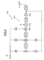
- the device power amplifier DIS has a BE input terminal receiving the signal SG to be amplified, followed by the means of amplification of delta-sigma type MAP power.
- the signal SG comes here from a mixer having transposed the signal SG in the radio frequency domain.
- At least two gains are expected signal (signal amplifiers) arranged between the BE input terminal and the MAP power amplification means.
- signal gains k8-k10 respectively connected between the terminal BE input and adders / subtractors arranged upstream of integration means, formed here by frequency selector networks, INT1-INT2 as well as between the BE input terminal and an adder additional ADD placed between the frequency selector network INT2 and a QTZ quantification means.
- the signal delivered to the output of the ADD adder is then quantized on one bit in the quantization means QTZ.
- the signal, of square wave form, delivered by the means of QTZ quantification is then amplified, after digital conversion analog DAC, in an AMP power amplifier operating here in class E (i.e. on square signals).
- the amplifier output is looped back to the inputs of the adders / subtractors by two continuous gains respectively referenced in this example k1 and k2.
- the output of the AMP amplifier is also connected to the input an FDS post-amplifier filter, which is a bandpass filter, of which the output is connected to the DUP duplexer.
- the means of amplifying MAP power of the delta-sigma type have here, for the sake of simplification of FIG. 2, a global order equal to 2 (since the number of integrators is equal to 2).
- the two frequency selector networks INT1 and INT2 are here capacitive inductive networks respectively tuned on frequencies in the useful signal band, i.e. between 1920 and 1980 MHz in this case.
- the INT1 network can be tuned for example on the frequency of 1940 MHz while the INT2 network can be tuned to the frequency of 1960 MHz.
- the resonance frequencies of different frequency selector networks set the zeros of the noise transfer function, i.e. the frequencies at which eliminates quantization noise.
- the two zeros of the noise transfer function, corresponding to the two resonant frequencies of the networks INT1 and INT2 are intended to meet the requirements of the signal / noise ratio in the useful signal transmission band.
- the poles of the transfer function are fixed by the gains of continuous returns k1 and k2 and are placed so as to stabilize the whole of the system.
- FIG. 2 gives a additional degree of freedom to fix the zeros of the function of signal transfer.
- the zeros and the poles of the noise transfer function are set by the frequencies of the networks frequency selectors as well as by the return gains k1and k2.
- the poles of the signal transfer function are identical at the poles of the noise transfer function.
Landscapes
- Engineering & Computer Science (AREA)
- Theoretical Computer Science (AREA)
- Transmitters (AREA)
- Amplifiers (AREA)
Abstract
Description
- la figure 1 illustre de façon schématique la structure d'un téléphone mobile cellulaire selon l'invention,
- et,
- la figure 2 illustre de façon schématique un mode de réalisation d'un dispositif d'amplification de puissance selon l'invention.
Claims (7)
- Dispositif d'amplification de puissance, comportant une entrée pour recevoir un signal ayant une bande fréquentielle utile, et des moyens d'amplification de puissance du type delta-sigma, caractérisé par le fait que les moyens d'amplification de puissance du type delta-sigma (MAP) présentent un ordre global supérieur ou égal à un, et par le fait que le dispositif comporte au moins deux amplificateurs de signal (k8-k10) connectés entre ladite entrée (BE) et les moyens d'amplification de puissance (MAP), les valeurs relatives de ces gains de signal étant ajustées de façon à localiser les zéros de la fonction de transfert de signal en dehors de ladite bande fréquentielle utile.
- Dispositif selon la revendication 1, caractérisé par le fait qu'il comporte un nombre d'amplificateurs de signal égal à l'ordre global des moyens d'amplification de puissance (MAP), augmenté d'une unité.
- Dispositif selon la revendication 1 ou 2, caractérisé par le fait que les amplificateurs de signal sont à gain programmable.
- Dispositif selon la revendication 1, 2 ou 3, caractérisé par le fait que les moyens d'amplification de puissance (MAP) comportent au moins un réseau sélecteur de fréquence (INT1, INT2) accordé sur une fréquence située dans la bande utile
- Dispositif selon l'une des revendications précédentes, caractérisé par le fait qu'il est réalisé sous la forme d'un circuit intégré.
- Composant d'un système de communication sans fil, caractérisé par le fait qu'il comporte un dispositif d'amplification de puissance selon l'une des revendications 1 à 5.
- Composant selon la revendication 6, caractérisé par le fait qu'il forme un téléphone mobile cellulaire.
Priority Applications (3)
| Application Number | Priority Date | Filing Date | Title |
|---|---|---|---|
| DE60308133T DE60308133T2 (de) | 2003-01-10 | 2003-01-10 | Vorrichtung zur Leistungsverstärkung, insbesondere mit reduzierter Eingangsdynamik, für ein Mobiltelefon |
| EP03290066A EP1437834B1 (fr) | 2003-01-10 | 2003-01-10 | Dispositif d'amplification de puissance, notamment à dynamique d'entrée réduite, en particulier pour un téléphone mobile cellulaire |
| US10/754,464 US7130594B2 (en) | 2003-01-10 | 2004-01-09 | Power amplification device, especially with reduced input dynamic swing, in particular for a cellular mobile telephone |
Applications Claiming Priority (1)
| Application Number | Priority Date | Filing Date | Title |
|---|---|---|---|
| EP03290066A EP1437834B1 (fr) | 2003-01-10 | 2003-01-10 | Dispositif d'amplification de puissance, notamment à dynamique d'entrée réduite, en particulier pour un téléphone mobile cellulaire |
Publications (2)
| Publication Number | Publication Date |
|---|---|
| EP1437834A1 true EP1437834A1 (fr) | 2004-07-14 |
| EP1437834B1 EP1437834B1 (fr) | 2006-09-06 |
Family
ID=32479969
Family Applications (1)
| Application Number | Title | Priority Date | Filing Date |
|---|---|---|---|
| EP03290066A Expired - Lifetime EP1437834B1 (fr) | 2003-01-10 | 2003-01-10 | Dispositif d'amplification de puissance, notamment à dynamique d'entrée réduite, en particulier pour un téléphone mobile cellulaire |
Country Status (3)
| Country | Link |
|---|---|
| US (1) | US7130594B2 (fr) |
| EP (1) | EP1437834B1 (fr) |
| DE (1) | DE60308133T2 (fr) |
Citations (2)
| Publication number | Priority date | Publication date | Assignee | Title |
|---|---|---|---|---|
| US5039989A (en) * | 1989-10-27 | 1991-08-13 | Crystal Semiconductor Corporation | Delta-sigma analog-to-digital converter with chopper stabilization at the sampling frequency |
| WO2001003312A1 (fr) * | 1999-07-06 | 2001-01-11 | Telit Mobile Terminals S.P.A. | Appareil de reception multistandard et procede de definition de parametres associe |
Family Cites Families (4)
| Publication number | Priority date | Publication date | Assignee | Title |
|---|---|---|---|---|
| US5079550A (en) * | 1989-10-27 | 1992-01-07 | Crystal Semiconductor Corporation | Combining continuous time and discrete time signal processing in a delta-sigma modulator |
| US5982315A (en) * | 1997-09-12 | 1999-11-09 | Qualcomm Incorporated | Multi-loop Σ Δ analog to digital converter |
| EP1437827A1 (fr) * | 2003-01-10 | 2004-07-14 | STMicroelectronics N.V. | Dispositif d'amplification de puissance, en particulier pour un téléphone mobile cellulaire |
| US6998910B2 (en) * | 2004-01-22 | 2006-02-14 | Texas Instruments Incorporated | Amplifier using delta-sigma modulation |
-
2003
- 2003-01-10 EP EP03290066A patent/EP1437834B1/fr not_active Expired - Lifetime
- 2003-01-10 DE DE60308133T patent/DE60308133T2/de not_active Expired - Lifetime
-
2004
- 2004-01-09 US US10/754,464 patent/US7130594B2/en not_active Expired - Lifetime
Patent Citations (2)
| Publication number | Priority date | Publication date | Assignee | Title |
|---|---|---|---|---|
| US5039989A (en) * | 1989-10-27 | 1991-08-13 | Crystal Semiconductor Corporation | Delta-sigma analog-to-digital converter with chopper stabilization at the sampling frequency |
| WO2001003312A1 (fr) * | 1999-07-06 | 2001-01-11 | Telit Mobile Terminals S.P.A. | Appareil de reception multistandard et procede de definition de parametres associe |
Also Published As
| Publication number | Publication date |
|---|---|
| DE60308133T2 (de) | 2007-08-09 |
| EP1437834B1 (fr) | 2006-09-06 |
| US20040162045A1 (en) | 2004-08-19 |
| DE60308133D1 (de) | 2006-10-19 |
| US7130594B2 (en) | 2006-10-31 |
Similar Documents
| Publication | Publication Date | Title |
|---|---|---|
| CN1199364C (zh) | 无线电接收器 | |
| EP2359484B1 (fr) | Interface pour dispositifs de radiocommunication | |
| US20120189040A1 (en) | Multi-mode receiver | |
| US20070184804A1 (en) | Method and device for cancelling interferences | |
| EP1835630A1 (fr) | Procédé de minimisation de la fuite de signal dans un système du type à transmission bi-directionnelle simultanée, et dispositif correspondant | |
| FR2926421A1 (fr) | Systeme d'emission radiofrequence | |
| EP2673888A1 (fr) | Terminal bi-bande a acces concurrents operant dans deux bandes adjacentes | |
| EP1306978B1 (fr) | Récepteur à conversion directe pour un système de communication utilisant une modulation à enveloppe non constante | |
| JPH11234150A (ja) | デジタル復調装置 | |
| CN1771666A (zh) | 包括发射机的设备中的信号接收 | |
| EP1248375B1 (fr) | Procédé de conversion analogique/numérique d'un signal analogique au sein d'un terminal d'un système de communication sans fil, par exemple un téléphone mobile, et terminal correspondant. | |
| WO2007101885A1 (fr) | Dispositif de recepion et/ou d'emission de signaux radiofrequences a reduction du bruit | |
| US7593491B1 (en) | Quadrature single-mixer multi-mode radio frequency receiver | |
| Emira et al. | Chameleon: A dual-mode 802.11 b/bluetooth receiver system design | |
| EP0778678B1 (fr) | Récepteur différentiel de signaux à étalement de spectre par séquence directe | |
| EP1437834B1 (fr) | Dispositif d'amplification de puissance, notamment à dynamique d'entrée réduite, en particulier pour un téléphone mobile cellulaire | |
| EP1437827A1 (fr) | Dispositif d'amplification de puissance, en particulier pour un téléphone mobile cellulaire | |
| KR100860629B1 (ko) | 다중 무선 통신 서비스 처리 방법 및 장치 | |
| FR2983016A1 (fr) | Procede de reduction de la consommation de puissance dans un terminal de communication sans fil et terminal de communication mettant en oeuvre ledit procede | |
| EP4082121B1 (fr) | Dispositif radiofréquence | |
| FR2832569A1 (fr) | Procede de transmission de communications dans un systeme de telecommunication de type cellulaire utilisant des bandes de frequences porteuses adjacentes | |
| EP1564883A1 (fr) | Procédé et dispositif de transposition de fréquence, en particulier pour le contrôle de la puissance d'émission d'un téléphone mobile cellulaire | |
| FR2926422A1 (fr) | Systeme d'emission radiofrequence | |
| FR3079376A1 (fr) | Module de génération d’options de réception de signaux radio | |
| FR2896370A1 (fr) | Dispositif et methode d'amelioration du rapport porteuse a bruit pour un recepteur a diversite |
Legal Events
| Date | Code | Title | Description |
|---|---|---|---|
| PUAI | Public reference made under article 153(3) epc to a published international application that has entered the european phase |
Free format text: ORIGINAL CODE: 0009012 |
|
| AK | Designated contracting states |
Kind code of ref document: A1 Designated state(s): AT BE BG CH CY CZ DE DK EE ES FI FR GB GR HU IE IT LI LU MC NL PT SE SI SK TR |
|
| AX | Request for extension of the european patent |
Extension state: AL LT LV MK RO |
|
| 17P | Request for examination filed |
Effective date: 20041217 |
|
| AKX | Designation fees paid |
Designated state(s): DE FR GB IT |
|
| GRAP | Despatch of communication of intention to grant a patent |
Free format text: ORIGINAL CODE: EPIDOSNIGR1 |
|
| GRAS | Grant fee paid |
Free format text: ORIGINAL CODE: EPIDOSNIGR3 |
|
| GRAA | (expected) grant |
Free format text: ORIGINAL CODE: 0009210 |
|
| AK | Designated contracting states |
Kind code of ref document: B1 Designated state(s): DE FR GB IT |
|
| PG25 | Lapsed in a contracting state [announced via postgrant information from national office to epo] |
Ref country code: IT Free format text: LAPSE BECAUSE OF FAILURE TO SUBMIT A TRANSLATION OF THE DESCRIPTION OR TO PAY THE FEE WITHIN THE PRESCRIBED TIME-LIMIT;WARNING: LAPSES OF ITALIAN PATENTS WITH EFFECTIVE DATE BEFORE 2007 MAY HAVE OCCURRED AT ANY TIME BEFORE 2007. THE CORRECT EFFECTIVE DATE MAY BE DIFFERENT FROM THE ONE RECORDED. Effective date: 20060906 |
|
| REG | Reference to a national code |
Ref country code: GB Ref legal event code: FG4D Free format text: NOT ENGLISH |
|
| REF | Corresponds to: |
Ref document number: 60308133 Country of ref document: DE Date of ref document: 20061019 Kind code of ref document: P |
|
| GBT | Gb: translation of ep patent filed (gb section 77(6)(a)/1977) |
Effective date: 20060929 |
|
| PLBE | No opposition filed within time limit |
Free format text: ORIGINAL CODE: 0009261 |
|
| STAA | Information on the status of an ep patent application or granted ep patent |
Free format text: STATUS: NO OPPOSITION FILED WITHIN TIME LIMIT |
|
| 26N | No opposition filed |
Effective date: 20070607 |
|
| REG | Reference to a national code |
Ref country code: FR Ref legal event code: PLFP Year of fee payment: 14 |
|
| REG | Reference to a national code |
Ref country code: DE Ref legal event code: R081 Ref document number: 60308133 Country of ref document: DE Owner name: FRANCE BREVETS, FR Free format text: FORMER OWNERS: STMICROELECTRONICS N.V., AMSTERDAM, NL; STMICROELECTRONICS S.R.L., AGRATE BRIANZA, IT Ref country code: DE Ref legal event code: R082 Ref document number: 60308133 Country of ref document: DE Representative=s name: VOSSIUS & PARTNER PATENTANWAELTE RECHTSANWAELT, DE Ref country code: DE Ref legal event code: R081 Ref document number: 60308133 Country of ref document: DE Owner name: STMICROELECTRONICS INTERNATIONAL N.V., NL Free format text: FORMER OWNERS: STMICROELECTRONICS N.V., AMSTERDAM, NL; STMICROELECTRONICS S.R.L., AGRATE BRIANZA, IT |
|
| REG | Reference to a national code |
Ref country code: GB Ref legal event code: 732E Free format text: REGISTERED BETWEEN 20161013 AND 20161019 |
|
| REG | Reference to a national code |
Ref country code: FR Ref legal event code: TQ Owner name: STMICROELECTRONICS INTERNATIONAL N.V., NL Effective date: 20161011 Ref country code: FR Ref legal event code: TP Owner name: STMICROELECTRONICS INTERNATIONAL N.V., NL Effective date: 20161011 |
|
| REG | Reference to a national code |
Ref country code: FR Ref legal event code: PLFP Year of fee payment: 15 |
|
| REG | Reference to a national code |
Ref country code: DE Ref legal event code: R082 Ref document number: 60308133 Country of ref document: DE Representative=s name: VOSSIUS & PARTNER PATENTANWAELTE RECHTSANWAELT, DE Ref country code: DE Ref legal event code: R081 Ref document number: 60308133 Country of ref document: DE Owner name: FRANCE BREVETS, FR Free format text: FORMER OWNER: STMICROELECTRONICS INTERNATIONAL N.V., SCHIPHOL, NL |
|
| REG | Reference to a national code |
Ref country code: FR Ref legal event code: PLFP Year of fee payment: 16 |
|
| PGFP | Annual fee paid to national office [announced via postgrant information from national office to epo] |
Ref country code: FR Payment date: 20211224 Year of fee payment: 20 Ref country code: GB Payment date: 20211216 Year of fee payment: 20 |
|
| PGFP | Annual fee paid to national office [announced via postgrant information from national office to epo] |
Ref country code: DE Payment date: 20211222 Year of fee payment: 20 |
|
| PGFP | Annual fee paid to national office [announced via postgrant information from national office to epo] |
Ref country code: IT Payment date: 20211230 Year of fee payment: 20 |
|
| REG | Reference to a national code |
Ref country code: DE Ref legal event code: R071 Ref document number: 60308133 Country of ref document: DE |
|
| REG | Reference to a national code |
Ref country code: GB Ref legal event code: PE20 Expiry date: 20230109 |
|
| PG25 | Lapsed in a contracting state [announced via postgrant information from national office to epo] |
Ref country code: GB Free format text: LAPSE BECAUSE OF EXPIRATION OF PROTECTION Effective date: 20230109 |