EP1437763A1 - Semiconductor manufacturing apparatus and method for manufacturing semiconductor device - Google Patents
Semiconductor manufacturing apparatus and method for manufacturing semiconductor device Download PDFInfo
- Publication number
- EP1437763A1 EP1437763A1 EP02779906A EP02779906A EP1437763A1 EP 1437763 A1 EP1437763 A1 EP 1437763A1 EP 02779906 A EP02779906 A EP 02779906A EP 02779906 A EP02779906 A EP 02779906A EP 1437763 A1 EP1437763 A1 EP 1437763A1
- Authority
- EP
- European Patent Office
- Prior art keywords
- main body
- controller unit
- processing apparatus
- apparatus main
- internal information
- Prior art date
- Legal status (The legal status is an assumption and is not a legal conclusion. Google has not performed a legal analysis and makes no representation as to the accuracy of the status listed.)
- Withdrawn
Links
Images


Classifications
-
- H—ELECTRICITY
- H10—SEMICONDUCTOR DEVICES; ELECTRIC SOLID-STATE DEVICES NOT OTHERWISE PROVIDED FOR
- H10P—GENERIC PROCESSES OR APPARATUS FOR THE MANUFACTURE OR TREATMENT OF DEVICES COVERED BY CLASS H10
- H10P95/00—Generic processes or apparatus for manufacture or treatments not covered by the other groups of this subclass
-
- H—ELECTRICITY
- H10—SEMICONDUCTOR DEVICES; ELECTRIC SOLID-STATE DEVICES NOT OTHERWISE PROVIDED FOR
- H10P—GENERIC PROCESSES OR APPARATUS FOR THE MANUFACTURE OR TREATMENT OF DEVICES COVERED BY CLASS H10
- H10P72/00—Handling or holding of wafers, substrates or devices during manufacture or treatment thereof
- H10P72/06—Apparatus for monitoring, sorting, marking, testing or measuring
- H10P72/0612—Production flow monitoring, e.g. for increasing throughput
-
- C—CHEMISTRY; METALLURGY
- C23—COATING METALLIC MATERIAL; COATING MATERIAL WITH METALLIC MATERIAL; CHEMICAL SURFACE TREATMENT; DIFFUSION TREATMENT OF METALLIC MATERIAL; COATING BY VACUUM EVAPORATION, BY SPUTTERING, BY ION IMPLANTATION OR BY CHEMICAL VAPOUR DEPOSITION, IN GENERAL; INHIBITING CORROSION OF METALLIC MATERIAL OR INCRUSTATION IN GENERAL
- C23C—COATING METALLIC MATERIAL; COATING MATERIAL WITH METALLIC MATERIAL; SURFACE TREATMENT OF METALLIC MATERIAL BY DIFFUSION INTO THE SURFACE, BY CHEMICAL CONVERSION OR SUBSTITUTION; COATING BY VACUUM EVAPORATION, BY SPUTTERING, BY ION IMPLANTATION OR BY CHEMICAL VAPOUR DEPOSITION, IN GENERAL
- C23C16/00—Chemical coating by decomposition of gaseous compounds, without leaving reaction products of surface material in the coating, i.e. chemical vapour deposition [CVD] processes
- C23C16/44—Chemical coating by decomposition of gaseous compounds, without leaving reaction products of surface material in the coating, i.e. chemical vapour deposition [CVD] processes characterised by the method of coating
- C23C16/52—Controlling or regulating the coating process
-
- C—CHEMISTRY; METALLURGY
- C23—COATING METALLIC MATERIAL; COATING MATERIAL WITH METALLIC MATERIAL; CHEMICAL SURFACE TREATMENT; DIFFUSION TREATMENT OF METALLIC MATERIAL; COATING BY VACUUM EVAPORATION, BY SPUTTERING, BY ION IMPLANTATION OR BY CHEMICAL VAPOUR DEPOSITION, IN GENERAL; INHIBITING CORROSION OF METALLIC MATERIAL OR INCRUSTATION IN GENERAL
- C23C—COATING METALLIC MATERIAL; COATING MATERIAL WITH METALLIC MATERIAL; SURFACE TREATMENT OF METALLIC MATERIAL BY DIFFUSION INTO THE SURFACE, BY CHEMICAL CONVERSION OR SUBSTITUTION; COATING BY VACUUM EVAPORATION, BY SPUTTERING, BY ION IMPLANTATION OR BY CHEMICAL VAPOUR DEPOSITION, IN GENERAL
- C23C16/00—Chemical coating by decomposition of gaseous compounds, without leaving reaction products of surface material in the coating, i.e. chemical vapour deposition [CVD] processes
- C23C16/44—Chemical coating by decomposition of gaseous compounds, without leaving reaction products of surface material in the coating, i.e. chemical vapour deposition [CVD] processes characterised by the method of coating
- C23C16/54—Apparatus specially adapted for continuous coating
Definitions
- the present invention relates to a semiconductor manufacturing technique and, more particularly, to a semiconductor manufacturing apparatus which executes a plurality of processes such as an oxidation, a diffusion, and CVD (a Chemical Vapor Deposition) in a single chamber and a semiconductor device manufacturing method using the semiconductor manufacturing apparatus.
- a semiconductor manufacturing apparatus which executes a plurality of processes such as an oxidation, a diffusion, and CVD (a Chemical Vapor Deposition) in a single chamber and a semiconductor device manufacturing method using the semiconductor manufacturing apparatus.
- FIG. 7 is a flow chart showing the continuous process flow of the film formation process of an oxide film and SiN film based on a prior art.
- the oxide film formation temperature, the oxidation gas flow rate, the oxidation time, the SiN deposition temperature, the SiN deposition time, the gas pressure in SiN film formation, the SiN film formation gas flow rate, and the like are input to the control computer of a semiconductor manufacturing apparatus (in this case, an oxidation/CVD furnace) by some means such that desired film thicknesses can be obtained, respectively.
- a start signal is input by some means to start the process.
- Processes such as a wafer loading into the apparatus, a heating up, a temperature retention, gas supplies, gas switchings, a cooling down, and a wafer unloading are performed in accordance with the set sequence.
- the temperature in the furnace and the gas flow rate are kept at the set values as exactly as possible, and the oxidation time and deposition time are controlled, thereby obtaining the desired film thicknesses.
- a fluctuation in film thickness or a fluctuation in impurity dose due to uncontrollable disturbance factors in the apparatus or a fluctuation in film thickness or a fluctuation in impurity dose due to uncontrollable disturbance factors outside of the apparatus are not taken into consideration at all.
- uncontrollable disturbance factors in the apparatus are a slight change in temperature in heating due to the influence of the process temperature for the preceding batch and a very small change in gas flow rate due to a slight variation in supply voltage.
- An example of uncontrollable disturbance factors outside the apparatus is a change in the atmospheric pressure.
- Jpn. Pat. Appln. KOKAI Publication Nos. 11-288856 and 8-55145 describe ideas for comparing actual manufacturing data with simulated data.
- the purpose of comparison in these prior arts is to improve the accuracy of simulation or adjust simulated data to actual manufacturing data, which is anything but a proposal from the viewpoint of manufacturing control in changing manufacturing conditions or manufacturing parameters.
- no calculation is performed presuming disturbances inside and outside of the apparatus, so a variation in manufacturing each cycle is not taken into consideration.
- the present invention employs the following arrangements.
- a semiconductor manufacturing apparatus comprising a processing apparatus main body which continuously executes a plurality of processes related to manufacturing of a semiconductor device in a single chamber, and an apparatus controller unit which selects a type of process to be carried out in the processing apparatus main body and supplies a start signal to start a process and a stop signal to stop the process to the processing apparatus main body, characterized by comprising a first terminal to output internal information of the processing apparatus main body to an outside, a second terminal to output the start signal from the apparatus controller unit to the outside, and a third terminal to receive the start signal from the second terminal and input to the apparatus controller unit the stop signal based on a result obtained by calculating the process state for the current process on the basis of the internal information of the apparatus, wherein the apparatus controller unit sends the stop signal to the processing apparatus main body upon receiving the stop signal from the third terminal, stops the current process by the processing apparatus main body, and switches to the next process.
- a semiconductor manufacturing apparatus characterized by comprising a processing apparatus main body which continuously executes a plurality of processes related to manufacturing of a semiconductor device in a single chamber, an apparatus controller unit which selects a type of process to be carried out in the processing apparatus main body and supplies a start signal to start a process and a stop signal to stop the process to the processing apparatus main body, and a process controller unit which has a function of calculating process states for the plurality of processes on the basis of internal information of the processing apparatus main body, starts calculating the process state for the current process at a timing when the start signal is sent from the apparatus controller unit, and sends the stop signal to the apparatus controller unit when the process state reaches to a specified state, wherein the apparatus controller unit sends the stop signal to the processing apparatus main body upon receiving the stop signal from the process controller unit, stops the current process by the processing apparatus main body, and switches to the next process.
- a semiconductor device manufacturing method of executing a predetermined process for a substrate to be processed using a semiconductor manufacturing apparatus comprising a processing apparatus main body which continuously executes a plurality of processes related to manufacturing of a semiconductor device in a single chamber, an apparatus controller unit which selects a type of process to be carried out in the processing apparatus main body and controls a start and a stop of the process, and a process controller unit which has a function of calculating process states for the plurality of processes on the basis of internal information of the processing apparatus main body, characterized by comprising while the substrate to be processed is set in the processing apparatus main body, causing the apparatus controller unit to start the predetermined process, causing the process controller unit to start calculating a process state for the current process, and when it is judged on the basis of a calculation result that the process state reaches a specified state, causing the apparatus controller unit to stop the current process and switch to the next process.
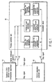
- FIG. 1 is a block diagram showing the basic arrangement of a semiconductor manufacturing apparatus according to the first embodiment of the present invention. Note that the semiconductor manufacturing apparatus of this embodiment can be applied to either a batch processing apparatus or a single wafer processing apparatus.
- a chamber 10 continuously executes a plurality of processes and is constituted by, e.g., an oxidation/diffusion/CVD furnace (to be referred to as a multiprocess apparatus hereinafter).
- An internal apparatus controller (apparatus controller unit) 20 controls the multiprocess apparatus 10.
- a process controller unit 30 has a film thickness calculation function, a doping amount calculation function, a calculated film thickness judgment function, a calculated doping amount judgment function, and the like.
- the internal apparatus controller 20 has an external output signal generator 21 having a process time monitoring function, a process data storage function, and the like. Upon receiving a calculation result and a stop signal from the process controller unit 30, the external output signal generator 21 outputs a stop signal to the multiprocess apparatus 10. In addition, upon receiving a process start signal by user input, or a predetermined time after the output of the stop signal, the external output signal generator 21 sends a start signal to the multiprocess apparatus 10.
- reference numeral 41 denotes a first terminal which sends internal information of the apparatus to the outside; 42, a second terminal which sends a start signal to the outside; and 43, a third terminal which receives a stop signal from the outside.
- the multiprocess apparatus 10 operates under the control of the internal apparatus controller 20.
- a start signal is sent from the internal apparatus controller 20 in the multiprocess apparatus 10 to the multiprocess apparatus 10 and process controller unit 30 at a timing in a predetermined process sequence.
- the process controller unit 30 judges on the basis of information such as a process gas in the apparatus which one, a deposited film thickness, an oxide film thickness, or a doping amount, should be calculated. Then, the process controller unit 30 actually starts calculating one of the deposited film thickness, the oxide film thickness, or the doping amount.
- the internal apparatus controller 20 Under the control of the internal apparatus controller 20 according to the set sequence, a wafer loading into the multiprocess apparatus 10, a heating up, and a temperature retention are performed. Next, the internal apparatus controller 20 instructs the multiprocess apparatus 10 to supply a process gas and simultaneously sends a start signal to the process controller unit 30.
- the starting point is set at the time of start of process gas supply. However, the starting point can be changed in advance in accordance with the purpose by presetting the timing, e.g., to a time after wafer loading into the multiprocess apparatus 10 is finished, before a heating up is started, or when the temperature of inside of the wafer furnace reaches to a predetermined temperature.
- the oxide film thickness is calculated first.
- Internal information of the apparatus is used for the calculation.
- temperature information from various thermocouples inside or outside of the furnace, a gas flow rate from a flowmeter, and the like can be used.
- tox is the oxide film thickness
- ⁇ is the initial film thickness
- t is the time
- B/A is the primary coefficient
- B is the secondary coefficient.
- ⁇ uses a value of 15 nm
- B/A uses a value of 5 ⁇ 10 -6
- B uses a value of 8 ⁇ 10 -6 min/ ⁇ m.
- the temperature and the gas flow rate which change every moment, are read at a predetermined time interval of, e.g., 1 sec.
- a predetermined time interval of, e.g., 1 sec.
- an increment of the oxide film thickness during the time interval is calculated and a total oxide film thickness at that time can be calculated by accumulating increments. Accordingly, a fluctuation in oxide film thickness due to disturbances such as changes in the temperature and the flow rate can be taken into consideration. Such disturbances cannot be taken into consideration in the conventional oxidation method.
- the time interval is set to 1 sec because if the oxide film thickness should be controlled within ⁇ 0.2 nm, the apparatus must be controlled within an accuracy of ⁇ 2 sec, then the sampling rate must be less than ⁇ 2 sec.
- the calculation result of the oxide film thickness is judged by the calculated film thickness judgment function.
- a stop signal is sent from the process controller unit 30 to the internal apparatus controller 20.
- the internal apparatus controller 20 sends the stop signal to the multiprocess apparatus 10 to stop oxidation.
- this control corresponds to sending from internal apparatus controller 20 to the multiprocess apparatus 10, e.g., an interrupt instruction "to end the sequence for supplying the oxidation gas and switch to a sequence for supplying the next inert gas".
- This timing may be set a little before the it comes. That is, if there is a case that the oxidation gas cannot immediately be switched to the next gas after the output of the stop signal until the end of oxidation, extra oxidation is performed. Expecting this extra oxidation, a slightly smaller value than the target film thickness is to be set as a judgment film thickness.
- the multiprocess apparatus 10 When an SiN film is to be deposited continuously after formation of the oxide film, the multiprocess apparatus 10 receives the stop signal after the end of oxide film formation and then receives a start signal again from the internal apparatus controller 20.
- the process controller unit 30 receives the start signal again and judges on the basis of the internal information of the apparatus, such as the process gas, which one, the oxide film thickness, the deposited film thickness, or the doping amount, should be calculated.
- SiN film formation is performed next.
- the sequence advances to calculation of the deposited film thickness.
- Internal information of the apparatus is used for calculation.
- temperature information from various thermocouples inside and outside of the furnace, a gas flow rate from a flowmeter, a process pressure from a pressure gauge, and the like can be used.
- the temperature, the gas flow rate, and the process pressure, which change every moment, are read at a predetermined time interval of, e.g., 1 sec.
- an increment of the deposited film thickness during the time interval is calculated and a total deposited film thickness at that time can be calculated by accumulating increments. Accordingly, a fluctuation in deposited film thickness due to disturbances such as changes in the temperature, the flow rate, and the pressure can be taken into consideration. Such disturbances cannot be taken into consideration in the conventional deposited film thickness control.
- the calculation result of the deposited film thickness is judges by the calculated film thickness judgment function.
- a stop signal is sent from the process controller unit 30 to the internal apparatus controller 20.
- the internal apparatus controller 20 sends the stop signal to the multiprocess apparatus 10 to stop deposition of the SiN film.
- this control corresponds to sending from the internal apparatus controller 20 to the multiprocess apparatus 10, e.g., an interrupt instruction "to end the sequence for supplying the deposition gas and switch to a sequence for supplying the next inert gas".
- This timing may be set a little before it comes. That is, if there is a case that the deposition gas cannot immediately be switched to the next gas after the output of the stop signal until the end of deposition, an extra deposition is performed. Expecting this extra deposition, a slightly smaller value than the target film thickness is to be set as a judgment film thickness.
- a cooling down and a wafer unloading instructions are output from the internal apparatus controller 20 in accordance with a predetermined sequence.
- the multiprocess apparatus 10 executes these processes, and the process is ended.
- the variations in film thickness among wafers due to the continuous process occur due to fluctuations in temperature in the furnace, the gas flow rate, the process pressure, and the like, which are uncontrollable before.
- film thickness calculation is performed in consideration of these fluctuations, and the result is fed back to the process, strict film thickness control with little variation can be performed.
- the process controller unit 30 by causing the process controller unit 30 to calculate the quality characteristic in real time on the basis of the internal information of the apparatus and control the process time, very strict control against disturbances can be executed. More specifically, the function of receiving in real time internal information of the apparatus, including the temperature inside of the furnace, the pressure inside of the furnace, and the gas flow rate, and information outside the apparatus such as the atmospheric pressure, the function of converting the received information for values available for calculation, the function of calculating the oxide film thickness, deposited film thickness, impurity diffusion length, and the like in real time, the function of selecting an algorithm (oxidation/deposition/diffusion) for real time calculation, and the function of starting calculation in accordance with a process start signal of the apparatus and outputting a process end signal to the apparatus when a desired film thickness or doping amount is obtained.
- the function of receiving in real time internal information of the apparatus including the temperature inside of the furnace, the pressure inside of the furnace, and the gas flow rate, and information outside the apparatus such as the atmospheric pressure
- the process time can strictly be controlled. Hence, any fluctuation in film thickness due to uncontrollable disturbance factors in the apparatus or any fluctuation in film thickness due to uncontrollable disturbance factors such as the atmospheric pressure outside of the apparatus can be suppressed, and sufficient element device performance and circuit characteristics can be obtained.
- FIG. 3 is an arithmetic flow chart in the process controller section 30 according to this embodiment. A method of performing oxide film calculation and deposited film thickness calculation will be described with reference to FIG. 3.
- step S1 film thickness calculation and doping amount calculation are initialized (step S1).
- step S2 the start signal from the internal apparatus controller 20 is monitored (step S2).
- step S3 the internal information of the apparatus is received (step S3). It is judged which one, the oxide film thickness calculation or the deposited film thickness calculation should be performed (step S4).
- oxide film thickness calculation is performed first (step S12). It is judged whether the calculated oxide film thickness exceeds the specified value, and in this case, 60 nm (step S13). If NO in step S13, the process waits for another 1 sec from the preceding internal information acquisition, and then, the internal information is acquired again (step S11), and oxide film thickness calculation is performed in step S12 again. This process is repeated. When the calculated oxide film thickness exceeds 60 nm, a stop signal is sent to the internal apparatus controller 20 (step S5). It is judged whether all processes are ended (step S6). If another process remains, the flow returns to the start.
- step S1 After the oxide film thickness calculation, a film thickness calculation and a doping amount calculation are initialized in step S1.
- step S2 the start signal is monitored. When the start signal is output, the internal information of the apparatus is received in step S3. It is judged in step S4 which one, the oxide film thickness calculation or the deposited film thickness calculation, should be performed.
- step S22 a SiN deposited film thickness is calculated (step S22). It is judged whether the calculated deposited film thickness exceeds the specified value, and in this case, 100 nm (step S23). If NO in step S23, the process waits for another 1 sec from the preceding internal information acquisition, and then, the internal information is acquired again (step S21), and deposited film thickness calculation is performed in step S22. This process is repeated. When the calculated deposited film thickness exceeds 100 nm, a stop signal is sent to the internal apparatus controller 20 in step S5. If it is judged in step S6 that all processes are ended, the process is ended.
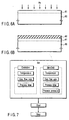
- FIG. 4A is a sectional (view) showing a state wherein an SiO 2 film 51 is formed on an Si substrate 50 in the multiprocess apparatus 10 by steps S2 to S5 of the first cycle.
- FIG. 4B is a sectional (view) showing a state wherein an SiN film 52 is formed on the SiO 2 film 51 in the multiprocess apparatus 10 by steps S2 to S5 of the second cycle. Both film thicknesses could be accurately controlled.
- the process controller unit 30 is arranged to monitor in real time the oxidation process and deposition process in the multiprocess apparatus 10 and control the process time. Accordingly, the process variation for each wafer in the continuous processing can be reduced. In addition, the accuracy of calculation for the plurality of processes can be improved. For an oxide film thickness, 0.1-nm order film thickness control can be performed. Furthermore, since the gate oxide film and a poly-Si silicon film for an electrode can be continuously formed, the yield and reliability of devices can greatly be increased.
- the continuous formation process of oxide film formation and SiN film deposition has been exemplified.
- an example of a continuous process of As vapor phase diffusion and a thermal oxidation will be described.
- the apparatus arrangement of the semiconductor manufacturing apparatus is the same as in FIG. 1.
- a doping amount calculation is performed first.
- Internal information of the apparatus is used for calculation.
- temperature information from various thermocouples inside and outside of the furnace, a gas flow rate from a flowmeter, a process pressure from a pressure gauge, and the like can be used.
- the temperature, the gas flow rate, and the process pressure, which change every moment, are read at a predetermined time interval of, e.g., 1 sec.
- a predetermined time interval e.g. 1 sec.
- an increment in doping amount during a time interval is calculated and a total doping amount at that time can be calculated by accumulating increments. Accordingly, a fluctuation in doping amount due to disturbances such as changes in the temperature or the flow rate can be taken into consideration. Such disturbances cannot be taken into consideration in the conventional vapor phase diffusion method.
- the calculation result of the doping amount is judged by the calculated doping amount judgment function.
- a stop signal is sent from a process controller unit 30 to an internal apparatus controller 20.
- the internal apparatus controller 20 sends the stop signal to a multiprocess apparatus 10 to stop the vapor phase diffusion process.
- this control corresponds to sending an interrupt instruction from the internal apparatus controller 20 to the multiprocess apparatus 10, e.g., the interrupt instruction is "to end the sequence for supplying the doping gas and switch to a sequence for supplying the next inert gas".
- This timing may be set a little before it comes. That is, if there is a case that the doping gas cannot immediately be switched to a next inert gas after the output of the stop signal until the end of vapor phase diffusion, extra vapor phase diffusion is performed. Expecting this extra vapor phase diffusion, a slightly smaller value than the target doping amount is to be set as a judgment doping amount.
- the process controller unit 30 receives the stop signal after the end of vapor phase diffusion and then receives a start signal again from the internal apparatus controller 20.
- the process controller unit 30 receives the signal and judges on the basis of the internal information of the apparatus, such as the process gas, which one, the oxide film thickness, the deposited film thickness, or the doping amount, should be calculated.
- oxide film formation is performed next.
- the sequence advances to the oxide film thickness calculation algorithm.
- Internal information of the apparatus is used for calculation, as in the first embodiment.
- equation (1) can be used.
- the temperature and gas flow rate which change every moment, are read at a predetermined time interval of, e.g., 1 sec.
- a predetermined time interval of, e.g., 1 sec.
- an increment of the oxide film thickness during a time interval is calculated and total oxide film thickness at that time is calculated by accumulating increments. Accordingly, a fluctuation in the oxide film thickness due to disturbances such as changes in the temperature and the flow rate can be taken into consideration. Such disturbances cannot be taken into consideration in the conventional oxidation method.
- the time interval is set to 1 sec because if the oxide film thickness should be controlled within ⁇ 0.2 nm, the apparatus must be controlled within an accuracy of ⁇ 2 sec, and the sampling rate must be less than ⁇ 2 sec.
- the calculation result of the oxide film thickness is judged by the calculated film thickness judgment function.
- a stop signal is sent from the process controller unit 30 to the internal apparatus controller 20.
- the internal apparatus controller 20 sends the stop signal to the multiprocess apparatus 10 to stop the oxidation.
- this control corresponds to sending an interrupt instruction from internal apparatus controller 20 to the oxidation furnace, e.g., an interrupt instruction is "to end the sequence for supplying the oxidation gas and switch to a sequence for supplying the next inert gas".
- This timing may be set a little before it comes. That is, if there is a case that the oxidation gas cannot immediately be switched to the next gas after the output of the stop signal until the end of oxidation, extra oxidation is performed. Expecting this extra oxidation, a slightly smaller value than the target film thickness is set as a judgment film thickness.
- the fluctuation in film thickness and doping amount among wafers in the continuous process occur due to small changes in the temperature in the furnace, the gas flow rate, the process pressure, and the like, which are uncontrollable before.
- the apparatus and control method of this embodiment when film thickness calculation is performed in consideration of these variations, and the result is fed back to the process, strict film thickness control with little variation can be performed.
- FIG. 5 is an arithmetic flow chart in the process controller unit 30 according to this embodiment. A method of performing deposited film thickness calculation and doping amount calculation will be described with reference to FIG. 5.
- step S1 film thickness calculation and doping amount calculation are initialized (step S1).
- step S2 the start signal from the internal apparatus controller 20 is monitored (step S2).
- step S3 the internal information of the apparatus is received (step S3). It is judged which one, oxide film thickness calculation or doping amount calculation, should be performed (step S4).
- step S32 doping amount calculation is performed first (step S32). It is judged whether the calculated doping amount exceeds the specified value, and in this case, 1 ⁇ 10 20 atoms/cm 2 (step S33). If NO in step S33, the process waits for another 1 sec from the preceding internal information acquisition, and then, the internal information is acquired again (step S31), and doping amount calculation is performed in step S32. This process is repeated. When the calculated doping amount exceeds 1 ⁇ 10 20 atoms/cm 2 , a stop signal is sent to the internal apparatus controller 20 (step S5), and the flow returns to the start.
- step S2 the film thickness calculation and the doping amount calculation are initialized in step S1.
- step S2 the start signal is monitored. When the start signal is output, the internal information of the apparatus is received in step S3. It is judged in step S4 which one, oxide film thickness calculation, doping amount calculation, or deposited film thickness calculation, should be performed. This time, oxide film thickness is calculated (step S12). It is judged whether the calculated oxide film thickness exceeds the specified value, and in this case, 60 nm (step S13). If NO in step S13, the process waits for another 1 sec from the preceding internal information acquisition, and then, the internal information is acquired again (step S11), and oxide film thickness calculation is performed in step S12. This process is repeated. When the calculated oxide film thickness exceeds 60 nm, a stop signal is sent to the internal apparatus controller 20 (step S5). If it is judged in step S6 that all processes are ended, the process is ended.
- the arithmetic flow chart in the process controller unit 30 according to this embodiment has been described above.
- the flow chart is different from the first embodiment only in the types and order of processes.
- FIG. 6A is a sectional view showing a state wherein an As diffusion layer 61 is formed on an Si substrate 60 in the multiprocess apparatus 10 by steps S2 to S5 of the first cycle.
- FIG. 6B is a sectional view showing a state wherein an SiO 2 film 62 is formed on the Si substrate 60 in the multiprocess apparatus 10 by steps S2 to S5 of the second cycle. Both the depth of the diffusion layer 61 and the film thickness of the SiO 2 film 62 could be accurately controlled.
- the process controller unit 30 is arranged to monitor in real time the diffusion process and the oxidation process in the multiprocess apparatus 10 and controls the process time. Hence, the same effect as in the above-described first embodiment can be obtained, as a matter of course. In addition, even when the process state is difficult to calculate, like an ion implantation without reaction, accurate calculation can be performed.
- the dedicated process controller unit is arranged for the multiprocess apparatus.
- the function of the process controller unit may be implemented by an external computer.
- the process controller unit performs calculation on the basis of internal information of the apparatus.
- the calculation may be done on the basis of external information such as the atmospheric pressure as well as the internal information of the apparatus.
- the processes are not limited to oxidation/diffusion/CVD.
- the present invention can be applied to various processes used to manufacture a semiconductor device.
- the process state for the current process is started at a timing when a start signal from the apparatus controller unit is sent, and a stop signal is sent to the apparatus controller unit when the process state reaches to a specified state, thereby suppressing any fluctuation in film thickness due to uncontrollable disturbance factors in the apparatus or any fluctuation in film thickness due to uncontrollable disturbance factors such as the atmospheric pressure outside the apparatus.
- a start signal from the apparatus controller unit is sent
- a stop signal is sent to the apparatus controller unit when the process state reaches to a specified state
Landscapes
- Chemical & Material Sciences (AREA)
- General Chemical & Material Sciences (AREA)
- Chemical Kinetics & Catalysis (AREA)
- Engineering & Computer Science (AREA)
- Materials Engineering (AREA)
- Mechanical Engineering (AREA)
- Metallurgy (AREA)
- Organic Chemistry (AREA)
- Chemical Vapour Deposition (AREA)
Abstract
A semiconductor manufacturing apparatus which
continuously executes oxidation and CVD in a
multiprocess apparatus (10) includes an internal
apparatus controller (20) which selects the type of
process and supplies a start signal and stop signal for
the process to the multiprocess apparatus (10), and
a process controller (30) which calculates the process
state for each process on the basis of the internal
information of the apparatus. Upon receiving the stop
signal from the controller (30), the controller (20)
sends the stop signal to the multiprocess apparatus
(10) to stop the current process by the multiprocess
apparatus (10) and switches to the next process.
Description
The present invention relates to a semiconductor
manufacturing technique and, more particularly, to
a semiconductor manufacturing apparatus which executes
a plurality of processes such as an oxidation,
a diffusion, and CVD (a Chemical Vapor Deposition) in a
single chamber and a semiconductor device manufacturing
method using the semiconductor manufacturing apparatus.
In recent years, a technique for continuously
executing a plurality of processes in a single chamber
has been developed aiming at shortening the wafer
process time in a semiconductor manufacturing
apparatus. In such an apparatus, accurate control
related to a film thickness and an impurity diffusion
is required for the plurality of processes in the
single chamber.
FIG. 7 is a flow chart showing the continuous
process flow of the film formation process of an oxide
film and SiN film based on a prior art. First, on
the basis of technical experiences, the oxide film
formation temperature, the oxidation gas flow rate,
the oxidation time, the SiN deposition temperature,
the SiN deposition time, the gas pressure in SiN film
formation, the SiN film formation gas flow rate,
and the like are input to the control computer of
a semiconductor manufacturing apparatus (in this case,
an oxidation/CVD furnace) by some means such that
desired film thicknesses can be obtained, respectively.
Next, a start signal is input by some means to start
the process.
Processes such as a wafer loading into the
apparatus, a heating up, a temperature retention, gas
supplies, gas switchings, a cooling down, and a wafer
unloading are performed in accordance with the set
sequence. During the processes, the temperature in
the furnace and the gas flow rate are kept at the set
values as exactly as possible, and the oxidation time
and deposition time are controlled, thereby obtaining
the desired film thicknesses.
In the above sequence, however, a fluctuation in
film thickness or a fluctuation in impurity dose due to
uncontrollable disturbance factors in the apparatus or
a fluctuation in film thickness or a fluctuation
in impurity dose due to uncontrollable disturbance
factors outside of the apparatus are not taken into
consideration at all. Examples of uncontrollable
disturbance factors in the apparatus are a slight
change in temperature in heating due to the influence
of the process temperature for the preceding batch
and a very small change in gas flow rate due to
a slight variation in supply voltage. An example of
uncontrollable disturbance factors outside the
apparatus is a change in the atmospheric pressure.
Since a feature size of devices is becoming finer,
and these disturbance factors cannot be neglected
nowadays, no sufficient element device performance
and circuit characteristics can be obtained with
the conventional film formation technique. For this
reason, a semiconductor manufacturing apparatus control
method that takes these disturbance factors into
consideration has been demanded. In addition, since
film thickness measurement, which is performed after
the process, is not performed after the first film
formation in the continuous process, more accurate film
formation control is required.
To examine the influence of the above disturbance
factors on the film thickness or impurity diffusion,
calculation or simulation for an oxidation, a
deposition, and an impurity diffusion is necessary.
For example, Jpn. Pat. Appln. KOKAI Publication
Nos. 11-288856 and 8-55145 describe ideas for comparing
actual manufacturing data with simulated data.
However, the purpose of comparison in these prior arts
is to improve the accuracy of simulation or adjust
simulated data to actual manufacturing data, which is
anything but a proposal from the viewpoint of
manufacturing control in changing manufacturing
conditions or manufacturing parameters. In addition,
no calculation is performed presuming disturbances
inside and outside of the apparatus, so a variation
in manufacturing each cycle is not taken into
consideration.
As described above, in the conventional semiconductor
manufacturing apparatus which continuously
executes a plurality of processes related to
manufacturing of a semiconductor device in a single
chamber, a fluctuation in film thickness or a
fluctuation in impurity dose due to uncontrollable
disturbance factors in the apparatus or a fluctuation
in film thickness or a fluctuation in impurity dose
due to uncontrollable disturbance factors such as
the atmospheric pressure outside of the apparatus
occurs. For this reason, no sufficient element device
performance and circuit characteristics can be
obtained.
It is an object of the present invention to
provide a semiconductor manufacturing apparatus and
semiconductor device manufacturing method, which can
suppress any fluctuation in film thickness or impurity
dose due to uncontrollable disturbance factors in
the apparatus or any fluctuation in film thickness or
impurity dose due to uncontrollable disturbance factors
such as a change in the atmospheric pressure outside
of the apparatus and obtain sufficient element device
performance and circuit characteristics.
In order to achieve the above object, the present
invention employs the following arrangements.
That is, according to the present invention, there
is provided a semiconductor manufacturing apparatus
comprising a processing apparatus main body which
continuously executes a plurality of processes related
to manufacturing of a semiconductor device in a single
chamber, and an apparatus controller unit which selects
a type of process to be carried out in the processing
apparatus main body and supplies a start signal to
start a process and a stop signal to stop the process
to the processing apparatus main body, characterized
by comprising a first terminal to output internal
information of the processing apparatus main body to an
outside, a second terminal to output the start signal
from the apparatus controller unit to the outside, and
a third terminal to receive the start signal from the
second terminal and input to the apparatus controller
unit the stop signal based on a result obtained by
calculating the process state for the current process
on the basis of the internal information of the
apparatus, wherein the apparatus controller unit sends
the stop signal to the processing apparatus main body
upon receiving the stop signal from the third terminal,
stops the current process by the processing apparatus
main body, and switches to the next process.
In addition, according to the present invention,
there is provided a semiconductor manufacturing
apparatus characterized by comprising a processing
apparatus main body which continuously executes a
plurality of processes related to manufacturing of a
semiconductor device in a single chamber, an apparatus
controller unit which selects a type of process to be
carried out in the processing apparatus main body and
supplies a start signal to start a process and a stop
signal to stop the process to the processing apparatus
main body, and a process controller unit which has
a function of calculating process states for the
plurality of processes on the basis of internal
information of the processing apparatus main body,
starts calculating the process state for the current
process at a timing when the start signal is sent from
the apparatus controller unit, and sends the stop
signal to the apparatus controller unit when the
process state reaches to a specified state, wherein the
apparatus controller unit sends the stop signal to the
processing apparatus main body upon receiving the stop
signal from the process controller unit, stops the
current process by the processing apparatus main body,
and switches to the next process.
Furthermore, according to the present invention,
there is provided a semiconductor device manufacturing
method of executing a predetermined process for
a substrate to be processed using a semiconductor
manufacturing apparatus comprising a processing
apparatus main body which continuously executes a
plurality of processes related to manufacturing of a
semiconductor device in a single chamber, an apparatus
controller unit which selects a type of process to
be carried out in the processing apparatus main body
and controls a start and a stop of the process, and
a process controller unit which has a function of
calculating process states for the plurality of
processes on the basis of internal information of
the processing apparatus main body, characterized by
comprising while the substrate to be processed is set
in the processing apparatus main body, causing the
apparatus controller unit to start the predetermined
process, causing the process controller unit to start
calculating a process state for the current process,
and when it is judged on the basis of a calculation
result that the process state reaches a specified
state, causing the apparatus controller unit to stop
the current process and switch to the next process.
The present invention will be described below in
detail on the basis of the illustrated embodiments.
FIG. 1 is a block diagram showing the basic
arrangement of a semiconductor manufacturing apparatus
according to the first embodiment of the present
invention. Note that the semiconductor manufacturing
apparatus of this embodiment can be applied to either
a batch processing apparatus or a single wafer
processing apparatus.
Referring to FIG. 1, a chamber 10 continuously
executes a plurality of processes and is constituted
by, e.g., an oxidation/diffusion/CVD furnace (to be
referred to as a multiprocess apparatus hereinafter).
An internal apparatus controller (apparatus controller
unit) 20 controls the multiprocess apparatus 10.
A process controller unit 30 has a film thickness
calculation function, a doping amount calculation
function, a calculated film thickness judgment
function, a calculated doping amount judgment function,
and the like.
As shown in FIG. 2, the internal apparatus
controller 20 has an external output signal generator
21 having a process time monitoring function, a process
data storage function, and the like. Upon receiving
a calculation result and a stop signal from the
process controller unit 30, the external output signal
generator 21 outputs a stop signal to the multiprocess
apparatus 10. In addition, upon receiving a process
start signal by user input, or a predetermined time
after the output of the stop signal, the external
output signal generator 21 sends a start signal to
the multiprocess apparatus 10.
In this embodiment, the process controller unit
30 will be described as a separate unit in order to
explain its function. However, the process controller
unit 30 may be incorporated in the internal apparatus
controller 20. Referring to FIG. 1, reference numeral
41 denotes a first terminal which sends internal
information of the apparatus to the outside; 42,
a second terminal which sends a start signal to the
outside; and 43, a third terminal which receives a stop
signal from the outside.
The multiprocess apparatus 10 operates under
the control of the internal apparatus controller 20.
A start signal is sent from the internal apparatus
controller 20 in the multiprocess apparatus 10 to the
multiprocess apparatus 10 and process controller unit
30 at a timing in a predetermined process sequence.
When the start signal is received, the process
controller unit 30 judges on the basis of information
such as a process gas in the apparatus which one, a
deposited film thickness, an oxide film thickness, or a
doping amount, should be calculated. Then, the process
controller unit 30 actually starts calculating one of
the deposited film thickness, the oxide film thickness,
or the doping amount.
This process will be described in more detail.
Under the control of the internal apparatus controller
20 according to the set sequence, a wafer loading
into the multiprocess apparatus 10, a heating up, and
a temperature retention are performed. Next, the
internal apparatus controller 20 instructs the
multiprocess apparatus 10 to supply a process gas and
simultaneously sends a start signal to the process
controller unit 30. In this case, the starting point
is set at the time of start of process gas supply.
However, the starting point can be changed in advance
in accordance with the purpose by presetting the
timing, e.g., to a time after wafer loading into the
multiprocess apparatus 10 is finished, before a heating
up is started, or when the temperature of inside of the
wafer furnace reaches to a predetermined temperature.
In this embodiment, the oxide film thickness is
calculated first. Internal information of the
apparatus is used for the calculation. As the internal
information of the apparatus, temperature information
from various thermocouples inside or outside of the
furnace, a gas flow rate from a flowmeter, and the
like can be used. As a calculation model, a general
equation for oxide growth given by, e.g.,
(tox 2 - τ2 ) /B = t-(B/A) (tox - τ)
can be used. In equation (1), tox is the oxide film
thickness, τ is the initial film thickness, t is the
time, B/A is the primary coefficient, and B is the
secondary coefficient. For example, τ uses a value
of 15 nm, B/A uses a value of 5 × 10⁻⁶, and B uses
a value of 8 × 10⁻⁶ min/µm.
The temperature and the gas flow rate, which
change every moment, are read at a predetermined time
interval of, e.g., 1 sec. Using the values, an
increment of the oxide film thickness during the time
interval is calculated and a total oxide film thickness
at that time can be calculated by accumulating
increments. Accordingly, a fluctuation in oxide film
thickness due to disturbances such as changes in the
temperature and the flow rate can be taken into
consideration. Such disturbances cannot be taken into
consideration in the conventional oxidation method.
The time interval is set to 1 sec because if the oxide
film thickness should be controlled within ±0.2 nm,
the apparatus must be controlled within an accuracy of
±2 sec, then the sampling rate must be less than
±2 sec.
The calculation result of the oxide film thickness
is judged by the calculated film thickness judgment
function. When the calculated film thickness reaches
to a specified film thickness of, e.g., 60 nm, a stop
signal is sent from the process controller unit 30 to
the internal apparatus controller 20. The internal
apparatus controller 20 sends the stop signal to the
multiprocess apparatus 10 to stop oxidation.
More specifically, this control corresponds
to sending from internal apparatus controller 20 to
the multiprocess apparatus 10, e.g., an interrupt
instruction "to end the sequence for supplying the
oxidation gas and switch to a sequence for supplying
the next inert gas". This timing may be set a little
before the it comes. That is, if there is a case that
the oxidation gas cannot immediately be switched to
the next gas after the output of the stop signal until
the end of oxidation, extra oxidation is performed.
Expecting this extra oxidation, a slightly smaller
value than the target film thickness is to be set as
a judgment film thickness.
When an SiN film is to be deposited continuously
after formation of the oxide film, the multiprocess
apparatus 10 receives the stop signal after the end of
oxide film formation and then receives a start signal
again from the internal apparatus controller 20.
The process controller unit 30 receives the start
signal again and judges on the basis of the internal
information of the apparatus, such as the process gas,
which one, the oxide film thickness, the deposited film
thickness, or the doping amount, should be calculated.
In this embodiment, SiN film formation is
performed next. Hence, the sequence advances to
calculation of the deposited film thickness. Internal
information of the apparatus is used for calculation.
As the internal information of the apparatus,
temperature information from various thermocouples
inside and outside of the furnace, a gas flow rate from
a flowmeter, a process pressure from a pressure gauge,
and the like can be used. The temperature, the gas
flow rate, and the process pressure, which change every
moment, are read at a predetermined time interval of,
e.g., 1 sec. Using the read values, an increment of
the deposited film thickness during the time interval
is calculated and a total deposited film thickness at
that time can be calculated by accumulating increments.
Accordingly, a fluctuation in deposited film thickness
due to disturbances such as changes in the temperature,
the flow rate, and the pressure can be taken into
consideration. Such disturbances cannot be taken into
consideration in the conventional deposited film
thickness control.
The calculation result of the deposited film
thickness is judges by the calculated film thickness
judgment function. When the calculated film thickness
reaches to a specified film thickness of, e.g., 100 nm,
a stop signal is sent from the process controller
unit 30 to the internal apparatus controller 20.
The internal apparatus controller 20 sends the stop
signal to the multiprocess apparatus 10 to stop
deposition of the SiN film.
More specifically, this control corresponds to
sending from the internal apparatus controller 20 to
the multiprocess apparatus 10, e.g., an interrupt
instruction "to end the sequence for supplying the
deposition gas and switch to a sequence for supplying
the next inert gas". This timing may be set a little
before it comes. That is, if there is a case that the
deposition gas cannot immediately be switched to the
next gas after the output of the stop signal until the
end of deposition, an extra deposition is performed.
Expecting this extra deposition, a slightly smaller
value than the target film thickness is to be set as
a judgment film thickness.
After the deposition gas is switched to the inert
gas, a cooling down and a wafer unloading instructions
are output from the internal apparatus controller 20
in accordance with a predetermined sequence. The
multiprocess apparatus 10 executes these processes, and
the process is ended. The variations in film thickness
among wafers due to the continuous process occur due to
fluctuations in temperature in the furnace, the gas
flow rate, the process pressure, and the like, which
are uncontrollable before. In the apparatus and the
control method of this embodiment, when film thickness
calculation is performed in consideration of these
fluctuations, and the result is fed back to the
process, strict film thickness control with little
variation can be performed.
That is, by causing the process controller unit 30
to calculate the quality characteristic in real time on
the basis of the internal information of the apparatus
and control the process time, very strict control
against disturbances can be executed. More specifically,
the function of receiving in real time internal
information of the apparatus, including the temperature
inside of the furnace, the pressure inside of the
furnace, and the gas flow rate, and information outside
the apparatus such as the atmospheric pressure, the
function of converting the received information for
values available for calculation, the function of
calculating the oxide film thickness, deposited film
thickness, impurity diffusion length, and the like in
real time, the function of selecting an algorithm
(oxidation/deposition/diffusion) for real time
calculation, and the function of starting calculation
in accordance with a process start signal of the
apparatus and outputting a process end signal to the
apparatus when a desired film thickness or doping
amount is obtained.
Accordingly, the process time can strictly be
controlled. Hence, any fluctuation in film thickness
due to uncontrollable disturbance factors in the
apparatus or any fluctuation in film thickness due
to uncontrollable disturbance factors such as the
atmospheric pressure outside of the apparatus can be
suppressed, and sufficient element device performance
and circuit characteristics can be obtained.
FIG. 3 is an arithmetic flow chart in the process
controller section 30 according to this embodiment.
A method of performing oxide film calculation and
deposited film thickness calculation will be described
with reference to FIG. 3.
First, film thickness calculation and doping
amount calculation are initialized (step S1). Next,
the start signal from the internal apparatus controller
20 is monitored (step S2). When the start signal is
output, the internal information of the apparatus is
received (step S3). It is judged which one, the oxide
film thickness calculation or the deposited film
thickness calculation should be performed (step S4).
In this embodiment, oxide film thickness
calculation is performed first (step S12). It is
judged whether the calculated oxide film thickness
exceeds the specified value, and in this case, 60 nm
(step S13). If NO in step S13, the process waits for
another 1 sec from the preceding internal information
acquisition, and then, the internal information is
acquired again (step S11), and oxide film thickness
calculation is performed in step S12 again. This
process is repeated. When the calculated oxide film
thickness exceeds 60 nm, a stop signal is sent to the
internal apparatus controller 20 (step S5). It is
judged whether all processes are ended (step S6). If
another process remains, the flow returns to the start.
In this example, assume that control is performed
at an interval of 1 sec. Whether the internal
information of the apparatus can be acquired at the
interval of 1 sec, whether oxidation calculation or
calculated film thickness judgment can be done, and
the like can be factors that impede implementation.
However, with the current apparatus performance and
calculation speed of the computer, no practical
obstacles are present.
After the oxide film thickness calculation, a film
thickness calculation and a doping amount calculation
are initialized in step S1. In step S2, the start
signal is monitored. When the start signal is output,
the internal information of the apparatus is received
in step S3. It is judged in step S4 which one, the
oxide film thickness calculation or the deposited film
thickness calculation, should be performed.
This time, a SiN deposited film thickness is
calculated (step S22). It is judged whether the
calculated deposited film thickness exceeds the
specified value, and in this case, 100 nm (step S23).
If NO in step S23, the process waits for another 1 sec
from the preceding internal information acquisition,
and then, the internal information is acquired again
(step S21), and deposited film thickness calculation
is performed in step S22. This process is repeated.
When the calculated deposited film thickness exceeds
100 nm, a stop signal is sent to the internal apparatus
controller 20 in step S5. If it is judged in step S6
that all processes are ended, the process is ended.
The arithmetic flow chart in the process
controller unit 30 according to this embodiment has
been described above.
FIG. 4A is a sectional (view) showing a state
wherein an SiO2 film 51 is formed on an Si substrate 50
in the multiprocess apparatus 10 by steps S2 to S5 of
the first cycle. FIG. 4B is a sectional (view) showing
a state wherein an SiN film 52 is formed on the SiO2
film 51 in the multiprocess apparatus 10 by steps S2 to
S5 of the second cycle. Both film thicknesses could be
accurately controlled.
As described above, according to this embodiment,
the process controller unit 30 is arranged to monitor
in real time the oxidation process and deposition
process in the multiprocess apparatus 10 and control
the process time. Accordingly, the process variation
for each wafer in the continuous processing can be
reduced. In addition, the accuracy of calculation for
the plurality of processes can be improved. For an
oxide film thickness, 0.1-nm order film thickness
control can be performed. Furthermore, since the gate
oxide film and a poly-Si silicon film for an electrode
can be continuously formed, the yield and reliability
of devices can greatly be increased.
In the first embodiment, the continuous formation
process of oxide film formation and SiN film deposition
has been exemplified. In this embodiment, an example
of a continuous process of As vapor phase diffusion and
a thermal oxidation will be described. The apparatus
arrangement of the semiconductor manufacturing
apparatus is the same as in FIG. 1.
In this embodiment, a doping amount calculation is
performed first. Internal information of the apparatus
is used for calculation. As the internal information
of the apparatus, temperature information from various
thermocouples inside and outside of the furnace, a gas
flow rate from a flowmeter, a process pressure from
a pressure gauge, and the like can be used. The
temperature, the gas flow rate, and the process
pressure, which change every moment, are read at
a predetermined time interval of, e.g., 1 sec. Using
the values, an increment in doping amount during a time
interval is calculated and a total doping amount at
that time can be calculated by accumulating increments.
Accordingly, a fluctuation in doping amount due to
disturbances such as changes in the temperature or
the flow rate can be taken into consideration.
Such disturbances cannot be taken into consideration
in the conventional vapor phase diffusion method.
The calculation result of the doping amount is
judged by the calculated doping amount judgment
function. When the calculated doping amount reaches
to a specified doping amount of, e.g., 1 ×
1020 atoms/cm2, a stop signal is sent from a process
controller unit 30 to an internal apparatus controller
20. The internal apparatus controller 20 sends the
stop signal to a multiprocess apparatus 10 to stop the
vapor phase diffusion process.
More specifically, this control corresponds to
sending an interrupt instruction from the internal
apparatus controller 20 to the multiprocess apparatus
10, e.g., the interrupt instruction is "to end the
sequence for supplying the doping gas and switch to
a sequence for supplying the next inert gas".
This timing may be set a little before it comes.
That is, if there is a case that the doping gas cannot
immediately be switched to a next inert gas after the
output of the stop signal until the end of vapor phase
diffusion, extra vapor phase diffusion is performed.
Expecting this extra vapor phase diffusion, a slightly
smaller value than the target doping amount is to be
set as a judgment doping amount.
When an oxide film is to be formed continuously
after the vapor phase diffusion, the process controller
unit 30 receives the stop signal after the end of vapor
phase diffusion and then receives a start signal again
from the internal apparatus controller 20. The process
controller unit 30 receives the signal and judges on
the basis of the internal information of the apparatus,
such as the process gas, which one, the oxide film
thickness, the deposited film thickness, or the doping
amount, should be calculated. In this embodiment,
oxide film formation is performed next. Hence, the
sequence advances to the oxide film thickness
calculation algorithm. Internal information of the
apparatus is used for calculation, as in the first
embodiment. As the calculation model, equation (1) can
be used.
The temperature and gas flow rate, which change
every moment, are read at a predetermined time interval
of, e.g., 1 sec. Using the values, an increment of
the oxide film thickness during a time interval is
calculated and total oxide film thickness at that time
is calculated by accumulating increments. Accordingly,
a fluctuation in the oxide film thickness due to
disturbances such as changes in the temperature and
the flow rate can be taken into consideration. Such
disturbances cannot be taken into consideration in the
conventional oxidation method. The time interval is
set to 1 sec because if the oxide film thickness should
be controlled within ±0.2 nm, the apparatus must be
controlled within an accuracy of ±2 sec, and the
sampling rate must be less than ±2 sec.
The calculation result of the oxide film thickness
is judged by the calculated film thickness judgment
function. When the calculated film thickness reaches
to a specified film thickness of, e.g., 60 nm, a stop
signal is sent from the process controller unit 30 to
the internal apparatus controller 20. The internal
apparatus controller 20 sends the stop signal to the
multiprocess apparatus 10 to stop the oxidation.
More specifically, this control corresponds
to sending an interrupt instruction from internal
apparatus controller 20 to the oxidation furnace, e.g.,
an interrupt instruction is "to end the sequence for
supplying the oxidation gas and switch to a sequence
for supplying the next inert gas". This timing may be
set a little before it comes. That is, if there is
a case that the oxidation gas cannot immediately be
switched to the next gas after the output of the stop
signal until the end of oxidation, extra oxidation is
performed. Expecting this extra oxidation, a slightly
smaller value than the target film thickness is set as
a judgment film thickness.
The fluctuation in film thickness and doping
amount among wafers in the continuous process occur
due to small changes in the temperature in the furnace,
the gas flow rate, the process pressure, and the like,
which are uncontrollable before. In the apparatus and
control method of this embodiment, when film thickness
calculation is performed in consideration of these
variations, and the result is fed back to the process,
strict film thickness control with little variation can
be performed.
FIG. 5 is an arithmetic flow chart in the process
controller unit 30 according to this embodiment.
A method of performing deposited film thickness
calculation and doping amount calculation will be
described with reference to FIG. 5.
First, film thickness calculation and doping
amount calculation are initialized (step S1). Next,
the start signal from the internal apparatus controller
20 is monitored (step S2). When the start signal is
output, the internal information of the apparatus is
received (step S3). It is judged which one, oxide film
thickness calculation or doping amount calculation,
should be performed (step S4).
In this embodiment, doping amount calculation is
performed first (step S32). It is judged whether the
calculated doping amount exceeds the specified value,
and in this case, 1 × 10²⁰ atoms/cm2 (step S33).
If NO in step S33, the process waits for another 1 sec
from the preceding internal information acquisition,
and then, the internal information is acquired again
(step S31), and doping amount calculation is performed
in step S32. This process is repeated. When the
calculated doping amount exceeds 1 × 10²⁰ atoms/cm2,
a stop signal is sent to the internal apparatus
controller 20 (step S5), and the flow returns to the
start.
In this example, assume that control is performed
at an interval of 1 sec. Whether the internal
information of the apparatus can be acquired at the
interval of 1 sec, whether doping amount calculation
or calculated doping amount judgment can be done, and
the like can be factors that impede implementation.
However, with the current apparatus performance and
calculation speed of the computer, no practical
obstacles are present.
After the doping amount calculation, the film
thickness calculation and the doping amount calculation
are initialized in step S1. In step S2, the start
signal is monitored. When the start signal is output,
the internal information of the apparatus is received
in step S3. It is judged in step S4 which one, oxide
film thickness calculation, doping amount calculation,
or deposited film thickness calculation, should be
performed. This time, oxide film thickness is
calculated (step S12). It is judged whether the
calculated oxide film thickness exceeds the specified
value, and in this case, 60 nm (step S13). If NO in
step S13, the process waits for another 1 sec from the
preceding internal information acquisition, and then,
the internal information is acquired again (step S11),
and oxide film thickness calculation is performed in
step S12. This process is repeated. When the
calculated oxide film thickness exceeds 60 nm, a stop
signal is sent to the internal apparatus controller 20
(step S5). If it is judged in step S6 that all
processes are ended, the process is ended.
The arithmetic flow chart in the process
controller unit 30 according to this embodiment has
been described above. The flow chart is different from
the first embodiment only in the types and order of
processes.
FIG. 6A is a sectional view showing a state
wherein an As diffusion layer 61 is formed on an Si
substrate 60 in the multiprocess apparatus 10 by steps
S2 to S5 of the first cycle. FIG. 6B is a sectional
view showing a state wherein an SiO2 film 62 is formed
on the Si substrate 60 in the multiprocess apparatus 10
by steps S2 to S5 of the second cycle. Both the depth
of the diffusion layer 61 and the film thickness of the
SiO2 film 62 could be accurately controlled.
According to this embodiment, the process
controller unit 30 is arranged to monitor in real time
the diffusion process and the oxidation process in the
multiprocess apparatus 10 and controls the process
time. Hence, the same effect as in the above-described
first embodiment can be obtained, as a matter of
course. In addition, even when the process state is
difficult to calculate, like an ion implantation
without reaction, accurate calculation can be
performed.
The present invention is not limited to the
above-described embodiments. In the embodiments, the
dedicated process controller unit is arranged for the
multiprocess apparatus. However, the function of
the process controller unit may be implemented by
an external computer. The process controller unit
performs calculation on the basis of internal
information of the apparatus. However, the calculation
may be done on the basis of external information such
as the atmospheric pressure as well as the internal
information of the apparatus. In addition, the
processes are not limited to oxidation/diffusion/CVD.
The present invention can be applied to various
processes used to manufacture a semiconductor device.
Also, various changes and modifications can be
made within the spirit and scope of the invention.
According to the present invention, using an
external computer or a process controller unit which
calculates process states for a plurality of processes
on the basis of internal information of the processing
apparatus main body, the process state for the current
process is started at a timing when a start signal from
the apparatus controller unit is sent, and a stop
signal is sent to the apparatus controller unit when
the process state reaches to a specified state, thereby
suppressing any fluctuation in film thickness due to
uncontrollable disturbance factors in the apparatus or
any fluctuation in film thickness due to uncontrollable
disturbance factors such as the atmospheric pressure
outside the apparatus. Hence, sufficient element
device performance and circuit characteristics can be
obtained.
Claims (19)
- A semiconductor manufacturing apparatus characterized by comprising:wherein the apparatus controller unit sends the stop signal to the processing apparatus main body upon receiving the stop signal through the third terminal, stops the current process in the processing apparatus main body, and switches to the next process.a processing apparatus main body which continuously executes a plurality of processes related to manufacturing of a semiconductor device in a single chamber;an apparatus controller unit which selects a type of process in the processing apparatus main body and supplies a start signal to start a process and a stop signal to stop the process to the processing apparatus main body;a first terminal to output internal information of the processing apparatus main body to an outside;a second terminal to output the start signal from the apparatus controller section to the outside; anda third terminal to receive the start signal from the second terminal and input to the apparatus controller unit the stop signal based on a result obtained by calculating the process state for the current process on the basis of the internal information of the apparatus,
- A semiconductor manufacturing apparatus according to claim 1, characterized in that an external computer is connected to the apparatus controller unit, the external computer having a function of calculating process states for said plurality of processes on the basis of the internal information of the apparatus through the first terminal, starting calculating the process state for the current process in accordance with the start signal through the second terminal, and sending the stop signal to the third terminal when the process state for the current process reaches a specified state.
- A semiconductor manufacturing apparatus according to claim 2, characterized in that the external computer has a function to judge using the internal information of the apparatus which process state should be calculated.
- A semiconductor manufacturing apparatus according to claim 2, characterized in that the external computer receives external information of the apparatus together with the internal information of the apparatus and calculates the process state using the pieces of information.
- A semiconductor manufacturing apparatus according to claim 4, characterized in that the internal information of the apparatus received by the external computer contains a temperature, pressure, and gas flow rate, and the external information of the apparatus received by the external computer contains an atmospheric pressure.
- A semiconductor manufacturing apparatus according to claim 1, characterized in that the processing apparatus main body has a heating mechanism.
- A semiconductor manufacturing apparatus according to claim 1, characterized in that the processing apparatus main body continuously executes at least two processes of oxidation, CVD, and diffusion.
- A semiconductor manufacturing apparatus characterized by comprising:wherein the apparatus controller unit sends the stop signal to the processing apparatus main body upon receiving the stop signal from the process controller unit, stops the current process by the processing apparatus main body, and switches to the next process.a processing apparatus main body which continuously executes a plurality of processes related to manufacturing of a semiconductor device in a single chamber;an apparatus controller unit which selects a type of process in the processing apparatus main body and supplies a start signal to start a process and a stop signal to stop the process to the processing apparatus main body; anda process controller unit which has a function of calculating process states for said plurality of processes on the basis of internal information of the processing apparatus main body, starts calculating the process state for the current process at a timing when the start signal is sent from the apparatus controller unit, and sends the stop signal to the apparatus controller unit when the process state reaches a specified state,
- A semiconductor manufacturing apparatus according to claim 7, characterized in that the process controller unit has a function to judge using the internal information of the apparatus which process state should be calculated.
- A semiconductor manufacturing apparatus according to claim 8, characterized in that the process controller unit receives external information of the apparatus together with the internal information of the apparatus and calculates the process state using the pieces of information.
- A semiconductor manufacturing apparatus according to claim 10, characterized in that the internal information of the apparatus received by an external computer contains a temperature, pressure, gas flow rate, and the external information of the apparatus received by the external computer contains an atmospheric pressure.
- A semiconductor manufacturing apparatus according to claim 8, characterized in that the processing apparatus main body has a heating mechanism.
- A semiconductor manufacturing apparatus according to claim 8, characterized in that the processing apparatus main body continuously executes at least two processes of oxidation, CVD, and diffusion.
- A semiconductor device manufacturing method of executing a predetermined process for a substrate to be processed using a semiconductor manufacturing apparatus comprising a processing apparatus main body which continuously executes a plurality of processes related to manufacturing of a semiconductor device in a single chamber, an apparatus controller unit which selects a type of process in the processing apparatus main body and controls a start and stop of the process, and a process controller unit which has a function of calculating process states for said plurality of processes on the basis of internal information of the processing apparatus main body, characterized by comprising:while the substrate to be processed is set in the processing apparatus main body, causing the apparatus controller unit to start the predetermined process, causing the process controller unit to start calculating a process state for the current process, and when it is judged on the basis of a calculation result that the process state reaches a specified state, causing the apparatus controller unit to stop the current process and switch to the next process.
- A semiconductor device manufacturing method according to claim 14, characterized in that the process controller unit has a function of determining using the internal information of the apparatus which process state should be calculated.
- A semiconductor device manufacturing method according to claim 14, characterized in that the process controller unit receives external information of the apparatus together with the internal information of the apparatus and calculates the process state using the pieces of information.
- A semiconductor device manufacturing method according to claim 16, characterized in that the internal information of the apparatus received by the external computer contains a temperature, pressure, and gas flow rate, and the external information of the apparatus received by the external computer contains an atmospheric pressure.
- A semiconductor device manufacturing method according to claim 14, characterized in that the processing apparatus main body has a heating mechanism.
- A semiconductor manufacturing apparatus according to claim 14, characterized in that the processing apparatus main body continuously executes at least two processes of oxidation, CVD, and diffusion.
Applications Claiming Priority (3)
| Application Number | Priority Date | Filing Date | Title |
|---|---|---|---|
| JP2001313918A JP4068327B2 (en) | 2001-10-11 | 2001-10-11 | Semiconductor manufacturing apparatus and semiconductor device manufacturing method |
| JP2001313918 | 2001-10-11 | ||
| PCT/JP2002/010436 WO2003034474A1 (en) | 2001-10-11 | 2002-10-08 | Semiconductor manufacturing apparatus and method for manufacturing semiconductor device |
Publications (2)
| Publication Number | Publication Date |
|---|---|
| EP1437763A1 true EP1437763A1 (en) | 2004-07-14 |
| EP1437763A4 EP1437763A4 (en) | 2009-01-28 |
Family
ID=19132313
Family Applications (1)
| Application Number | Title | Priority Date | Filing Date |
|---|---|---|---|
| EP02779906A Withdrawn EP1437763A4 (en) | 2001-10-11 | 2002-10-08 | APPARATUS FOR MANUFACTURING A SEMICONDUCTOR AND METHOD FOR MANUFACTURING SEMICONDUCTOR DEVICE |
Country Status (7)
| Country | Link |
|---|---|
| US (2) | US7082346B2 (en) |
| EP (1) | EP1437763A4 (en) |
| JP (1) | JP4068327B2 (en) |
| KR (1) | KR100529664B1 (en) |
| CN (1) | CN1271679C (en) |
| TW (1) | TW574725B (en) |
| WO (1) | WO2003034474A1 (en) |
Families Citing this family (13)
| Publication number | Priority date | Publication date | Assignee | Title |
|---|---|---|---|---|
| JP4008899B2 (en) * | 2003-09-08 | 2007-11-14 | 株式会社東芝 | Semiconductor device manufacturing system and semiconductor device manufacturing method |
| JP4880889B2 (en) * | 2003-09-09 | 2012-02-22 | セイコーインスツル株式会社 | Manufacturing method of semiconductor device |
| US7279421B2 (en) * | 2004-11-23 | 2007-10-09 | Tokyo Electron Limited | Method and deposition system for increasing deposition rates of metal layers from metal-carbonyl precursors |
| JP5165907B2 (en) * | 2007-03-06 | 2013-03-21 | 株式会社東芝 | Film-forming shape simulation method and electronic device manufacturing method |
| US9847407B2 (en) | 2011-11-16 | 2017-12-19 | Skyworks Solutions, Inc. | Devices and methods related to a gallium arsenide Schottky diode having low turn-on voltage |
| US9461153B2 (en) | 2011-11-16 | 2016-10-04 | Skyworks Solutions, Inc. | Devices and methods related to a barrier for metallization of a gallium based semiconductor |
| US9263275B2 (en) | 2013-03-12 | 2016-02-16 | Taiwan Semiconductor Manufacturing Company, Ltd. | Interface for metal gate integration |
| US9105578B2 (en) * | 2013-03-12 | 2015-08-11 | Taiwan Semiconductor Manufacturing Company, Ltd. | Interface for metal gate integration |
| JP6739386B2 (en) * | 2017-03-28 | 2020-08-12 | 東京エレクトロン株式会社 | Substrate processing system, control device, film forming method and program |
| KR101920870B1 (en) * | 2017-09-15 | 2018-11-21 | 한국과학기술연구원 | Non-contact measuring system amd method for optoelectronic properties of thin film |
| US11894220B2 (en) | 2019-07-17 | 2024-02-06 | Applied Materials, Inc. | Method and apparatus for controlling a processing reactor |
| JP7271403B2 (en) * | 2019-11-26 | 2023-05-11 | エア・ウォーター株式会社 | Deposition apparatus and method of using the deposition apparatus |
| KR20220141133A (en) | 2021-04-12 | 2022-10-19 | 주식회사 번영중공업 | Aluminium boat for testing of wind resist by wind turbine blade |
Family Cites Families (21)
| Publication number | Priority date | Publication date | Assignee | Title |
|---|---|---|---|---|
| JPS58182217A (en) * | 1982-04-19 | 1983-10-25 | Oki Electric Ind Co Ltd | Thin film forming method |
| JP2634595B2 (en) * | 1987-06-22 | 1997-07-30 | 株式会社日立製作所 | Semiconductor manufacturing equipment |
| US4900591A (en) * | 1988-01-20 | 1990-02-13 | The United States Of America As Represented By The Secretary Of The Air Force | Method for the deposition of high quality silicon dioxide at low temperature |
| US5146869A (en) * | 1990-06-11 | 1992-09-15 | National Semiconductor Corporation | Tube and injector for preheating gases in a chemical vapor deposition reactor |
| US5131752A (en) * | 1990-06-28 | 1992-07-21 | Tamarack Scientific Co., Inc. | Method for film thickness endpoint control |
| US5270222A (en) * | 1990-12-31 | 1993-12-14 | Texas Instruments Incorporated | Method and apparatus for semiconductor device fabrication diagnosis and prognosis |
| US5062446A (en) * | 1991-01-07 | 1991-11-05 | Sematech, Inc. | Intelligent mass flow controller |
| JPH0855145A (en) | 1994-08-08 | 1996-02-27 | Fujitsu Ltd | Semiconductor process simulation method and apparatus therefor |
| JPH08172084A (en) * | 1994-12-19 | 1996-07-02 | Kokusai Electric Co Ltd | Semiconductor film forming method and apparatus |
| JPH0917705A (en) * | 1995-06-28 | 1997-01-17 | Tokyo Electron Ltd | Continuous heat treatment method |
| KR0165470B1 (en) * | 1995-11-08 | 1999-02-01 | 김광호 | Automatic Calibration System of Thin Film Formation Program of Semiconductor Device |
| JP3768575B2 (en) * | 1995-11-28 | 2006-04-19 | アプライド マテリアルズ インコーポレイテッド | CVD apparatus and chamber cleaning method |
| US5994209A (en) * | 1996-11-13 | 1999-11-30 | Applied Materials, Inc. | Methods and apparatus for forming ultra-shallow doped regions using doped silicon oxide films |
| US6240330B1 (en) | 1997-05-28 | 2001-05-29 | International Business Machines Corporation | Method for feedforward corrections for off-specification conditions |
| US6161054A (en) * | 1997-09-22 | 2000-12-12 | On-Line Technologies, Inc. | Cell control method and apparatus |
| JPH11288856A (en) | 1998-04-06 | 1999-10-19 | Sony Corp | Semiconductor simulation method |
| US6137112A (en) * | 1998-09-10 | 2000-10-24 | Eaton Corporation | Time of flight energy measurement apparatus for an ion beam implanter |
| US6318384B1 (en) * | 1999-09-24 | 2001-11-20 | Applied Materials, Inc. | Self cleaning method of forming deep trenches in silicon substrates |
| JP2002057149A (en) * | 2000-08-08 | 2002-02-22 | Tokyo Electron Ltd | Processing apparatus and cleaning method thereof |
| US6913938B2 (en) * | 2001-06-19 | 2005-07-05 | Applied Materials, Inc. | Feedback control of plasma-enhanced chemical vapor deposition processes |
| US6772034B1 (en) * | 2001-07-12 | 2004-08-03 | Advanced Micro Devices, Inc. | System and software for data distribution in semiconductor manufacturing and method thereof |
-
2001
- 2001-10-11 JP JP2001313918A patent/JP4068327B2/en not_active Expired - Fee Related
-
2002
- 2002-10-08 WO PCT/JP2002/010436 patent/WO2003034474A1/en not_active Ceased
- 2002-10-08 CN CNB028033841A patent/CN1271679C/en not_active Expired - Fee Related
- 2002-10-08 EP EP02779906A patent/EP1437763A4/en not_active Withdrawn
- 2002-10-08 KR KR10-2003-7008800A patent/KR100529664B1/en not_active Expired - Fee Related
- 2002-10-11 TW TW91123440A patent/TW574725B/en not_active IP Right Cessation
-
2003
- 2003-06-10 US US10/457,353 patent/US7082346B2/en not_active Expired - Fee Related
-
2006
- 2006-06-01 US US11/444,454 patent/US20060217830A1/en not_active Abandoned
Also Published As
| Publication number | Publication date |
|---|---|
| CN1271679C (en) | 2006-08-23 |
| KR100529664B1 (en) | 2005-11-21 |
| EP1437763A4 (en) | 2009-01-28 |
| US20060217830A1 (en) | 2006-09-28 |
| US20040044419A1 (en) | 2004-03-04 |
| TW574725B (en) | 2004-02-01 |
| CN1537322A (en) | 2004-10-13 |
| US7082346B2 (en) | 2006-07-25 |
| JP4068327B2 (en) | 2008-03-26 |
| WO2003034474A1 (en) | 2003-04-24 |
| KR20040019270A (en) | 2004-03-05 |
| JP2003124084A (en) | 2003-04-25 |
Similar Documents
| Publication | Publication Date | Title |
|---|---|---|
| US7082346B2 (en) | Semiconductor manufacturing apparatus and semiconductor device manufacturing method | |
| US6161054A (en) | Cell control method and apparatus | |
| EP0789981B1 (en) | Thermal reactor optimization | |
| JP3836696B2 (en) | Semiconductor manufacturing system and semiconductor device manufacturing method | |
| CN103811335B (en) | Silicon oxide film preparation method, oxide thickness control device and oxidation furnace | |
| JP2003512519A5 (en) | ||
| US7413914B2 (en) | Method and apparatus for manufacturing semiconductor device, method and apparatus for controlling the same, and method and apparatus for simulating manufacturing process of semiconductor device | |
| US9633841B2 (en) | Methods for depositing amorphous silicon | |
| KR100636486B1 (en) | Method for forming gate insulating film of semiconductor device and method for manufacturing semiconductor device | |
| CN110534392B (en) | Radio frequency impedance matching method and device and semiconductor processing equipment | |
| TWI890608B (en) | Substrate processing apparatus and substrate processing method | |
| KR102786696B1 (en) | System and method for determining completion of post-heat treatment process of dry etching process | |
| US20090061544A1 (en) | Trajectory based control of plasma processing | |
| US11859275B2 (en) | Techniques to improve adhesion and defects for tungsten carbide film | |
| US6867054B2 (en) | Method of manufacturing a semiconductor device | |
| JP4503718B2 (en) | Semiconductor manufacturing method | |
| US6616331B2 (en) | Method for predicting temperature and test wafer for use in temperature prediction | |
| US20080047581A1 (en) | Vapor phase growth and apparatus and its cleaning method | |
| JP4467954B2 (en) | Plasma CVD apparatus cleaning method and plasma CVD apparatus | |
| JP4802019B2 (en) | Temperature control method for substrate processing apparatus, substrate processing apparatus and substrate processing system | |
| US6197601B1 (en) | Method of correcting temperature of semiconductor substrate | |
| CN102945830A (en) | Method for controlling uniformity of substrate oxide layer in manufacture procedure of shallow-channel insulation layer | |
| JPH11186249A (en) | Semiconductor process control device and control method | |
| JPH11286782A (en) | Substrate processing equipment | |
| JP2004119668A (en) | Substrate processing apparatus and semiconductor device manufacturing method |
Legal Events
| Date | Code | Title | Description |
|---|---|---|---|
| PUAI | Public reference made under article 153(3) epc to a published international application that has entered the european phase |
Free format text: ORIGINAL CODE: 0009012 |
|
| 17P | Request for examination filed |
Effective date: 20030627 |
|
| AK | Designated contracting states |
Kind code of ref document: A1 Designated state(s): DE FR GB |
|
| A4 | Supplementary search report drawn up and despatched |
Effective date: 20081230 |
|
| 17Q | First examination report despatched |
Effective date: 20100920 |
|
| RAP1 | Party data changed (applicant data changed or rights of an application transferred) |
Owner name: TOSHIBA MEMORY CORPORATION |
|
| STAA | Information on the status of an ep patent application or granted ep patent |
Free format text: STATUS: THE APPLICATION IS DEEMED TO BE WITHDRAWN |
|
| 18D | Application deemed to be withdrawn |
Effective date: 20190212 |