EP1437622A1 - ALL−OPTICAL FLIP−FLOP - Google Patents
ALL−OPTICAL FLIP−FLOP Download PDFInfo
- Publication number
- EP1437622A1 EP1437622A1 EP02798659A EP02798659A EP1437622A1 EP 1437622 A1 EP1437622 A1 EP 1437622A1 EP 02798659 A EP02798659 A EP 02798659A EP 02798659 A EP02798659 A EP 02798659A EP 1437622 A1 EP1437622 A1 EP 1437622A1
- Authority
- EP
- European Patent Office
- Prior art keywords
- port
- flop
- mode
- input
- light
- Prior art date
- Legal status (The legal status is an assumption and is not a legal conclusion. Google has not performed a legal analysis and makes no representation as to the accuracy of the status listed.)
- Granted
Links
Images




Classifications
-
- G—PHYSICS
- G02—OPTICS
- G02F—OPTICAL DEVICES OR ARRANGEMENTS FOR THE CONTROL OF LIGHT BY MODIFICATION OF THE OPTICAL PROPERTIES OF THE MEDIA OF THE ELEMENTS INVOLVED THEREIN; NON-LINEAR OPTICS; FREQUENCY-CHANGING OF LIGHT; OPTICAL LOGIC ELEMENTS; OPTICAL ANALOGUE/DIGITAL CONVERTERS
- G02F3/00—Optical logic elements; Optical bistable devices
- G02F3/02—Optical bistable devices
- G02F3/026—Optical bistable devices based on laser effects
-
- G—PHYSICS
- G02—OPTICS
- G02F—OPTICAL DEVICES OR ARRANGEMENTS FOR THE CONTROL OF LIGHT BY MODIFICATION OF THE OPTICAL PROPERTIES OF THE MEDIA OF THE ELEMENTS INVOLVED THEREIN; NON-LINEAR OPTICS; FREQUENCY-CHANGING OF LIGHT; OPTICAL LOGIC ELEMENTS; OPTICAL ANALOGUE/DIGITAL CONVERTERS
- G02F3/00—Optical logic elements; Optical bistable devices
-
- G—PHYSICS
- G02—OPTICS
- G02F—OPTICAL DEVICES OR ARRANGEMENTS FOR THE CONTROL OF LIGHT BY MODIFICATION OF THE OPTICAL PROPERTIES OF THE MEDIA OF THE ELEMENTS INVOLVED THEREIN; NON-LINEAR OPTICS; FREQUENCY-CHANGING OF LIGHT; OPTICAL LOGIC ELEMENTS; OPTICAL ANALOGUE/DIGITAL CONVERTERS
- G02F1/00—Devices or arrangements for the control of the intensity, colour, phase, polarisation or direction of light arriving from an independent light source, e.g. switching, gating or modulating; Non-linear optics
- G02F1/01—Devices or arrangements for the control of the intensity, colour, phase, polarisation or direction of light arriving from an independent light source, e.g. switching, gating or modulating; Non-linear optics for the control of the intensity, phase, polarisation or colour
- G02F1/0126—Opto-optical modulation, i.e. control of one light beam by another light beam, not otherwise provided for in this subclass
-
- G—PHYSICS
- G02—OPTICS
- G02F—OPTICAL DEVICES OR ARRANGEMENTS FOR THE CONTROL OF LIGHT BY MODIFICATION OF THE OPTICAL PROPERTIES OF THE MEDIA OF THE ELEMENTS INVOLVED THEREIN; NON-LINEAR OPTICS; FREQUENCY-CHANGING OF LIGHT; OPTICAL LOGIC ELEMENTS; OPTICAL ANALOGUE/DIGITAL CONVERTERS
- G02F1/00—Devices or arrangements for the control of the intensity, colour, phase, polarisation or direction of light arriving from an independent light source, e.g. switching, gating or modulating; Non-linear optics
- G02F1/01—Devices or arrangements for the control of the intensity, colour, phase, polarisation or direction of light arriving from an independent light source, e.g. switching, gating or modulating; Non-linear optics for the control of the intensity, phase, polarisation or colour
- G02F1/21—Devices or arrangements for the control of the intensity, colour, phase, polarisation or direction of light arriving from an independent light source, e.g. switching, gating or modulating; Non-linear optics for the control of the intensity, phase, polarisation or colour by interference
- G02F1/217—Multimode interference type
-
- G—PHYSICS
- G02—OPTICS
- G02F—OPTICAL DEVICES OR ARRANGEMENTS FOR THE CONTROL OF LIGHT BY MODIFICATION OF THE OPTICAL PROPERTIES OF THE MEDIA OF THE ELEMENTS INVOLVED THEREIN; NON-LINEAR OPTICS; FREQUENCY-CHANGING OF LIGHT; OPTICAL LOGIC ELEMENTS; OPTICAL ANALOGUE/DIGITAL CONVERTERS
- G02F2201/00—Constructional arrangements not provided for in groups G02F1/00 - G02F7/00
- G02F2201/05—Constructional arrangements not provided for in groups G02F1/00 - G02F7/00 multimode
Definitions
- the present invention relates to a flip-flop that operates in an all-optical manner.
- An all-optical flip-flop of this invention is provided with a semiconductor laser.
- the semiconductor laser is equipped with a waveguide.
- the waveguide comprises a multimode interference portion, input port, and output port.
- the input port and output port are connected to the multi-mode interference portion.
- the configuration is such that a plurality of input ports are provided so as to enable a set pulse from one or more input ports and a reset pulse from one or more remaining input ports to be inputted to the multi-mode interference portion.
- the multi-mode interference portion allows multi-mode light to pass within, and selectively outputs from the output ports light outputted due to oscillation based on a set pulse and a reset pulse inputted from the input ports.
- the configuration can be also such that oscillation based on the set pulse and the reset pulse generates different modes according to the set pulse and the reset pulse.
- the input port or the output port may also be configured to allow single mode light to pass.
- the input ports and output ports may also be provided with saturable absorption regions.
- End surfaces of the input port and output port may also be taken to be reflecting surfaces.
- the input port may also double as the output port.
- a mirror for reflecting inputted light may also be provided at the multi-mode interference portion.
- a circulator for switching over paths for inputted and outputted light can also be fitted at the input port doubling as the output port.
- This flip-flop is basically configured from a semiconductor laser 1.
- a power supply (not shown) is connected to the laser 1 in order to drive the laser 1.
- the laser 1 is equipped with a substrate 10, activation layer 20, and waveguide 30 (refer to FIG. 1).
- the substrate 10 and activation layer 20 are the same as for a conventional semiconductor laser.
- the waveguide 30 is comprised of a multimode interference portion 31, input port 32, and output port 33.
- the input port 32 and the output port 33 are connected to the multimode interference portion 31 (refer to FIGs 1 and 2).
- the input port 32 has a set port 321 and reset port 322. This enables the input port 32 to input a set pulse from the set port 321 (one or more of the ports) and a reset pulse from the reset port 322 (one or more other ports) to the multimode interference portion 31.
- Saturable absorption regions 34 are provided at the set port 321 and the reset port 322 (refer to FIG 2). The saturable absorption regions 34 may easily be formed by not providing a power supply bringing about operation as a semiconductor laser to these portions. The saturable absorption regions 34 may easily be formed by not providing a power supply bringing about operation as a semiconductor laser to these portions.
- Waveguides for inputting inputted light (set pulse and reset pulse) to its corresponding port are connected to the set port 321 and the reset port 322, respectively.
- the output port 33 has a non-inverting output port 331 and an inverting output port 332.
- the non-inverting output port 331 is for obtaining a non-inverted output (corresponding to setting output Q).
- the inverting output port 332 is for obtaining an inverted output (corresponding to resetting output Q-bar).
- Waveguides (not shown) for obtaining output light are connected to the non-inverting output port 331 and the inverting output port 332.
- the input port 32 and output port 33 are configured so as to transmit (allow to pass) single mode light.
- the end surfaces of the input port 32 and output port 33 are reflecting surfaces for reflecting laser light within the laser. The reflectance of the laser light occurring at the reflecting surfaces depends on design specifications, but may be, for example, 30%.
- the multimode interference portion 31 is capable of transmitting multiple modes of light within. Further, the multimode interference portion 31 is configured so as to be capable of selectively outputting output light at the output port by oscillating based on a set pulse and a reset pulse inputted from the input port. More specifically, selective oscillation takes place within the multimode interference portion 31 using two modes of oscillation passing in an intersecting manner within. On one side, there exists an oscillating mode taking a path arriving at the non-inverting output port 331 from the set port 321. On the other side, there exists an oscillating mode taking a path arriving at the inverting output port 333 from a reset port 322.
- Path selection for coherent light using multi-mode interference is well known as technology such as MMI (Multi-Mode Interference) couplers etc., and a more detailed description thereof is therefore omitted here. Further, other aspects of the configuration of the waveguide 30 are the same as for waveguides of the related art.
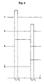
- the set pulse is then put to off at time t 2 .
- the aforementioned oscillating state therefore continues as is and the set state can be maintained.
- the reset pulse is then put to off at time t 4 . Oscillation in the resetting mode then continues as is and the resetting state can be maintained. The operation of returning again to the setting state is the same as described previously and description thereof is omitted.
- single mode light is made to be transmitted by the input/output ports 32 and 33, and it is therefore possible to make the outputted light single mode light.
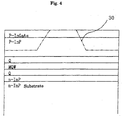
- n-InP is formed to a thickness of 200 nm at the surface (upper surface in FIG. 4) of an n-InP substrate.
- a Q-layer (described later) is then formed to a thickness of 120 nm.
- An MQW layer is then formed thereon to a thickness of 100nm.
- a Q-layer is then formed on top of this to a thickness of 120 nm.
- a P-InP layer is formed to a thickness of 1000 nm.
- a P-InGaAs layer is then formed to a thickness of 200nm on top of this.
- the MQW layer is laminated from five sets of quantum wells of well layer composition: InGaAsP, well layer depth 10 nm, barrier layer composition: same as the Q-layer, and barrier layer thickness 10 nm.
- etching is carried out so as to give the shape shown by the dotted-and-dashed line in FIG. 4.
- a waveguide 30 of the desired shape can then be formed using etching. Namely, the multimode interference portion 31, input port 32 and output port 33 can be formed.
- Width L 1 of multimode interference portion 12 ⁇ m
- Length L 2 of multimode interference portion 570 ⁇ m
- Width L 3 of input/output ports 2 ⁇ m
- FIG. 5(a) shows oscillation conditions in the setting mode
- FIG. 5(b) shows the same in the resetting mode. It can be confirmed that state transitions are made to occur between these modes using input of a set pulse and a reset pulse. Stable oscillation can be confirmed for these modes.
- FIG. 5 portions of high photon density are shown using high brightness.
- FIG. 6 an all-optical flip-flop of a second embodiment of the present invention.
- a mirror 40 for reflecting inputted light is provided at a central part of the multimode interference portion 31. Further, the input/output ports are combined. This is to say that the set port 321 doubles as the inverting output port 332 and the reset port 322 doubles as the non-inverting output port 331.
- the configuration of the waveguide 30 of the first embodiment is substantially folded around to the position of the mirror 40. As a result of doing this, the functions are equivalent to those of the first embodiment. However, it is possible to reduce the size of the device.
- Circulators 50 for sorting inputted/outputted light and allowing inputted/outputted light to pass in prescribed directions are fitted to the input/output ports.
- the functions possessed by the circulators 50 themselves are publicly known. Other aspects of the configuration and operation are the same as for the first embodiment and are not described here.
- a single mode waveguide structure is adopted for the input/output ports 32 and 33 but a multi-mode structure may also be adopted.
- two output ports are provided, but it is also possible to just have one in cases where just one of the inverting output and the non-inverting output are used.
- saturable absorption regions are provided at the input ports, but these may also be provided at the output ports.
- theory of operation is the same as described above.
- the set port 321 and the reset port 322 are next to each other, but the present invention is by no means limited in this respect.
- the position of the inverting output port 332 may also be taken as the position (i.e. a position on the opposite side to the set port 321) of the inverting output port 332 shown in FIG. 2.
- the position of the inverting output port 332 may also be taken to be the position of the setting port 322. Therefore, fundamentally, any position for the input port is appropriate providing that the gain of one mode is lost and oscillation of the other mode is established.
- the position of the output port may be any position enabling extraction of outputted light in a certain mode.
Landscapes
- Physics & Mathematics (AREA)
- General Physics & Mathematics (AREA)
- Nonlinear Science (AREA)
- Optics & Photonics (AREA)
- Optical Modulation, Optical Deflection, Nonlinear Optics, Optical Demodulation, Optical Logic Elements (AREA)
- Semiconductor Lasers (AREA)
- Optical Integrated Circuits (AREA)
Abstract
Description
Width L1 of multimode interference portion: 12 µm
Length L2 of multimode interference portion: 570 µm
Width L3 of input/output ports: 2 µm
Length L4 from end of
Claims (9)
- An all-optical flip-flop comprising a semiconductor laser, the semiconductor laser being equipped with a waveguide, the waveguide being equipped with a multi-mode interference portion, a plurality of input port, and an output port, the input and output ports being connected to the multi-mode interference portion, with configuration being such that a set pulse from one or more input ports and a reset pulse from (a) remaining input port(s) is inputted to the multi-mode interference portion, wherein the multi-mode interference portion transmits multi-mode light within, with light outputted due to oscillation based on the set pulse and the reset pulse inputted from the input ports being selectively outputted from the output port.
- The all-optical flip-flop as disclosed in claim 1, wherein oscillation based on the set pulse and the reset pulse generates different modes according to the set pulse and the reset pulse.
- The all-optical flip-flop as disclosed in claim 1 and claim 2, wherein a plurality of output ports are provided.
- The all-optical flip-flop as disclosed in any one of claims 1 to 3, wherein the input ports and the output ports are capable of allowing single mode light to pass.
- The all-optical flip-flop as disclosed in any one of claims 1 to 4, wherein saturable absorption regions are provided at the input ports and the output ports.
- The all-optical flip-flop as disclosed in any one of claims 1 to 5, wherein end surfaces of the input port and the output port are reflecting surfaces.
- The all-optical flip-flop as disclosed in any one of claims 1 to 6, wherein the input port doubles as the output port.
- The all-optical flip-flop as disclosed in claim 7, wherein a mirror for reflecting inputted light is provided at the multi-mode interference portion.
- The all-optical flip-flop as disclosed in claim 7 or claim 8, wherein circulators for switching over paths for inputted and outputted light are fitted at the input ports doubling as the output ports.
Applications Claiming Priority (3)
| Application Number | Priority Date | Filing Date | Title |
|---|---|---|---|
| JP2001278213A JP3578737B6 (en) | 2001-09-13 | All-optical flip-flop | |
| JP2001278213 | 2001-09-13 | ||
| PCT/JP2002/009238 WO2003025665A1 (en) | 2001-09-13 | 2002-09-10 | All-optical flip-flop |
Publications (3)
| Publication Number | Publication Date |
|---|---|
| EP1437622A1 true EP1437622A1 (en) | 2004-07-14 |
| EP1437622A4 EP1437622A4 (en) | 2005-06-29 |
| EP1437622B1 EP1437622B1 (en) | 2006-11-08 |
Family
ID=19102618
Family Applications (1)
| Application Number | Title | Priority Date | Filing Date |
|---|---|---|---|
| EP02798659A Expired - Lifetime EP1437622B1 (en) | 2001-09-13 | 2002-09-10 | All-optical flip-flop |
Country Status (4)
| Country | Link |
|---|---|
| US (1) | US7292746B2 (en) |
| EP (1) | EP1437622B1 (en) |
| DE (1) | DE60215965T2 (en) |
| WO (1) | WO2003025665A1 (en) |
Cited By (1)
| Publication number | Priority date | Publication date | Assignee | Title |
|---|---|---|---|---|
| EP2527917A4 (en) * | 2010-01-19 | 2014-05-21 | Univ Kyushu Nat Univ Corp | BISTABLE ELEMENT |
Families Citing this family (6)
| Publication number | Priority date | Publication date | Assignee | Title |
|---|---|---|---|---|
| GB2522252B (en) | 2014-01-20 | 2016-04-20 | Rockley Photonics Ltd | Tunable SOI laser |
| US11699892B2 (en) | 2016-02-19 | 2023-07-11 | Rockley Photonics Limited | Discrete wavelength tunable laser |
| GB2547467A (en) | 2016-02-19 | 2017-08-23 | Rockley Photonics Ltd | Tunable laser |
| US12368283B2 (en) | 2017-06-14 | 2025-07-22 | Rockley Photonics Limited | Broadband arbitrary wavelength multichannel laser source |
| US10811848B2 (en) | 2017-06-14 | 2020-10-20 | Rockley Photonics Limited | Broadband arbitrary wavelength multichannel laser source |
| JP7608153B2 (en) | 2020-12-25 | 2025-01-06 | 古河電気工業株式会社 | Optical Devices and Apparatus |
Family Cites Families (16)
| Publication number | Priority date | Publication date | Assignee | Title |
|---|---|---|---|---|
| JPS5125710B1 (en) * | 1964-11-13 | 1976-08-02 | ||
| US3439289A (en) * | 1965-07-08 | 1969-04-15 | Us Air Force | Semiconductor laser components for digital logic |
| JPH04116630A (en) * | 1990-09-07 | 1992-04-17 | Nippon Telegr & Teleph Corp <Ntt> | Optical flip-flop laser |
| JPH0770787B2 (en) * | 1991-09-11 | 1995-07-31 | 工業技術院長 | Semiconductor laser |
| JPH0770786B2 (en) * | 1991-09-11 | 1995-07-31 | 工業技術院長 | Semiconductor laser and operating method thereof |
| JP3062562B2 (en) | 1991-11-06 | 2000-07-10 | 株式会社ブリヂストン | How to lay a water leak detection sheet at an industrial waste treatment plant |
| JPH07225404A (en) * | 1994-02-14 | 1995-08-22 | Oki Electric Ind Co Ltd | Optical bistable element and driving method thereof |
| WO1996013084A1 (en) * | 1994-10-21 | 1996-05-02 | Besse Pierre Andre | Process for controlling saturation and non-linear effects in optical semiconductor amplifiers |
| JPH09186389A (en) * | 1996-01-08 | 1997-07-15 | Nippon Telegr & Teleph Corp <Ntt> | Light control laser switch |
| US5999283A (en) * | 1997-05-19 | 1999-12-07 | Roberts; Kim Byron | Optical logic devices and methods |
| US5999284A (en) * | 1997-06-05 | 1999-12-07 | Northern Telecom Limited | Optical detection and logic devices with latching function |
| JP3244116B2 (en) * | 1997-08-18 | 2002-01-07 | 日本電気株式会社 | Semiconductor laser |
| US6473541B1 (en) * | 1999-09-15 | 2002-10-29 | Seng-Tiong Ho | Photon transistors |
| US6298180B1 (en) * | 1999-09-15 | 2001-10-02 | Seng-Tiong Ho | Photon transistors |
| JP2001166349A (en) * | 1999-12-10 | 2001-06-22 | Sentan Kagaku Gijutsu Incubation Center:Kk | Optical flip-flop device |
| US6522462B2 (en) * | 2001-06-29 | 2003-02-18 | Super Light Wave Corp. | All optical logic using cross-phase modulation amplifiers and mach-zehnder interferometers with phase-shift devices |
-
2002
- 2002-09-10 WO PCT/JP2002/009238 patent/WO2003025665A1/en not_active Ceased
- 2002-09-10 EP EP02798659A patent/EP1437622B1/en not_active Expired - Lifetime
- 2002-09-10 DE DE60215965T patent/DE60215965T2/en not_active Expired - Lifetime
-
2004
- 2004-03-12 US US10/799,786 patent/US7292746B2/en not_active Expired - Fee Related
Cited By (1)
| Publication number | Priority date | Publication date | Assignee | Title |
|---|---|---|---|---|
| EP2527917A4 (en) * | 2010-01-19 | 2014-05-21 | Univ Kyushu Nat Univ Corp | BISTABLE ELEMENT |
Also Published As
| Publication number | Publication date |
|---|---|
| JP3578737B2 (en) | 2004-10-20 |
| DE60215965D1 (en) | 2006-12-21 |
| WO2003025665A1 (en) | 2003-03-27 |
| US7292746B2 (en) | 2007-11-06 |
| JP2003084327A (en) | 2003-03-19 |
| EP1437622B1 (en) | 2006-11-08 |
| DE60215965T2 (en) | 2007-03-01 |
| US20040190562A1 (en) | 2004-09-30 |
| EP1437622A4 (en) | 2005-06-29 |
Similar Documents
| Publication | Publication Date | Title |
|---|---|---|
| Liu et al. | An ultra-small, low-power, all-optical flip-flop memory on a silicon chip | |
| Leijtens | JePPIX: the platform for Indium Phosphide-based photonics | |
| JP5083732B2 (en) | Light switch | |
| JP5721246B1 (en) | Surface emitting laser with light modulation function | |
| WO2011090079A1 (en) | Bistable element | |
| JPS6079786A (en) | Bistable laser | |
| EP1437622B1 (en) | All-optical flip-flop | |
| CN114050473B (en) | Monolithically Integrated Narrow Linewidth Coupled Cavity Semiconductor Laser | |
| CN115207770A (en) | Ultra-high bandwidth and high power direct modulation laser based on light-light resonance effect | |
| Vagionas et al. | All optical flip flop with two coupled travelling waveguide SOA-XGM switches | |
| JP6019522B2 (en) | Surface emitting laser device | |
| JP4868827B2 (en) | Laser guided optical wiring device | |
| CN106933000B (en) | all-optical trigger | |
| JP3578737B6 (en) | All-optical flip-flop | |
| Gibson et al. | GeSn nanobeam light-emitting diode as a GHz-modulated light source | |
| CN206340825U (en) | A kind of mode locking semiconductor laser based on multimode interferometric structure | |
| JPH0340480A (en) | Semiconductor ring laser | |
| Zhang et al. | The design of bi-layer vertical grating coupler for the hybrid integration of VCSEL with stable polarization on silicon photonics | |
| Takeda et al. | All-optical flip-flop based on Mach-Zehnder interferometer bistable laser diode | |
| Takeda et al. | Design and fabrication of Mach-Zehnder interferometer bistable laser diode all-optical flip-flop | |
| Aoki et al. | Demonstration of switchable all-optical flip-flop and inverter operations in semiconductor microring laser | |
| CN106329310A (en) | Mode-locked semiconductor laser based on multimode interference structure | |
| JP2018113302A (en) | Modulated light source and optical module | |
| KR100526545B1 (en) | Distributed feedback laser | |
| JP2015185765A (en) | External resonator laser |
Legal Events
| Date | Code | Title | Description |
|---|---|---|---|
| PUAI | Public reference made under article 153(3) epc to a published international application that has entered the european phase |
Free format text: ORIGINAL CODE: 0009012 |
|
| 17P | Request for examination filed |
Effective date: 20040317 |
|
| AK | Designated contracting states |
Kind code of ref document: A1 Designated state(s): AT BE BG CH CY CZ DE DK EE ES FI FR GB GR IE IT LI LU MC NL PT SE SK TR |
|
| AX | Request for extension of the european patent |
Extension state: AL LT LV MK RO SI |
|
| RTI1 | Title (correction) |
Free format text: ALL-OPTICAL FLIP-FLOP |
|
| A4 | Supplementary search report drawn up and despatched |
Effective date: 20050517 |
|
| RIC1 | Information provided on ipc code assigned before grant |
Ipc: 7G 02F 3/02 B Ipc: 7H 01S 3/082 B Ipc: 7G 02F 3/00 A |
|
| 17Q | First examination report despatched |
Effective date: 20050629 |
|
| GRAP | Despatch of communication of intention to grant a patent |
Free format text: ORIGINAL CODE: EPIDOSNIGR1 |
|
| GRAS | Grant fee paid |
Free format text: ORIGINAL CODE: EPIDOSNIGR3 |
|
| GRAA | (expected) grant |
Free format text: ORIGINAL CODE: 0009210 |
|
| AK | Designated contracting states |
Kind code of ref document: B1 Designated state(s): DE FR GB |
|
| REG | Reference to a national code |
Ref country code: GB Ref legal event code: FG4D |
|
| REF | Corresponds to: |
Ref document number: 60215965 Country of ref document: DE Date of ref document: 20061221 Kind code of ref document: P |
|
| ET | Fr: translation filed | ||
| PLBE | No opposition filed within time limit |
Free format text: ORIGINAL CODE: 0009261 |
|
| STAA | Information on the status of an ep patent application or granted ep patent |
Free format text: STATUS: NO OPPOSITION FILED WITHIN TIME LIMIT |
|
| 26N | No opposition filed |
Effective date: 20070809 |
|
| PGFP | Annual fee paid to national office [announced via postgrant information from national office to epo] |
Ref country code: GB Payment date: 20100827 Year of fee payment: 9 |
|
| PGFP | Annual fee paid to national office [announced via postgrant information from national office to epo] |
Ref country code: FR Payment date: 20101012 Year of fee payment: 9 |
|
| PGFP | Annual fee paid to national office [announced via postgrant information from national office to epo] |
Ref country code: DE Payment date: 20101130 Year of fee payment: 9 |
|
| GBPC | Gb: european patent ceased through non-payment of renewal fee |
Effective date: 20110910 |
|
| REG | Reference to a national code |
Ref country code: FR Ref legal event code: ST Effective date: 20120531 |
|
| REG | Reference to a national code |
Ref country code: DE Ref legal event code: R119 Ref document number: 60215965 Country of ref document: DE Effective date: 20120403 |
|
| PG25 | Lapsed in a contracting state [announced via postgrant information from national office to epo] |
Ref country code: DE Free format text: LAPSE BECAUSE OF NON-PAYMENT OF DUE FEES Effective date: 20120403 |
|
| PG25 | Lapsed in a contracting state [announced via postgrant information from national office to epo] |
Ref country code: GB Free format text: LAPSE BECAUSE OF NON-PAYMENT OF DUE FEES Effective date: 20110910 Ref country code: FR Free format text: LAPSE BECAUSE OF NON-PAYMENT OF DUE FEES Effective date: 20110930 |