EP1437586B1 - Method of measuring the half-wave voltage of a mach-zehnder type optical modulator - Google Patents
Method of measuring the half-wave voltage of a mach-zehnder type optical modulator Download PDFInfo
- Publication number
- EP1437586B1 EP1437586B1 EP02755710A EP02755710A EP1437586B1 EP 1437586 B1 EP1437586 B1 EP 1437586B1 EP 02755710 A EP02755710 A EP 02755710A EP 02755710 A EP02755710 A EP 02755710A EP 1437586 B1 EP1437586 B1 EP 1437586B1
- Authority
- EP
- European Patent Office
- Prior art keywords
- frequency
- optical modulator
- signal
- type optical
- mach
- Prior art date
- Legal status (The legal status is an assumption and is not a legal conclusion. Google has not performed a legal analysis and makes no representation as to the accuracy of the status listed.)
- Expired - Lifetime
Links
- 230000003287 optical effect Effects 0.000 title claims abstract description 67
- 238000000034 method Methods 0.000 title claims description 25
- 238000005259 measurement Methods 0.000 abstract description 13
- 229910003327 LiNbO3 Inorganic materials 0.000 description 10
- 238000012360 testing method Methods 0.000 description 7
- 238000004891 communication Methods 0.000 description 5
- 230000000694 effects Effects 0.000 description 3
- 238000012544 monitoring process Methods 0.000 description 3
- 238000005070 sampling Methods 0.000 description 2
- 239000000758 substrate Substances 0.000 description 2
- 230000001419 dependent effect Effects 0.000 description 1
- 238000002474 experimental method Methods 0.000 description 1
- 239000013307 optical fiber Substances 0.000 description 1
- 230000005693 optoelectronics Effects 0.000 description 1
- 238000001228 spectrum Methods 0.000 description 1
Images



Classifications
-
- G—PHYSICS
- G02—OPTICS
- G02F—OPTICAL DEVICES OR ARRANGEMENTS FOR THE CONTROL OF LIGHT BY MODIFICATION OF THE OPTICAL PROPERTIES OF THE MEDIA OF THE ELEMENTS INVOLVED THEREIN; NON-LINEAR OPTICS; FREQUENCY-CHANGING OF LIGHT; OPTICAL LOGIC ELEMENTS; OPTICAL ANALOGUE/DIGITAL CONVERTERS
- G02F1/00—Devices or arrangements for the control of the intensity, colour, phase, polarisation or direction of light arriving from an independent light source, e.g. switching, gating or modulating; Non-linear optics
- G02F1/01—Devices or arrangements for the control of the intensity, colour, phase, polarisation or direction of light arriving from an independent light source, e.g. switching, gating or modulating; Non-linear optics for the control of the intensity, phase, polarisation or colour
- G02F1/0121—Operation of devices; Circuit arrangements, not otherwise provided for in this subclass
- G02F1/0123—Circuits for the control or stabilisation of the bias voltage, e.g. automatic bias control [ABC] feedback loops
-
- G—PHYSICS
- G02—OPTICS
- G02F—OPTICAL DEVICES OR ARRANGEMENTS FOR THE CONTROL OF LIGHT BY MODIFICATION OF THE OPTICAL PROPERTIES OF THE MEDIA OF THE ELEMENTS INVOLVED THEREIN; NON-LINEAR OPTICS; FREQUENCY-CHANGING OF LIGHT; OPTICAL LOGIC ELEMENTS; OPTICAL ANALOGUE/DIGITAL CONVERTERS
- G02F1/00—Devices or arrangements for the control of the intensity, colour, phase, polarisation or direction of light arriving from an independent light source, e.g. switching, gating or modulating; Non-linear optics
- G02F1/01—Devices or arrangements for the control of the intensity, colour, phase, polarisation or direction of light arriving from an independent light source, e.g. switching, gating or modulating; Non-linear optics for the control of the intensity, phase, polarisation or colour
- G02F1/21—Devices or arrangements for the control of the intensity, colour, phase, polarisation or direction of light arriving from an independent light source, e.g. switching, gating or modulating; Non-linear optics for the control of the intensity, phase, polarisation or colour by interference
- G02F1/225—Devices or arrangements for the control of the intensity, colour, phase, polarisation or direction of light arriving from an independent light source, e.g. switching, gating or modulating; Non-linear optics for the control of the intensity, phase, polarisation or colour by interference in an optical waveguide structure
-
- G—PHYSICS
- G02—OPTICS
- G02F—OPTICAL DEVICES OR ARRANGEMENTS FOR THE CONTROL OF LIGHT BY MODIFICATION OF THE OPTICAL PROPERTIES OF THE MEDIA OF THE ELEMENTS INVOLVED THEREIN; NON-LINEAR OPTICS; FREQUENCY-CHANGING OF LIGHT; OPTICAL LOGIC ELEMENTS; OPTICAL ANALOGUE/DIGITAL CONVERTERS
- G02F1/00—Devices or arrangements for the control of the intensity, colour, phase, polarisation or direction of light arriving from an independent light source, e.g. switching, gating or modulating; Non-linear optics
- G02F1/01—Devices or arrangements for the control of the intensity, colour, phase, polarisation or direction of light arriving from an independent light source, e.g. switching, gating or modulating; Non-linear optics for the control of the intensity, phase, polarisation or colour
- G02F1/0121—Operation of devices; Circuit arrangements, not otherwise provided for in this subclass
Definitions
- Present invention relates to a method of measuring the half-wave voltage (AC half-wave voltage) of a Mach-Zehnder type optical modulator (hereinafter refer to as MZ type optical modulator), especially a method of measuring the half-wave voltage at high frequency of a MZ type optical modulator, which corresponds to high frequency modulation used in high-speed and high-capacity optical fiber communications.
- MZ type optical modulator Mach-Zehnder type optical modulator
- An optical modulator is the primary element, which is used in transmitting parts of optical communications, especially, in recent high-speed and high-capacity optical communication, MZ type optical modulator, which is made by using LiNbO 3 (LN) is used in huge range with its features such as high-speed, wide wavelength band, and low-chirp.
- MZ type optical modulator which is made by using LiNbO 3 (LN) is used in huge range with its features such as high-speed, wide wavelength band, and low-chirp.
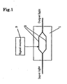
- MZ type optical modulator 1 is composed of light guide 2 which is for guiding light waves, on the substrate that has an electro-optical effect , and the electrodes (not shown) which is for applying high-speed modulation signal of micro wave band to said light waves, and so on.
- the principle of MZ type optical modulator's operation is that the input light from one end of the light guide 2 is divided on the way and because the lights pass inside the substrate of which the refractive index has changed dependent on the amount of electronic signal voltage which applied from signal source, speed difference occurs between mutual divided lights, and as the two divided lights converge, phase difference occurs, and the combined output light shows an intensity change which respond to said electronic signal.
- the figure 2 shows the change of output light (I) in relation to the change of input voltage (V) of signal source 3 which is applied to MZ type optical modulator 1, and generally, as the input voltage V increases, light output I draw a curve that vibrates as a sine wave in certain range.
- V ⁇ an input voltage range between minimum point and maximum point of the light output
- V ⁇ is important to determine the voltage of electronic signal which is applied to optical modulator.
- figure 3 which shows the way to observe the light output directly (prior art example 1)
- figure 5 shown in United States Patent No.6204954 which is a method using the average power of output light (prior art example 2).
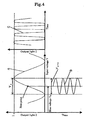
- the method for measuring by prior art example 1 is that when the relation between input voltage V and output light I (V-I characteristic) of MZ type optical modulator 1 is like graph A in figure 4, if bias voltage V B is superimposed to high-frequency AC signal which has peak-peak voltage amplitude value Vp-p and input voltage as graph B is applied to MZ type optical modulator 1, output light becomes like graph C, and the wave form of graph C is observed directly on sampling oscilloscope 52.
- V ⁇ V p-p
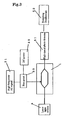
- the voltage of high-frequency AC signal 31 superposed with bias voltage from DC power 32 by bias T 33 is applied to the MZ type optical modulator 1 which the laser is passing through. Then it is comprised to diverge the light from MZ type optical modulator 1 at light coupler 53, to detect one light by light power meter 54 and another light by photo detector 55, and to introduce the detected power of the photo detector to spectrum analyzer 56.
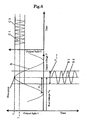
- the method of measuring by the prior art example 2 is that when relationship between input voltage V and light output I (V-I characteristics) of MZ type optical modulator 1 shows the pattern like graph A in figure 6, after adjusting the bias voltage V B to the input voltage showing peak volume in graph A of V-I characteristic (bias point adjustment), it is carried out to measure average power volume of light output (graph C1) in the case (graph B1) of superposing high-frequency AC signal which has peak-peak voltage amplitude volume V p-p to bias voltage V B , light output volume (graph C2) in not adding high-frequency AC signal (only bias voltage V B , graph B2), and V p-p of high-frequency AC signal. Then by using that the V-I characteristic becomes to sine function, it is possible to find out half-wave voltage V ⁇ of MZ type optical modulator.
- Present invention solves these problems and offers a method of measuring that is able to measure half-wave voltage of MZ type optical modulator accurately at high-frequency, does not depend on the bias point variation of the optical modulator, and in which the parameters for calculation are simple.
- an output light of M-Z type optical modulator 1 can be indicated as formula 1.
- I 0 represents the maximum value of output light
- V p-p means the peak-peak voltage amplitude value of high-frequency AC signal 34
- f is the frequency of the high-frequency AC signal 34 which is frequency under test
- V ⁇ means the half-wave voltage of MZ type optical modulator 1 at frequency f under test.
- the low-speed response I' of output light I is equivalent to take time average of high-frequency AC signal (frequency f), and enables to be expressed as formula 2.
- the low-speed response I' of output light of MZ type optical modulator can be expressed in product of constant term, Bessel function at 0 order, and cosine function.
- the amount expressed as Bessel function is the change in output light caused by high-frequency AC signal 34
- the amount expressed as cosine function is the change in output light caused by low-frequency AC signal 35.
- 1.55 ⁇ m laser light from laser light source is entered to MZ type LN optical modulator 11 with adjusting the condition of polarized wave by passing polarized wave controller 42.
- High-frequency AC signal at frequency f under test and monitoring low-frequency AC signal is entered in a superimposed manner to LN optical modulator 11.
- An input of high-frequency AC signal is that high-frequency micro wave from high-frequency signal generator 34-1, in changing the voltage amplitude value of said micro wave by high-frequency amplifier 34-2 , is entered to high-frequency RF port of LN optical modulator 11.
- An input of low-frequency AC signal is that 1 kHz sine wave from low-frequency signal generator 35-1 is entered to BIAS port of LN optical modulator 11.
- the output light from LN optical modulator 11 is detected by photo detector 57 and the detector signal is observed by oscilloscope 58.
- the measurements results of the present invention are that for each frequency under test were 1GHz, 5GHz, 10GHz, half-wave voltage were 4.9V, 5.7V, 6.4V.
- Figure 10 is a graph that compares the characteristics of electrical and optical response of LN optical modulator 11 by using half-wave voltage of these measurement results, with measurements of characteristics of electrical and optical response of LN optical modulator 11 by using a light component analyzer. According to this graph, both results match very closely, and although the measurement of present invention is much simplified compared to usual way, the results catch characteristics of LN optical modulator 11 appropriately, which means that the measurement accuracy of the present invention is extremely fine.
- the method of present the invention is able to automate, for instance, it is able to make up to increase voltage amplitude V p-p of high-frequency AC signal from 0 automatically, store a value of V p-p at the point when fluctuation range of low-speed response I' of output light become within a set value ( The more the set value is near 0, the more measurement result becomes accurate. But it is difficult to make it 0 because of the effect of measurement error, so it is desirable to set the value for carrying out effective measurements as usage of measurement results), and calculate half-wave voltage V ⁇ by using the value of V p-p in operational equipment which set up separately. Then, by carrying out same method of measuring with changing the frequency under test sequentially, it is possible to measure half-wave voltage over any frequency band automatically.
- V p-pmin is needed as a parameter to calculate half-wave voltage V ⁇ , therefore it is possible to offer extremely effective method of measuring the half-wave voltage of a Mach-Zehnder type optical modulator.
Landscapes
- Physics & Mathematics (AREA)
- Nonlinear Science (AREA)
- General Physics & Mathematics (AREA)
- Optics & Photonics (AREA)
- Testing Of Optical Devices Or Fibers (AREA)
- Optical Modulation, Optical Deflection, Nonlinear Optics, Optical Demodulation, Optical Logic Elements (AREA)
- Measuring Instrument Details And Bridges, And Automatic Balancing Devices (AREA)
- Photometry And Measurement Of Optical Pulse Characteristics (AREA)
- Optical Communication System (AREA)
- Measurement Of Current Or Voltage (AREA)
Abstract
Description
- Present invention relates to a method of measuring the half-wave voltage (AC half-wave voltage) of a Mach-Zehnder type optical modulator (hereinafter refer to as MZ type optical modulator), especially a method of measuring the half-wave voltage at high frequency of a MZ type optical modulator, which corresponds to high frequency modulation used in high-speed and high-capacity optical fiber communications.
- An optical modulator is the primary element, which is used in transmitting parts of optical communications, especially, in recent high-speed and high-capacity optical communication, MZ type optical modulator, which is made by using LiNbO3 (LN) is used in huge range with its features such as high-speed, wide wavelength band, and low-chirp.
- As shown in figure 1, MZ type
optical modulator 1 is composed oflight guide 2 which is for guiding light waves, on the substrate that has an electro-optical effect , and the electrodes (not shown) which is for applying high-speed modulation signal of micro wave band to said light waves, and so on. The principle of MZ type optical modulator's operation is that the input light from one end of thelight guide 2 is divided on the way and because the lights pass inside the substrate of which the refractive index has changed dependent on the amount of electronic signal voltage which applied from signal source, speed difference occurs between mutual divided lights, and as the two divided lights converge, phase difference occurs, and the combined output light shows an intensity change which respond to said electronic signal. - The figure 2 shows the change of output light (I) in relation to the change of input voltage (V) of
signal source 3 which is applied to MZ typeoptical modulator 1, and generally, as the input voltage V increases, light output I draw a curve that vibrates as a sine wave in certain range. As in figure 2, an input voltage range between minimum point and maximum point of the light output is called half-wave voltage VΠ, and when ON/OFF switching control using optical modulator in optical communication is handled, the value VΠ is important to determine the voltage of electronic signal which is applied to optical modulator. - Even when the same optical modulator is used, half-wave voltage changes according to the electronic signal frequency which is applied to optical modulator, and also, as optical communication become high-speed and high-capacity recently, drive frequency of optical modulator has also become high, so it is required to measure accurate half-wave voltage at 10GHz or higher frequency.
- To measure half-wave voltage, there are several methods such as figure 3 which shows the way to observe the light output directly (prior art example 1), or as the figure 5 shown in United States Patent No.6204954 which is a method using the average power of output light (prior art example 2).
- In the prior art example 1, as shown in figure 3, light from
laser source 4 enters to MZ typeoptical modulator 1, and at the same time, the voltage which superimposed bias voltage frombias DC power 32 to high-frequency AC signal 31 by using bias T 33 is applied to MZ typeoptical modulator 1. Then the light from MZ typeoptical modulator 1 is detected by using high-speed photo detector 51, and by observing the detected power on sampling oscilloscope 52, half-wave voltage is measured. - The method for measuring by prior art example 1 is that when the relation between input voltage V and output light I (V-I characteristic) of MZ type
optical modulator 1 is like graph A in figure 4, if bias voltage VB is superimposed to high-frequency AC signal which has peak-peak voltage amplitude value Vp-p and input voltage as graph B is applied to MZ typeoptical modulator 1, output light becomes like graph C, and the wave form of graph C is observed directly on sampling oscilloscope 52. - As carrying this direct observation, by adjusting the voltage value of Vp-p and VB to make peak-peak amplitude of graph C maximum and measuring Vp-p at its peak, half-wave voltage VΠ of MZ type
optical modulator 1 will be determined (VΠ=Vp-p). - However, with the method of measuring by prior art example 1, it is hard to observe an accurate light waveform (graph C in figure 4) at high-frequency over 10GHz, because of the problem with frequency characteristics of light receiving system such as high-speed photo detector 51. Therefore, it cannot measure half-wave voltage precisely.
- On the other hand, in the prior art example 2, as shown in figure 5, the voltage of high-frequency AC signal 31 superposed with bias voltage from
DC power 32 by bias T 33, is applied to the MZ typeoptical modulator 1 which the laser is passing through. Then it is comprised to diverge the light from MZ typeoptical modulator 1 at light coupler 53, to detect one light by light power meter 54 and another light by photo detector 55, and to introduce the detected power of the photo detector to spectrum analyzer 56. - The method of measuring by the prior art example 2 is that when relationship between input voltage V and light output I (V-I characteristics) of MZ type
optical modulator 1 shows the pattern like graph A in figure 6, after adjusting the bias voltage VB to the input voltage showing peak volume in graph A of V-I characteristic (bias point adjustment), it is carried out to measure average power volume of light output (graph C1) in the case (graph B1) of superposing high-frequency AC signal which has peak-peak voltage amplitude volume Vp-p to bias voltage VB, light output volume (graph C2) in not adding high-frequency AC signal (only bias voltage VB, graph B2), and Vp-p of high-frequency AC signal. Then by using that the V-I characteristic becomes to sine function, it is possible to find out half-wave voltage VΠ of MZ type optical modulator. - Handling with the method of measuring by the prior art example 2, it is able to measure an accurate half-wave voltage at high-frequency, but the bias point adjustment for MZ type optical modulator is necessary and there is a problem that an accurate half-wave voltage measurement is difficult when there is a fluctuation in output light because of the bias point variation.
Also, there are many parameters to use for half-wave voltage calculation so the calculation is becoming cumbersome and complicated. - Present invention solves these problems and offers a method of measuring that is able to measure half-wave voltage of MZ type optical modulator accurately at high-frequency, does not depend on the bias point variation of the optical modulator, and in which the parameters for calculation are simple.
- The problems above are solved by the method of measuring the half-wave voltage of a Mach-Zehnder type optical modulator as defined in the appended claims.
-
- Figure 1 is a diagrammatic illustration of a Mach-Zehnder type optical modulator.
- Figure 2 is a graph, which shows the V-I characteristic of a Mach-Zehnder type optical modulator.
- Figure 3 is a diagrammatic illustration, which shows the measuring method according to prior art example 1.
- Figure 4 is a graph, which shows several relations such as V-I characteristic related to the measuring method of the prior art example 1.
- Figure 5 is a diagrammatic illustration, which shows the measuring method according to prior art example 2.
- Figure 6 is a graph, which shows several relations such as V-I characteristic related to the measuring method of the prior art example 2.
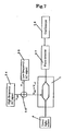
- Figure 7 is a diagrammatic illustration, which shows an experimental setup for carrying out the measuring method of the present invention.
- Figure 8 is a graph, which shows a change in the low-speed response of the output light intensity according to the measuring method of the present invention.
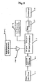
- Figure 9 is a diagrammatic illustration, which shows an other experimental setup for carrying out the measuring method of the present invention.
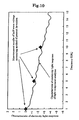
- Figure 10 is a graph, which shows the characteristics of the electro-optical response of a MZ type optical modulator measured by using the method of the present invention.
- Hereinafter, the present invention will be concretely described with preferred examples, but the scope of the present invention is not restricted to these preferred examples.
- In the present invention, as shown in figure 7, after applying a high-frequency AC signal 34 and a monitoring low-frequency AC signal 35 in a superimposed manner to MZ type
optical modulator 1, or as shown in figure 9, after applying the both respectively to separately constituted electrodes (in concrete terms, RF signal electrode and bias port earth electrode), by observing the low-speed response (the change related to low-frequency AC signal 35) of an output light from theoptical modulator 1 by photo detector 57 and oscilloscope 58, and adjusting the voltage amplitude of the high-frequency AC signal 34 in accordance with this observation of the waveform, it makes possible to measure the half-wave voltage of MZ typeoptical modulator 1. - With the present invention, there is no need to adjust or control bias points, which cause a problem for measuring of MZ type optical modulator, and in addition, it becomes possible to measure accurate half-wave voltage very easily.
- The measurement principle of the present invention will be described in the following sentences.
- If a phase change by high-frequency AC signal 34 is Φ1 and a phase change by low-frequency AC signal 35 is Φ2, then an output light of M-Z type
optical modulator 1 can be indicated asformula 1. I0 represents the maximum value of output light, Vp-p means the peak-peak voltage amplitude value of high-frequency AC signal 34, f is the frequency of the high-frequency AC signal 34 which is frequency under test, VΠ means the half-wave voltage of MZ typeoptical modulator 1 at frequency f under test.
- In the next place, the low-speed response I' of output light I is equivalent to take time average of high-frequency AC signal (frequency f), and enables to be expressed as
formula 2.
- Moreover, after expansion into series,
formula 2 turns toformula 3.
- From
formula 3, the low-speed response I' of output light of MZ type optical modulator can be expressed in product of constant term, Bessel function at 0 order, and cosine function. At this point, the amount expressed as Bessel function is the change in output light caused by high-frequency AC signal 34, and the amount expressed as cosine function is the change in output light caused by low-frequency AC signal 35. - Now, if high-frequency AC signal 34 with voltage Vp-p which makes a number of terms of Bessel
function 0 is input, the second term offormula 3 becomes 0, and though any low-frequency AC signal 35 is input, low-speed response I' of output light becomes Io/2 which is fixed output light. Figure 8 (b) shows this situation. - In other words, as changing continuously the voltage amplitude of high-frequency AC signal 34, which puts in MZ type
optical modulator 1 , in observing low-speed response of output light from MZ typeoptical modulator 1 by oscilloscope 58, when a state of the output light that is changing by the effect of low-frequency AC signal as figure 8 (a) becomes constant as shown in figure 8 (b), measuring voltage Vp-p of high-frequency AC signal 34 which is input in MZ typeoptical modulator 1 makes possible to calculate the half-wave voltage VΠ at frequency under test. - The relationship between Vp-p and Vn in the case which the low-speed response I' of output light becomes constant can be derived from the condition which make Bessel function's term of
formula 3 0, that is
- However, because there are several conditions in that Bessel function at 0 order becomes 0, normally for minimizing necessary signal voltage, by using the peak-peak voltage amplitude value Vp-pmin when output light becomes minimum at first, half-wave voltage value VΠ is calculated from the relation ΠVp.pmin/(2VΠ)=2.405.
- One example of experiments on the present invention is shown in figure 9 and figure 10.
- 1.55µm laser light from laser light source is entered to MZ type LN
optical modulator 11 with adjusting the condition of polarized wave by passing polarized wave controller 42. - High-frequency AC signal at frequency f under test and monitoring low-frequency AC signal is entered in a superimposed manner to LN
optical modulator 11. An input of high-frequency AC signal is that high-frequency micro wave from high-frequency signal generator 34-1, in changing the voltage amplitude value of said micro wave by high-frequency amplifier 34-2 , is entered to high-frequency RF port of LNoptical modulator 11. An input of low-frequency AC signal is that 1 kHz sine wave from low-frequency signal generator 35-1 is entered to BIAS port of LNoptical modulator 11. By setting voltage amplitude of low-frequency AC signal for more than double the half-wave voltage, the amplitude value of output light will be the maximum at any time, so the observation become easy and it makes possible to measure in much higher precision. - The output light from LN
optical modulator 11 is detected by photo detector 57 and the detector signal is observed by oscilloscope 58. - The measurements results of the present invention are that for each frequency under test were 1GHz, 5GHz, 10GHz, half-wave voltage were 4.9V, 5.7V, 6.4V.
- Figure 10 is a graph that compares the characteristics of electrical and optical response of LN
optical modulator 11 by using half-wave voltage of these measurement results, with measurements of characteristics of electrical and optical response of LNoptical modulator 11 by using a light component analyzer. According to this graph, both results match very closely, and although the measurement of present invention is much simplified compared to usual way, the results catch characteristics of LNoptical modulator 11 appropriately, which means that the measurement accuracy of the present invention is extremely fine. - Furthermore, the method of present the invention is able to automate, for instance, it is able to make up to increase voltage amplitude Vp-p of high-frequency AC signal from 0 automatically, store a value of Vp-p at the point when fluctuation range of low-speed response I' of output light become within a set value ( The more the set value is near 0, the more measurement result becomes accurate. But it is difficult to make it 0 because of the effect of measurement error, so it is desirable to set the value for carrying out effective measurements as usage of measurement results), and calculate half-wave voltage VΠ by using the value of Vp-p in operational equipment which set up separately. Then, by carrying out same method of measuring with changing the frequency under test sequentially, it is possible to measure half-wave voltage over any frequency band automatically.
- According to the present invention, only by measuring the minimum value Vp-pmin of the voltage amplitude of the high-frequency AC signal when the intensity change of an output light related to the monitoring low-frequency AC signal is almost zero, and substituting it for the formula ΠVp-pmin/(2VΠ)=2.405, half-wave voltage VΠ of Mach-Zehnder type optical modulator can be measured easily.
- In addition, if frequency under test is high frequency, because there is no need to observe high-frequency waveform directly, accurate measurement is possible, and at the same time, because this is not a measuring method which depend on a bias point, there is no need to adjust bias point, and there is no effect from bias point variation of optical modulator.
- Furthermore, only Vp-pmin is needed as a parameter to calculate half-wave voltage VΠ, therefore it is possible to offer extremely effective method of measuring the half-wave voltage of a Mach-Zehnder type optical modulator.
Claims (2)
- A method of measuring the half-wave voltage of a Mach-Zehnder type optical modulator (1) at a predetermined high-frequency comprising the steps of;
superimposing a first AC signal (34) of said predetermined high frequency and a second AC signal (35) of a low frequency to form a composed signal and applying said composed signal to one electrode of said Mach-Zehnder type optical modulator (1)
or
applying a first AC signal (34) of said predetermined high frequency to a first electrode of said Mach-Zehnder type optical modulator (1) and a second AC signal (35) of a low frequency to a second separately constituted electrode of said Mach-Zehnder type optical modulator (1);
inputting light into said Mach-Zehnder type optical modulator (1) ;
outputting light from said Mach-Zehnder type optical modulator (1) ;
detecting the low-frequency changes of the output light intensity due to the low-frequency AC signal (35);
characterized in that
the voltage amplitude of said high-frequency AC signal (34) is varied in order to detect a specific peak-to-peak voltage amplitude value Vp-p of the high-frequency AC signal (34) at which the amplitude of the detected low-frequency changes of the output light intensity is almost zero. - The method of measuring the half-wave voltage of a Mach-Zehnder type optical modulator (1) as claimed in claim 1, wherein, when the amplitude of the detected low-frequency changes of the output light intensity is almost zero, the relationship between the specific peak-to-peak voltage amplitude value Vp-p of said high-frequency AC signal and the half-wave voltage value VΠ of the Mach-Zehnder type optical modulator satisfies the relation

Applications Claiming Priority (3)
| Application Number | Priority Date | Filing Date | Title |
|---|---|---|---|
| JP2001243816 | 2001-08-10 | ||
| JP2001243816A JP4608149B2 (en) | 2001-08-10 | 2001-08-10 | Method and apparatus for measuring half-wave voltage of Mach-Zehnder type optical modulator |
| PCT/JP2002/007784 WO2003016853A1 (en) | 2001-08-10 | 2002-07-31 | Method and device for measuring half-wave voltage of mach-zehnder type optical modulator |
Publications (3)
| Publication Number | Publication Date |
|---|---|
| EP1437586A1 EP1437586A1 (en) | 2004-07-14 |
| EP1437586A4 EP1437586A4 (en) | 2006-05-10 |
| EP1437586B1 true EP1437586B1 (en) | 2007-05-30 |
Family
ID=19073849
Family Applications (1)
| Application Number | Title | Priority Date | Filing Date |
|---|---|---|---|
| EP02755710A Expired - Lifetime EP1437586B1 (en) | 2001-08-10 | 2002-07-31 | Method of measuring the half-wave voltage of a mach-zehnder type optical modulator |
Country Status (8)
| Country | Link |
|---|---|
| US (1) | US7142309B2 (en) |
| EP (1) | EP1437586B1 (en) |
| JP (1) | JP4608149B2 (en) |
| CN (1) | CN1247976C (en) |
| AT (1) | ATE363649T1 (en) |
| CA (1) | CA2456914C (en) |
| DE (1) | DE60220431T2 (en) |
| WO (1) | WO2003016853A1 (en) |
Families Citing this family (11)
| Publication number | Priority date | Publication date | Assignee | Title |
|---|---|---|---|---|
| JP2005127783A (en) * | 2003-10-22 | 2005-05-19 | Yokogawa Electric Corp | Electric signal observation apparatus and method, and electric signal sampling apparatus and method |
| US7805026B2 (en) * | 2007-10-09 | 2010-09-28 | Alcatel-Lucent Usa Inc. | Resonator-assisted control of radio-frequency response in an optical modulator |
| US8014676B2 (en) * | 2008-02-22 | 2011-09-06 | Alcatel Lucent | CMOS-compatible tunable microwave photonic band-stop filter |
| CN101621329B (en) * | 2008-07-03 | 2013-01-23 | 华为技术有限公司 | Method and system for measuring bias points of double-parallel modulator |
| JP5622154B2 (en) * | 2009-09-07 | 2014-11-12 | 独立行政法人情報通信研究機構 | Evaluation method of optical modulator with multiple Mach-Zehnder interferometers |
| CN102798750B (en) * | 2012-08-17 | 2015-04-29 | 华中科技大学 | Method and system for measuring half-wave voltage of electro-optical modulator |
| US10684311B2 (en) * | 2017-05-10 | 2020-06-16 | Tektronix, Inc. | High input impedance electro-optic sensor |
| CN111707361B (en) * | 2020-06-28 | 2023-04-11 | 中国电子科技集团公司第四十四研究所 | Method for measuring half-wave voltage of M-Z type light intensity modulator |
| CN111707360B (en) * | 2020-06-28 | 2023-03-31 | 中国电子科技集团公司第四十四研究所 | Method for measuring half-wave voltage of M-Z type light intensity modulator |
| CN114689921B (en) * | 2020-12-30 | 2026-03-10 | 科大国盾量子技术股份有限公司 | Device and method for measuring half-wave voltage of phase modulator |
| CN114362822B (en) * | 2021-12-08 | 2023-08-22 | 中国人民解放军战略支援部队信息工程大学 | Based on LiNbO 3 Natural light communication method of body modulator |
Family Cites Families (9)
| Publication number | Priority date | Publication date | Assignee | Title |
|---|---|---|---|---|
| JP2939482B2 (en) * | 1989-10-06 | 1999-08-25 | 日本電信電話株式会社 | Apparatus and method for measuring characteristics of optical phase modulator |
| JPH03139653A (en) * | 1989-10-26 | 1991-06-13 | Fuji Photo Film Co Ltd | Original plate for electrophotographic type planographic printing |
| JP2792482B2 (en) * | 1995-09-28 | 1998-09-03 | 日本電気株式会社 | Semiconductor Mach-Zehnder modulator |
| JPH10148801A (en) * | 1996-11-21 | 1998-06-02 | Toshiba Corp | Optical modulation device using external modulation method |
| JP3913856B2 (en) * | 1997-08-28 | 2007-05-09 | 富士通株式会社 | Optical pulse generation device, dispersion measurement device, dispersion compensation device, and dispersion measurement method |
| US6204954B1 (en) * | 1999-09-22 | 2001-03-20 | Nortel Networks Limited | Technique for measuring the Vpi-AC of a mach-zehnder modulator |
| JP2001154164A (en) * | 1999-11-25 | 2001-06-08 | Nec Corp | Optical modulator and optical modulation method |
| JP3693872B2 (en) * | 1999-12-02 | 2005-09-14 | 住友大阪セメント株式会社 | Light modulation apparatus and method |
| US6956653B1 (en) * | 2000-06-27 | 2005-10-18 | Lockheed Martin Corporation | Dual electrooptic waveguide interferometer |
-
2001
- 2001-08-10 JP JP2001243816A patent/JP4608149B2/en not_active Expired - Fee Related
-
2002
- 2002-07-31 US US10/486,610 patent/US7142309B2/en not_active Expired - Fee Related
- 2002-07-31 CA CA2456914A patent/CA2456914C/en not_active Expired - Fee Related
- 2002-07-31 WO PCT/JP2002/007784 patent/WO2003016853A1/en not_active Ceased
- 2002-07-31 AT AT02755710T patent/ATE363649T1/en not_active IP Right Cessation
- 2002-07-31 CN CNB028154800A patent/CN1247976C/en not_active Expired - Fee Related
- 2002-07-31 EP EP02755710A patent/EP1437586B1/en not_active Expired - Lifetime
- 2002-07-31 DE DE60220431T patent/DE60220431T2/en not_active Expired - Lifetime
Non-Patent Citations (1)
| Title |
|---|
| None * |
Also Published As
| Publication number | Publication date |
|---|---|
| CN1247976C (en) | 2006-03-29 |
| ATE363649T1 (en) | 2007-06-15 |
| DE60220431D1 (en) | 2007-07-12 |
| JP2003057615A (en) | 2003-02-26 |
| EP1437586A1 (en) | 2004-07-14 |
| CN1539078A (en) | 2004-10-20 |
| US7142309B2 (en) | 2006-11-28 |
| CA2456914A1 (en) | 2003-02-27 |
| US20040247219A1 (en) | 2004-12-09 |
| EP1437586A4 (en) | 2006-05-10 |
| JP4608149B2 (en) | 2011-01-05 |
| WO2003016853A1 (en) | 2003-02-27 |
| CA2456914C (en) | 2011-04-12 |
| DE60220431T2 (en) | 2008-03-13 |
Similar Documents
| Publication | Publication Date | Title |
|---|---|---|
| US6323950B1 (en) | Chromatic dispersion measurement for optical components | |
| CN102706540B (en) | System for measuring half-wave voltage of phase modulator and measurement method | |
| JP2866186B2 (en) | Electromagnetic field strength measuring device | |
| EP2541307A1 (en) | Optical frequency comb generating device and optical pulse generating device using same, and optical frequency comb generating method and optical pulse generating method using same | |
| CN110017967B (en) | A method for measuring chirp parameters of electro-optical intensity modulators based on phase comparison | |
| CN106301554B (en) | A debugging method and debugging device for operating point voltage of a parallel MZI electro-optical modulator | |
| US6204954B1 (en) | Technique for measuring the Vpi-AC of a mach-zehnder modulator | |
| EP1437586A1 (en) | Method and device for measuring half-wave voltage of mach-zehnder type optical modulator | |
| JP2619981B2 (en) | Electromagnetic field strength measuring device | |
| JPH0460464A (en) | Narrow spectrum short pulse light source apparatus and voltage detector | |
| EP2309323B1 (en) | Method for evaluating characteristics of an optical modulator including plural mach-zehnder interferometers | |
| CN110411715B (en) | Device and method for determining half-wave voltage of AMZI phase modulator | |
| US7239396B2 (en) | Method and apparatus for directly measuring the phase change of an optical signal | |
| EP2477021A1 (en) | Method for evaluating characteristic of optical modulator having mach-zehnder interferometer | |
| CN1664538A (en) | On-line test method and test device for integrated optical modulator for fiber optic gyroscope | |
| US20080297768A1 (en) | Polarization Mode Dispersion Analyzer | |
| CN106443126A (en) | Method and device for measuring half-wave voltage of electro-optical crystal | |
| EP2251666A1 (en) | Method for evaluating characteristics of optical modulator having high-precision mach-zehnder interferometer | |
| US4982151A (en) | Voltage measuring apparatus | |
| CN209930266U (en) | A test device for unequal arm interferometer based on intensity modulation | |
| CN106124857B (en) | A Microwave Photonics Frequency Measurement Device Based on Electro-Optical Perspective Cavity | |
| CN113589019B (en) | Simplified measurement device and method for half-wave voltage of optical phase modulator | |
| JP3866082B2 (en) | Method and apparatus for measuring characteristics of optical modulator | |
| EP4489329A1 (en) | Apparatus and method for measuring chirp in fiber optical transmitters | |
| CN114062276A (en) | Temperature self-compensation method and device for optical fiber photoacoustic sensing |
Legal Events
| Date | Code | Title | Description |
|---|---|---|---|
| PUAI | Public reference made under article 153(3) epc to a published international application that has entered the european phase |
Free format text: ORIGINAL CODE: 0009012 |
|
| 17P | Request for examination filed |
Effective date: 20040226 |
|
| AK | Designated contracting states |
Kind code of ref document: A1 Designated state(s): AT BE BG CH CY CZ DE DK EE ES FI FR GB GR IE IT LI LU MC NL PT SE SK TR |
|
| A4 | Supplementary search report drawn up and despatched |
Effective date: 20060323 |
|
| GRAP | Despatch of communication of intention to grant a patent |
Free format text: ORIGINAL CODE: EPIDOSNIGR1 |
|
| RTI1 | Title (correction) |
Free format text: METHOD OF MEASURING THE HALF-WAVE VOLTAGE OF A MACH-ZEHNDER TYPE OPTICAL MODULATOR |
|
| GRAS | Grant fee paid |
Free format text: ORIGINAL CODE: EPIDOSNIGR3 |
|
| GRAA | (expected) grant |
Free format text: ORIGINAL CODE: 0009210 |
|
| AK | Designated contracting states |
Kind code of ref document: B1 Designated state(s): AT BE BG CH CY CZ DE DK EE ES FI FR GB GR IE IT LI LU MC NL PT SE SK TR |
|
| PG25 | Lapsed in a contracting state [announced via postgrant information from national office to epo] |
Ref country code: FI Free format text: LAPSE BECAUSE OF FAILURE TO SUBMIT A TRANSLATION OF THE DESCRIPTION OR TO PAY THE FEE WITHIN THE PRESCRIBED TIME-LIMIT Effective date: 20070530 Ref country code: CH Free format text: LAPSE BECAUSE OF FAILURE TO SUBMIT A TRANSLATION OF THE DESCRIPTION OR TO PAY THE FEE WITHIN THE PRESCRIBED TIME-LIMIT Effective date: 20070530 Ref country code: LI Free format text: LAPSE BECAUSE OF FAILURE TO SUBMIT A TRANSLATION OF THE DESCRIPTION OR TO PAY THE FEE WITHIN THE PRESCRIBED TIME-LIMIT Effective date: 20070530 |
|
| REG | Reference to a national code |
Ref country code: GB Ref legal event code: FG4D |
|
| REG | Reference to a national code |
Ref country code: CH Ref legal event code: EP |
|
| REG | Reference to a national code |
Ref country code: IE Ref legal event code: FG4D |
|
| REF | Corresponds to: |
Ref document number: 60220431 Country of ref document: DE Date of ref document: 20070712 Kind code of ref document: P |
|
| PG25 | Lapsed in a contracting state [announced via postgrant information from national office to epo] |
Ref country code: SE Free format text: LAPSE BECAUSE OF FAILURE TO SUBMIT A TRANSLATION OF THE DESCRIPTION OR TO PAY THE FEE WITHIN THE PRESCRIBED TIME-LIMIT Effective date: 20070830 |
|
| PG25 | Lapsed in a contracting state [announced via postgrant information from national office to epo] |
Ref country code: ES Free format text: LAPSE BECAUSE OF FAILURE TO SUBMIT A TRANSLATION OF THE DESCRIPTION OR TO PAY THE FEE WITHIN THE PRESCRIBED TIME-LIMIT Effective date: 20070910 |
|
| ET | Fr: translation filed | ||
| PG25 | Lapsed in a contracting state [announced via postgrant information from national office to epo] |
Ref country code: AT Free format text: LAPSE BECAUSE OF FAILURE TO SUBMIT A TRANSLATION OF THE DESCRIPTION OR TO PAY THE FEE WITHIN THE PRESCRIBED TIME-LIMIT Effective date: 20070530 |
|
| NLV1 | Nl: lapsed or annulled due to failure to fulfill the requirements of art. 29p and 29m of the patents act | ||
| REG | Reference to a national code |
Ref country code: CH Ref legal event code: PL |
|
| PG25 | Lapsed in a contracting state [announced via postgrant information from national office to epo] |
Ref country code: BE Free format text: LAPSE BECAUSE OF FAILURE TO SUBMIT A TRANSLATION OF THE DESCRIPTION OR TO PAY THE FEE WITHIN THE PRESCRIBED TIME-LIMIT Effective date: 20070530 |
|
| PG25 | Lapsed in a contracting state [announced via postgrant information from national office to epo] |
Ref country code: BG Free format text: LAPSE BECAUSE OF FAILURE TO SUBMIT A TRANSLATION OF THE DESCRIPTION OR TO PAY THE FEE WITHIN THE PRESCRIBED TIME-LIMIT Effective date: 20070830 Ref country code: CZ Free format text: LAPSE BECAUSE OF FAILURE TO SUBMIT A TRANSLATION OF THE DESCRIPTION OR TO PAY THE FEE WITHIN THE PRESCRIBED TIME-LIMIT Effective date: 20070530 Ref country code: PT Free format text: LAPSE BECAUSE OF FAILURE TO SUBMIT A TRANSLATION OF THE DESCRIPTION OR TO PAY THE FEE WITHIN THE PRESCRIBED TIME-LIMIT Effective date: 20071030 Ref country code: NL Free format text: LAPSE BECAUSE OF FAILURE TO SUBMIT A TRANSLATION OF THE DESCRIPTION OR TO PAY THE FEE WITHIN THE PRESCRIBED TIME-LIMIT Effective date: 20070530 Ref country code: DK Free format text: LAPSE BECAUSE OF FAILURE TO SUBMIT A TRANSLATION OF THE DESCRIPTION OR TO PAY THE FEE WITHIN THE PRESCRIBED TIME-LIMIT Effective date: 20070530 |
|
| PG25 | Lapsed in a contracting state [announced via postgrant information from national office to epo] |
Ref country code: SK Free format text: LAPSE BECAUSE OF FAILURE TO SUBMIT A TRANSLATION OF THE DESCRIPTION OR TO PAY THE FEE WITHIN THE PRESCRIBED TIME-LIMIT Effective date: 20070530 |
|
| PLBE | No opposition filed within time limit |
Free format text: ORIGINAL CODE: 0009261 |
|
| STAA | Information on the status of an ep patent application or granted ep patent |
Free format text: STATUS: NO OPPOSITION FILED WITHIN TIME LIMIT |
|
| PG25 | Lapsed in a contracting state [announced via postgrant information from national office to epo] |
Ref country code: IT Free format text: LAPSE BECAUSE OF NON-PAYMENT OF DUE FEES Effective date: 20070731 Ref country code: MC Free format text: LAPSE BECAUSE OF NON-PAYMENT OF DUE FEES Effective date: 20070731 Ref country code: GR Free format text: LAPSE BECAUSE OF FAILURE TO SUBMIT A TRANSLATION OF THE DESCRIPTION OR TO PAY THE FEE WITHIN THE PRESCRIBED TIME-LIMIT Effective date: 20070831 |
|
| 26N | No opposition filed |
Effective date: 20080303 |
|
| PG25 | Lapsed in a contracting state [announced via postgrant information from national office to epo] |
Ref country code: IE Free format text: LAPSE BECAUSE OF NON-PAYMENT OF DUE FEES Effective date: 20070731 |
|
| PG25 | Lapsed in a contracting state [announced via postgrant information from national office to epo] |
Ref country code: EE Free format text: LAPSE BECAUSE OF FAILURE TO SUBMIT A TRANSLATION OF THE DESCRIPTION OR TO PAY THE FEE WITHIN THE PRESCRIBED TIME-LIMIT Effective date: 20070530 |
|
| PG25 | Lapsed in a contracting state [announced via postgrant information from national office to epo] |
Ref country code: CY Free format text: LAPSE BECAUSE OF FAILURE TO SUBMIT A TRANSLATION OF THE DESCRIPTION OR TO PAY THE FEE WITHIN THE PRESCRIBED TIME-LIMIT Effective date: 20070530 |
|
| PG25 | Lapsed in a contracting state [announced via postgrant information from national office to epo] |
Ref country code: LU Free format text: LAPSE BECAUSE OF NON-PAYMENT OF DUE FEES Effective date: 20070731 |
|
| PG25 | Lapsed in a contracting state [announced via postgrant information from national office to epo] |
Ref country code: TR Free format text: LAPSE BECAUSE OF FAILURE TO SUBMIT A TRANSLATION OF THE DESCRIPTION OR TO PAY THE FEE WITHIN THE PRESCRIBED TIME-LIMIT Effective date: 20070530 |
|
| PGFP | Annual fee paid to national office [announced via postgrant information from national office to epo] |
Ref country code: DE Payment date: 20130724 Year of fee payment: 12 |
|
| PGFP | Annual fee paid to national office [announced via postgrant information from national office to epo] |
Ref country code: FR Payment date: 20130724 Year of fee payment: 12 Ref country code: GB Payment date: 20130731 Year of fee payment: 12 |
|
| REG | Reference to a national code |
Ref country code: DE Ref legal event code: R119 Ref document number: 60220431 Country of ref document: DE |
|
| GBPC | Gb: european patent ceased through non-payment of renewal fee |
Effective date: 20140731 |
|
| REG | Reference to a national code |
Ref country code: FR Ref legal event code: ST Effective date: 20150331 |
|
| PG25 | Lapsed in a contracting state [announced via postgrant information from national office to epo] |
Ref country code: DE Free format text: LAPSE BECAUSE OF NON-PAYMENT OF DUE FEES Effective date: 20150203 |
|
| REG | Reference to a national code |
Ref country code: DE Ref legal event code: R119 Ref document number: 60220431 Country of ref document: DE Effective date: 20150203 |
|
| PG25 | Lapsed in a contracting state [announced via postgrant information from national office to epo] |
Ref country code: FR Free format text: LAPSE BECAUSE OF NON-PAYMENT OF DUE FEES Effective date: 20140731 Ref country code: GB Free format text: LAPSE BECAUSE OF NON-PAYMENT OF DUE FEES Effective date: 20140731 |