EP1437427A1 - Method for manufacturing in-plane lattice constant adjusting substrate and in-plane lattice constant adjusting substrate - Google Patents
Method for manufacturing in-plane lattice constant adjusting substrate and in-plane lattice constant adjusting substrate Download PDFInfo
- Publication number
- EP1437427A1 EP1437427A1 EP02762816A EP02762816A EP1437427A1 EP 1437427 A1 EP1437427 A1 EP 1437427A1 EP 02762816 A EP02762816 A EP 02762816A EP 02762816 A EP02762816 A EP 02762816A EP 1437427 A1 EP1437427 A1 EP 1437427A1
- Authority
- EP
- European Patent Office
- Prior art keywords
- substrate
- thin film
- lattice constant
- epitaxial thin
- plane lattice
- Prior art date
- Legal status (The legal status is an assumption and is not a legal conclusion. Google has not performed a legal analysis and makes no representation as to the accuracy of the status listed.)
- Ceased
Links
Images





Classifications
-
- C—CHEMISTRY; METALLURGY
- C30—CRYSTAL GROWTH
- C30B—SINGLE-CRYSTAL GROWTH; UNIDIRECTIONAL SOLIDIFICATION OF EUTECTIC MATERIAL OR UNIDIRECTIONAL DEMIXING OF EUTECTOID MATERIAL; REFINING BY ZONE-MELTING OF MATERIAL; PRODUCTION OF A HOMOGENEOUS POLYCRYSTALLINE MATERIAL WITH DEFINED STRUCTURE; SINGLE CRYSTALS OR HOMOGENEOUS POLYCRYSTALLINE MATERIAL WITH DEFINED STRUCTURE; AFTER-TREATMENT OF SINGLE CRYSTALS OR A HOMOGENEOUS POLYCRYSTALLINE MATERIAL WITH DEFINED STRUCTURE; APPARATUS THEREFOR
- C30B25/00—Single-crystal growth by chemical reaction of reactive gases, e.g. chemical vapour-deposition growth
- C30B25/02—Epitaxial-layer growth
- C30B25/18—Epitaxial-layer growth characterised by the substrate
-
- C—CHEMISTRY; METALLURGY
- C30—CRYSTAL GROWTH
- C30B—SINGLE-CRYSTAL GROWTH; UNIDIRECTIONAL SOLIDIFICATION OF EUTECTIC MATERIAL OR UNIDIRECTIONAL DEMIXING OF EUTECTOID MATERIAL; REFINING BY ZONE-MELTING OF MATERIAL; PRODUCTION OF A HOMOGENEOUS POLYCRYSTALLINE MATERIAL WITH DEFINED STRUCTURE; SINGLE CRYSTALS OR HOMOGENEOUS POLYCRYSTALLINE MATERIAL WITH DEFINED STRUCTURE; AFTER-TREATMENT OF SINGLE CRYSTALS OR A HOMOGENEOUS POLYCRYSTALLINE MATERIAL WITH DEFINED STRUCTURE; APPARATUS THEREFOR
- C30B23/00—Single-crystal growth by condensing evaporated or sublimed materials
- C30B23/02—Epitaxial-layer growth
- C30B23/025—Epitaxial-layer growth characterised by the substrate
-
- C—CHEMISTRY; METALLURGY
- C30—CRYSTAL GROWTH
- C30B—SINGLE-CRYSTAL GROWTH; UNIDIRECTIONAL SOLIDIFICATION OF EUTECTIC MATERIAL OR UNIDIRECTIONAL DEMIXING OF EUTECTOID MATERIAL; REFINING BY ZONE-MELTING OF MATERIAL; PRODUCTION OF A HOMOGENEOUS POLYCRYSTALLINE MATERIAL WITH DEFINED STRUCTURE; SINGLE CRYSTALS OR HOMOGENEOUS POLYCRYSTALLINE MATERIAL WITH DEFINED STRUCTURE; AFTER-TREATMENT OF SINGLE CRYSTALS OR A HOMOGENEOUS POLYCRYSTALLINE MATERIAL WITH DEFINED STRUCTURE; APPARATUS THEREFOR
- C30B29/00—Single crystals or homogeneous polycrystalline material with defined structure characterised by the material or by their shape
- C30B29/10—Inorganic compounds or compositions
- C30B29/16—Oxides
- C30B29/22—Complex oxides
- C30B29/32—Titanates; Germanates; Molybdates; Tungstates
-
- C—CHEMISTRY; METALLURGY
- C30—CRYSTAL GROWTH
- C30B—SINGLE-CRYSTAL GROWTH; UNIDIRECTIONAL SOLIDIFICATION OF EUTECTIC MATERIAL OR UNIDIRECTIONAL DEMIXING OF EUTECTOID MATERIAL; REFINING BY ZONE-MELTING OF MATERIAL; PRODUCTION OF A HOMOGENEOUS POLYCRYSTALLINE MATERIAL WITH DEFINED STRUCTURE; SINGLE CRYSTALS OR HOMOGENEOUS POLYCRYSTALLINE MATERIAL WITH DEFINED STRUCTURE; AFTER-TREATMENT OF SINGLE CRYSTALS OR A HOMOGENEOUS POLYCRYSTALLINE MATERIAL WITH DEFINED STRUCTURE; APPARATUS THEREFOR
- C30B33/00—After-treatment of single crystals or homogeneous polycrystalline material with defined structure
- C30B33/02—Heat treatment
Definitions
- the present invention relates to a method of preparing an in-plane lattice constant adjusted substrate, and an in-plane lattice constant adjusted substrate, whereby a desired in-plane lattice constant can be realized.
- a thin film formed so that it is epitaxially grown on a crystalline substrate has its properties influenced by its crystalline perfectness.
- crystalline perfectness such as its crystal defect density and crystallographic orientation.
- an epitaxial BaTiO 3 thin film used as a memory element in a semiconductor integrated circuit has its capacity value largely varied by its crystallographic orientation.
- a substrate has been used having an in-plane lattice constant that is close to the in-plane lattice constant of the thin film. If there does not exist any substrate having an in-plane lattice constant close to that of a thin film, a material is chosen having an in-plane lattice constant intermediate between those of the substrate and the thin film and is layered on the substrate as a buffer layer on which the thin film may be grown.
- the present invention has for its object to provide a method of adjusting the lattice constant of a substrate and to provide an in-plane lattice constant adjusted substrate.
- a method of preparing an in-plane lattice constant adjusted substrate characterized in that it comprises the steps of: growing a first epitaxial thin film made of a first material on a substrate at a first preestablished temperature; and heat-treating at a second preestablished temperature the substrate having the first epitaxial thin film grown thereon.
- the said first preestablished temperature is a temperature that causes the said first material to epitaxially grow on the said substrate.
- the said second preestablished temperature is a temperature that is higher than the said first preestablished temperature but lower than the lower of melting points of the said substrate and the said first epitaxial thin film.
- epitaxially growing a first material on a substrate at a first preestablished temperature causes a first epitaxial thin film having distortions due to its mismatch in in-plane lattice constant with the substrate to epitaxially grow on the substrate, and heat-treating the epitaxial thin film and the substrate at a second preestablished temperature introduces dislocations into the substrate surface and relaxes the in-plane lattice constant of the first epitaxial thin film to a value close to the lattice constant of bulk crystal of the first material.
- the dislocations are anchored to the interface between the substrate and the first epitaxial thin film, the top surface of the epitaxial thin film is flattened to an atomic level, and they are left immobile when another material is epitaxially grown on that surface.
- the said substrate and the said first epitaxial thin film are preferably made of oxides. It is also preferred that the said substrate be made of SrTiO 3 crystal and said first epitaxial thin film be made of BaTiO 3 .
- the in-plane lattice constant of a single crystal substrate of SrTiO 3 which is of low cost and stout it is possible to adjust the in-plane lattice constant of BaTiO 3 .
- the in-plane lattice constant of BaTiO 3 it can be used in place of a BaTiO 3 which is brittle and of high cost.
- the present invention also provides in another form of implementation thereof a method of preparing an in-plane lattice constant adjusted substrate, characterized in that at a first preestablished temperature, a first epitaxial thin film made of a first material and having a first preselected film thickness is formed on a substrate, and on the first epitaxial thin film there is formed a second epitaxial thin film having a second preselected film thickness and made of a second material that contains, at a predetermined ratio of compositions, a substance of the first material and another substance which is capable of forming a solid solution together with the said substance; and they are heat-treated at a second preestablished temperature.
- the said first preestablished temperature is preferably a temperature that causes each of the said first and second materials to epitaxially grow.
- the said second preestablished temperature is preferably a temperature that is higher than the said first preestablished temperature but lower than the lowest of melting points of the said sub- strate, the said first epitaxial thin film and the said second epitaxial thin film.
- the said first preselected film thickness is preferably smaller than the said second preselected film thickness.
- the said second epitaxial thin film may be formed to the second preselected film thickness on the said substrate without using the said first epitaxial thin film made of the first material and may thereafter be heat-treated at the second preestablished temperature.
- the substrate there is allowed to epitaxially grow a first epitaxial thin film having distortions due to its mismatch in in-plane lattice constant with the substrate, and on the first epitaxial thin film there is allowed to grow epitaxially a second epitaxial thin film having distortions due to its mismatch in in-plane lattice constant with the first epitaxial thin film, and then heat-treating them at a second preestablished temperature introduces dislocations into the substrate surface and into the interface between the first and second epitaxial thin films and relaxes the in-plane lattice constants of the first and second epitaxial thin films to values close to the lattice constant of the bulk crystal of the second material.
- the dislocations are anchored to the interfaces between the substrate and the first epitaxial thin film and between the latter and the second epitaxial thin film, the top surface of the second epitaxial thin film is flattened to an atomic level, and the dislocations are left immobile when another material is caused to grow epitaxially on that surface.
- the said substrate and the said first and second epitaxial thin films are preferably made of oxides. It is preferred that the said substrate be a SrTiO 3 crystalline substrate, the said first epitaxial thin film be made of BaTiO 3 and the said second epitaxial thin film be made of Ba x Sr 1-x TiO 3 where 0 ⁇ x ⁇ 1.
- suitably selecting x allows forming a substrate which agrees in in-plane lattice constant with a thin film to be formed thereon.
- a substrate can be used for forming a (Ba, Sr) CuO or like oxide superconductor thin film thereon.
- a substrate can be formed which by selecting x suitably is made substantially identical in in-plane lattice constant to a superconductor layer to be formed thereon, it becomes possible to obtain an oxide high-temperature superconductor film that extremely excels in quality.
- the present invention also provides an in-plane lattice constant adjusted substrate, characterized in that it comprises a crystalline substrate made of SrTiO 3 and having a thin film of BaTiO 3 formed thereon, wherein the BaTiO 3 thin film has its top surface flattened to an atomic level and is substantially equal in lattice constant to BaTiO 3 bulk crystal.
- a substrate so made up may be used, in an application in which a BaTiO 3 substrate is required, to replace the same which is brittle and of high cost..
- the present invention also provides a in-plane lattice constant adjusted substrate, characterized in that it comprises a crystalline substrate made of SrTiO 3 and having a thin film of BaTiO 3 formed thereon and a thin film of Ba x Sr 1-x TiO 3 (where 0 ⁇ x ⁇ 1) formed on the BaTiO 3 thin film, wherein the Ba x Sr 1-x TiO 3 thin film has its top surface flattened to an atomic level and has its lattice constant adjustable to a desired length between the lattice constants of SrTiO 3 and BaTiO 3 bulk crystals by selecting x.
- a substrate so made up can be used in forming a thin film thereon. Then, since a substrate can be formed that agrees in in-plane lattice constant to a thin film to be formed thereon, it is possible to form a thin film that extremely excels in quality.
- Fig. 1 shows typical views illustrating the principles of preparing an in-plane lattice constant adjusted substrate according to a first form of implementation of the present invention wherein a substrate 1 has a first epitaxial thin film 2 of a first material formed thereon.
- Fig. 1(a) shows a state in crystal lattice of the substrate 1 and the first epitaxial thin film 2 typically in a cross section taken perpendicular to a surface 3 of the substrate.
- the crystal lattices in the substrate 1 and those in the first epitaxial thin film 2 are typically represented by squares and rectangles, respectively, as shown.
- Fig. 1 shows typical views illustrating the principles of preparing an in-plane lattice constant adjusted substrate according to a first form of implementation of the present invention wherein a substrate 1 has a first epitaxial thin film 2 of a first material formed thereon.
- Fig. 1(a) shows a state in crystal lattice of the substrate 1 and the first epitaxial thin film 2 typically in
- FIG. 1(b) shows a state of the crystal lattice after the heat-treatment of the substrate 1 formed with the first epitaxial thin film 2 on it, which are shown typically in a cross section taken perpendicular to the substrate surface 3.
- the crystal lattices in the substrate 1 and those in the first epitaxial thin film 2 after the heat treatment are again typically represented by squares and rectangles, respectively, as shown.
- the method of preparing an in-plane crystal lattice adjusting substrate comprises a first step of supplying the substrate 1 at a first preestablished temperature with a first material over it to grow a first epitaxial thin film 2 composed of the first material on the substrate 1.
- the first preestablished temperature may be any low or high temperature if it allows the epitaxial growth of the first epitaxial thin film 2.
- any epitaxial growth process such as MOCVD, CVD or laser ablation, may be adopted in epitaxially growing the first material on the substrate 1.
- the first epitaxial thin film 2 is formed on the substrate so that the lattice planes in the first epitaxial thin film 2 are substantially continuous with those in the substrate 1 and that the in-plane lattice constant a 1 in the first epitaxial thin film 2 is substantially equal to the in-plane lattice constant a s in the substrate 1. Also the lattice constant of the first epitaxial thin film 2 in a direction perpendicular to the substrate surface 3 is different from the lattice constant of the first material in its bulk state. Therefore the first epitaxial thin film 2 is grown on the substrate 1 in a state that it has distortions due to its mismatch in in-plane lattice constant with the substrate 1.
- the substrate 1 on which the first epitaxial thin film 2 has been grown is heat-treated at a second preestablished temperature, which is a temperature higher than the first preestablished temperature, but lower than the lower of the melting points of the substrate 1 and the first epitaxial thin film 2.
- a dislocation 4 is introduced into the substrate surface 3 while the distortions in the first epitaxial thin film 2 is relieved with the result that the in-plane lattice constant a 1 in the first epitaxial thin film 2 becomes substantially equal to the lattice constant of the first material in its bulk state. Further, its lattice constant in a direction perpendicular to the substrate surface 3 also relaxes and becomes substantially equal to the lattice constant in its bulk state.
- the dislocations 4 are anchored to the substrate surface 3 while the first epitaxial thin film 2 has its top surface 5 flattened to an atomic level, thereby permitting another material to grow epitaxially thereon while leaving the dislocations 4 anchored immobile.
- Fig. 2 shows typical views illustrating the principles of preparing an in-plane lattice constant adjusted substrate according to a second form of implementation of the present invention, wherein a substrate 1 has a first epitaxial thin film 2 of a first material formed thereon by a preselected film thickness, which in turn has a second epitaxial thin film 6 of a second material formed thereon by a predetermined thickness.
- Fig. 2(a) shows a state in crystal lattice of the substrate 1, the first epitaxial thin film 2 and the second epitaxial thin film 6 typically in a cross section taken perpendicular to a surface 3 of the substrate 1.
- the crystal lattices of the substrate 1 and the crystal lattices of the first and second epitaxial thin films 2 and 6 are typically represented by squares and rectangles, respectively, as shown.
- Fig. 2(b) shows a state in crystal lattice of the substrate 1 and the first and second epitaxial thin films 2 and 6 which are formed as mentioned above and then are heat-treated at a second preestablished temperature.
- the state is shown typically in a cross section taken perpendicular to the substrate surface 3.
- the crystal lattices of the substrate 1 and those of the first and second epitaxial thin films 2 and 6 are again typically represented by squares and rectangles, respectively, as shown.
- the method of a preparing an in-plane lattice constant adjusted substrate of the present invention in this form of implementation comprises a first step of supplying a substrate 1 at a first preestablished temperature with a first material over it to grow a first epitaxial thin film 2 of a first predetermined film thickness on the substrate 1 and subsequently supplying a second material to grow a second epitaxial thin film 6 of a second predetermined film thickness thereon.
- the first predetermined film thickness is made sufficiently thinner than the second predetermined film thickness.
- the second material should contain a substance of the first material and another substance that is capable of forming a solid solution together with that substance, at a preselected ratio of components.
- the first preestablished temperature may be any low or high temperature if it allows the epitaxial growth of the thin film.
- any epitaxial growth process such as MOCVD, CVD or laser ablation, may be adopted in epitaxially growing the first and second materials on the substrate 1.
- the first and second epitaxial thin films are formed on the substrate so that the lattice planes in the first and second epitaxial thin films 2 and 6 are substantially continuous mutually and with those in the substrate 1 and that the in-plane lattice constants a 1 and a 2 in the first and the second epitaxial thin films 2 and 6 are substantially equal to the in-plane lattice constant a s in the substrate 1. Therefore, the first and second epitaxial thin films 2 and 6 are epitaxially grown on the substrate 1 in a state that they have distortions due to their mismatch in in-plane lattice constant.
- the substrate 1 on which the epitaxial thin films 2 and 6 have been grown is heat-treated at a second preestablished temperature which is a temperature higher than the first preestablished temperature, but lower than the lowest of the melting points of the substrate 1 and the first and second epitaxial thin films 2 and 6.
- a second preestablished temperature which is a temperature higher than the first preestablished temperature, but lower than the lowest of the melting points of the substrate 1 and the first and second epitaxial thin films 2 and 6.
- the in-plane lattice constants of the first and second epitaxial thin films 2 and 6 relax to a value close to the lattice constant of the second material in its bulk crystal state.
- the in-plane lattice constant a 2 changes according to the component ratio of the second material, namely the ratio in amount of the substance of the first material to the other substance forming the solid solution together therewith. Their lattice constants in a direction perpendicular to the substrate surface 3 also relax.
- the dislocations 4 are anchored to both the substrate surface 3 and the interface 7 or to the substrate surface 3 alone while the second epitaxial thin film 6 has its top surface 8 flattened to an atomic level, thereby permitting another material to grow epitaxially thereon while leaving the dislocations anchored immobile.
- the present invention thus enables the in-plane lattice constant of a substrate to be adjusted to a desired value, thereby permitting a device preparation process using an epitaxial thin film to be furnished with a substrate having an optimum in-plate lattice constant.
- a specific example is here shown in which a substrate of SrTiO 3 crystal is adjusted to have a in-plane lattice constant of BaTiO 3 .
- the SrTiO 3 crystal substrate was formed thereon at an epitaxial growth temperature of 650 °C with an epitaxial thin film of BaTiO 3 as the first epitaxial thin film to a film thickness of 120 angstroms by laser ablation in a vacuum chamber, and then in the same vacuum chamber was heat-treated to a temperature of about 1350°C for a period of about 1 hour by laser heating.
- Fig. 3 shows images by a scanning tunnel electron microscope of a substrate surface, an epitaxial thin film surface before the heat treatment and an epitaxial thin film surface after the heat treatment.
- the BaTiO 3 epitaxial thin film grown on the SrTiO 3 crystal substrate whose surface is flat on an atomic level as shown in Fig. 3(a) is seen to have a top surface that is keenly irregular or uneven as shown in Fig. 3(b).
- a film top surface that is flat or even on an atomic level as shown in Fig. 3(c) has obtained.
- FIG. 3(a) and 3(b) represents an atomic surface step which corresponds to mono-molecular layer, and a region between the adjacent vertical stripes represents an identical atomic surface.
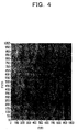
- Fig. 4 shows an image taken by an atomic force microscope (AFM) of the surface of the specimen after the heat treatment.
- AFM atomic force microscope
- Each of vertical stripes seen in the figure represents atomic surface step which corresponds to mono-molecular layer, and a region between the adjacent vertical stripes represents an identical atomic surface. From Figs. 3 and 4, it is seen that the top surface of the BaTiO 3 epitaxial thin film is flat and even on an atomic level.
- Fig. 5 shows images of a specimen comprising a SrTiO 3 substrate with a BaTiO 3 thin film epitaxially grown thereon, which is taken by a transmission electron diffraction microscope (TEM) in a direction perpendicular to the substrate surface, wherein Fig. 5(a) is an TEM image where spots therein correspond to lattice points and Fig. 5(b) is a figure obtained when the image of Fig. 5(a) is processed so as to visualize the continuity of lattice planes. From Fig. 5 it is seen that the substrate and the epitaxial thin film are almost continuous with each other in lattice planes and that the epitaxial thin film has a large number of discontinuities of lattice planes, namely dislocations therein.
- TEM transmission electron diffraction microscope
- Fig. 6 shows images of a specimen comprising a SrTiO 3 substrate having a BaTiO 3 thin film epitaxially grown on it and thereafter heat-treated, which is taken by the transmission electron diffraction microscope (TEM) in a direction perpendicular to the substrate surface, wherein Fig. 6(a) is an TEM image where spots therein correspond to lattice points and Fig. 6(b) is a figure obtained when the image of Fig. 6(a) is processed so as to visualize the continuity of lattice planes. In Fig. 6(a) it is seen that lattice points lie more orderly than in Fig. 5(a). From Fig.
- TEM transmission electron diffraction microscope
- dislocations exist only on the substrate surface, and not at all on epitaxial thin film. From these results it is seen that according to the method of the present invention the dislocations are anchored to the substrate surface and the top surface of the first epitaxial thin film is flattened to an atomic level.
- Fig. 7 is a chart illustrating a result of measurement by a four-axis X-ray diffraction apparatus of a distribution of lattice constants in the specimen mentioned above.
- the abscissa and ordinate axes are taken in the (300) and (003) directions of a reciprocal lattice space, respectively.
- the point A indicates the diffraction point of the BaTiO 3 epitaxial thin film where its diffraction intensity is the maximum
- the point B indicates the diffraction point of the SrTiO 3 crystal substrate where its diffraction intensity is the maximum.
- a substrate of SrTiO 3 crystal is adjusted to have a desired in-plane lattice constant.
- the SrTiO 3 crystal substrate was formed thereon at an epitaxial growth temperature of 650°C with an epitaxial thin film of BaTiO 3 as a first epitaxial thin film to a film thickness of 120 angstroms and then formed thereon at an epitaxial growth temperature of 650°C with an epitaxial thin film of Ba 0.5 Sr 0.5 TiO 3 as a second epitaxial thin film to a film thickness of 1800 angstroms, each by laser ablation in a vacuum chamber, and then in the same vacuum chamber was heat-treated to a temperature of about 1350°C for a period of about 1 hour by laser heating.
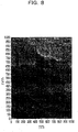
- Fig. 8 shows an image taken by the atomic force microscope (AFM) of the surface of the specimen after the heat treatment.
- vertical stripes represent atomic surface steps each of which corresponds to mono-molecular layer, and a region between the adjacent vertical stripes represents an identical atomic surface. From the Figure it is seen that the surface of Ba 0.5 Sr 0.5 TiO 3 epitaxial thin film is flat on an atomic level.
- the dislocations are anchored to the substrate surface, and the surface of the second epitaxial thin film is flattened to an atomic level.
- Fig. 9 is a figure illustrating a result of measurement by a four-axis X-ray diffraction apparatus of a distribution of lattice constants in the specimen mentioned above.
- the abscissa and ordinate axes are taken in the (300) and (003) directions of a reciprocal lattice space, respectively.
- the point C indicates the diffraction point of the Ba 0.5 Sr 0.5 TiO 3 epitaxial thin film as the second epitaxial thin film where its diffraction intensity is the maximum
- the point A indicates the diffraction point of the BaTiO 3 epitaxial thin film as the first epitaxial thin film where its diffraction intensity is the maximum.
- the in-plane lattice constant a of the BaTiO 3 epitaxial thin film as the first epitaxial thin film is 3.955 angstroms, which is a value as a lattice constant approximately equal to the in-plane lattice constant of Ba 0.5 Sr 0.5 TiO 3 mentioned above.
- Changing the ratio in thickness of the first to the second epitaxial growth films changes the in-plate lattice constants of the first and second epitaxial thin films. It is also possible to adjust the in-plane lattice constants by way of only the film thickness of the second epitaxial thin film.
- the heat-treatment temperature is shown to be lower than the melting points of materials used, some materials have constituent atoms diffusing in their solid state. With such materials, it is desirable that the heat treatment be effected at a temperature lower than their solid-state diffusion starting temperatures, namely their sintering temperatures.
- oxides having a perovskite-type crystallographic structure may be those having a different crystallographic structure, e. g., of a hexagonal system. It should also be apparent that the materials to which the present invention is applicable are not limited to oxides and may be any other materials.
- the present invention makes it possible to adjust the in-plane lattice constant of a substrate to have a desired value. Accordingly, the use of an in-plane lattice constant adjusted substrate of the present invention for a device utilizing an epitaxial thin film allows the device to be prepared having an extremely high quality.
- the present invention is extremely useful when used as a substrate, e. g., for high temperature oxide superconducting device.
Landscapes
- Chemical & Material Sciences (AREA)
- Engineering & Computer Science (AREA)
- Crystallography & Structural Chemistry (AREA)
- Materials Engineering (AREA)
- Metallurgy (AREA)
- Organic Chemistry (AREA)
- Physics & Mathematics (AREA)
- Thermal Sciences (AREA)
- Chemical Kinetics & Catalysis (AREA)
- General Chemical & Material Sciences (AREA)
- Inorganic Chemistry (AREA)
- Crystals, And After-Treatments Of Crystals (AREA)
Abstract
A method of adjusting the in-plane lattice constant of a
substrate and an in-plane lattice constant adjusted substrate are
provided. A crystalline substrate (1) made of SrTiO3 is formed at a
first preestablished temperature thereon with a first epitaxial thin
film (2) made of a first material, e. g., BaTiO3, and then on the first
epitaxial thin film (2) with a second epitaxial thin film (6) made of a
second material, e. g., BaxSr1-xTiO3 (where 0 < x < 1), that contains a
substance of the first material and another substance which together
therewith is capable of forming a solid solution in a preestablished
component ratio. Thereafter, the substrate is heat-treated at a second
preselected temperature. Heat treated at the second preestablished
temperature, the substrate has dislocations (4) introduced therein
and the second epitaxial thin film (6) has its lattice constant relaxed
to a value close to the lattice constant of bulk crystal of the second
material. Selecting the ratio of components x of the other substance in
the second material allows a desired in-plane lattice constant to be
realized.
Description
The present invention relates to a method of preparing an
in-plane lattice constant adjusted substrate, and an in-plane lattice
constant adjusted substrate, whereby a desired in-plane lattice
constant can be realized.
A thin film formed so that it is epitaxially grown on a
crystalline substrate has its properties influenced by its crystalline
perfectness. For example, in the preparation of an oxide
superconductor thin film such as of (Ba, Sr) CuO type which is
epitaxially grown on a substrate to form a laminated superconductor,
its superconductive transition temperature and superconductive
critical magnetic field are influenced by its crystalline perfectness
such as its crystal defect density and crystallographic orientation.
Also, an epitaxial BaTiO3 thin film used as a memory element in a
semiconductor integrated circuit has its capacity value largely varied
by its crystallographic orientation.
So far, in order to obtain a high quality thin film that is
satisfactory in crystalline perfectness, a substrate has been used
having an in-plane lattice constant that is close to the in-plane lattice
constant of the thin film. If there does not exist any substrate having
an in-plane lattice constant close to that of a thin film, a material is
chosen having an in-plane lattice constant intermediate between
those of the substrate and the thin film and is layered on the
substrate as a buffer layer on which the thin film may be grown.
It is, however, only rare that a substrate is available that
agrees in in-plane lattice constant with the thin film, and if such a
substrate is available, it often is extremely brittle or of high cost. In
the use of a buffer layer, too, it rarely is the case that a substrate is
available which is fully congruous in in-plane lattice constant.
Thus, in the past, since it has not been possible to grow a thin
film on a substrate that fully agrees or is congruent in in-plane lattice
constant therewith, it has been likely the case that a thin film has
dislocations introduced therein due to its lattice mismatch with the
substrate; hence a thin film results that is highly dense with crystal
defects, imperfect in crystalline orientation, and thus poor in quality
and properties, problems met by the prior art.
In view of the aforementioned problems in the prior art, the
present invention has for its object to provide a method of adjusting
the lattice constant of a substrate and to provide an in-plane lattice
constant adjusted substrate.
In order to achieve the object mentioned above, there is
provided in accordance with the present invention in a first form of
implementation thereof a method of preparing an in-plane lattice
constant adjusted substrate, characterized in that it comprises the
steps of: growing a first epitaxial thin film made of a first material on
a substrate at a first preestablished temperature; and heat-treating
at a second preestablished temperature the substrate having the first
epitaxial thin film grown thereon.
In the method of preparing an in-plane lattice constant
adjusted substrate in accordance with the present invention, the said
first preestablished temperature is a temperature that causes the said
first material to epitaxially grow on the said substrate.
Also, the said second preestablished temperature is a
temperature that is higher than the said first preestablished
temperature but lower than the lower of melting points of the said
substrate and the said first epitaxial thin film.
According to this method makeup, epitaxially growing a first
material on a substrate at a first preestablished temperature causes a
first epitaxial thin film having distortions due to its mismatch in
in-plane lattice constant with the substrate to epitaxially grow on the
substrate, and heat-treating the epitaxial thin film and the substrate
at a second preestablished temperature introduces dislocations into
the substrate surface and relaxes the in-plane lattice constant of the
first epitaxial thin film to a value close to the lattice constant of bulk
crystal of the first material. The dislocations are anchored to the
interface between the substrate and the first epitaxial thin film, the
top surface of the epitaxial thin film is flattened to an atomic level,
and they are left immobile when another material is epitaxially grown
on that surface.
In the present invention, the said substrate and the said first
epitaxial thin film are preferably made of oxides. It is also preferred
that the said substrate be made of SrTiO3 crystal and said first
epitaxial thin film be made of BaTiO3.
According to this method makeup, it is possible to adjust the
in-plane lattice constant of a single crystal substrate of SrTiO3 which
is of low cost and stout, to the lattice constant of BaTiO3. Also in an
application in which the in-plane lattice constant of BaTiO3 is
required, it can be used in place of a BaTiO3 which is brittle and of
high cost. For example, it becomes possible to manufacture at a low
cost BaTiO3 capacitors which are high in dielectric constant.
The present invention also provides in another form of
implementation thereof a method of preparing an in-plane lattice
constant adjusted substrate, characterized in that at a first
preestablished temperature, a first epitaxial thin film made of a first
material and having a first preselected film thickness is formed on a
substrate, and on the first epitaxial thin film there is formed a second
epitaxial thin film having a second preselected film thickness and
made of a second material that contains, at a predetermined ratio of
compositions, a substance of the first material and another substance
which is capable of forming a solid solution together with the said
substance; and they are heat-treated at a second preestablished
temperature.
In the method mentioned above, the said first preestablished
temperature is preferably a temperature that causes each of the said
first and second materials to epitaxially grow.
Also, the said second preestablished temperature is preferably
a temperature that is higher than the said first preestablished
temperature but lower than the lowest of melting points of the said
sub- strate, the said first epitaxial thin film and the said second
epitaxial thin film.
The said first preselected film thickness is preferably smaller
than the said second preselected film thickness.
Also, the said second epitaxial thin film may be formed to the
second preselected film thickness on the said substrate without using
the said first epitaxial thin film made of the first material and may
thereafter be heat-treated at the second preestablished temperature.
According to this method makeup, on the substrate there is
allowed to epitaxially grow a first epitaxial thin film having
distortions due to its mismatch in in-plane lattice constant with the
substrate, and on the first epitaxial thin film there is allowed to grow
epitaxially a second epitaxial thin film having distortions due to its
mismatch in in-plane lattice constant with the first epitaxial thin film,
and then heat-treating them at a second preestablished temperature
introduces dislocations into the substrate surface and into the
interface between the first and second epitaxial thin films and relaxes
the in-plane lattice constants of the first and second epitaxial thin
films to values close to the lattice constant of the bulk crystal of the
second material.
The dislocations are anchored to the interfaces between the
substrate and the first epitaxial thin film and between the latter and
the second epitaxial thin film, the top surface of the second epitaxial
thin film is flattened to an atomic level, and the dislocations are left
immobile when another material is caused to grow epitaxially on that
surface.
Suitably selecting the ratio of components of the other
substance in the said second material allows a desired in-plane lattice
constant determined by the selected ratio of components and hence a
substrate having such a desired in-plane lattice constant to be
obtained.
Further, the said substrate and the said first and second
epitaxial thin films are preferably made of oxides. It is preferred that
the said substrate be a SrTiO3 crystalline substrate, the said first
epitaxial thin film be made of BaTiO3 and the said second epitaxial
thin film be made of BaxSr1-xTiO3 where 0 < x < 1.
According to this method makeup, suitably selecting x allows
forming a substrate which agrees in in-plane lattice constant with a
thin film to be formed thereon. Thus, for example, such a substrate
can be used for forming a (Ba, Sr) CuO or like oxide superconductor
thin film thereon. Then, since a substrate can be formed which by
selecting x suitably is made substantially identical in in-plane lattice
constant to a superconductor layer to be formed thereon, it becomes
possible to obtain an oxide high-temperature superconductor film that
extremely excels in quality.
The present invention also provides an in-plane lattice
constant adjusted substrate, characterized in that it comprises a
crystalline substrate made of SrTiO3 and having a thin film of BaTiO3
formed thereon, wherein the BaTiO3 thin film has its top surface
flattened to an atomic level and is substantially equal in lattice
constant to BaTiO3 bulk crystal. A substrate so made up may be used,
in an application in which a BaTiO3 substrate is required, to replace
the same which is brittle and of high cost..
The present invention also provides a in-plane lattice constant
adjusted substrate, characterized in that it comprises a crystalline
substrate made of SrTiO3 and having a thin film of BaTiO3 formed
thereon and a thin film of BaxSr1-xTiO3 (where 0 < x < 1) formed on
the BaTiO3 thin film, wherein the BaxSr1-xTiO3 thin film has its top
surface flattened to an atomic level and has its lattice constant
adjustable to a desired length between the lattice constants of SrTiO3
and BaTiO3 bulk crystals by selecting x. A substrate so made up can
be used in forming a thin film thereon. Then, since a substrate can be
formed that agrees in in-plane lattice constant to a thin film to be
formed thereon, it is possible to form a thin film that extremely excels
in quality.
The present invention will better be understood from the
following detailed description and the drawings attached hereto
showing certain illustrative forms of implementation of the present
invention. In this connection, it should be noted that such forms of
implementation illustrated in the accompanying drawings hereof are
intended in no way to limit the present invention but to facilitate an
explanation and understanding thereof. In the drawings:
Hereinafter, the present invention will be described in detail
with reference to certain suitable forms of implementation thereof
illustrated in the drawing figures.
At the outset, mention is made of a first form of
implementation of the present invention.
Fig. 1 shows typical views illustrating the principles of
preparing an in-plane lattice constant adjusted substrate according to
a first form of implementation of the present invention wherein a
substrate 1 has a first epitaxial thin film 2 of a first material formed
thereon. Fig. 1(a) shows a state in crystal lattice of the substrate 1
and the first epitaxial thin film 2 typically in a cross section taken
perpendicular to a surface 3 of the substrate. The crystal lattices in
the substrate 1 and those in the first epitaxial thin film 2 are
typically represented by squares and rectangles, respectively, as
shown. Fig. 1(b) shows a state of the crystal lattice after the
heat-treatment of the substrate 1 formed with the first epitaxial
thin film 2 on it, which are shown typically in a cross section taken
perpendicular to the substrate surface 3. The crystal lattices in the
substrate 1 and those in the first epitaxial thin film 2 after the heat
treatment are again typically represented by squares and rectangles,
respectively, as shown.
The method of preparing an in-plane crystal lattice adjusting
substrate comprises a first step of supplying the substrate 1 at a first
preestablished temperature with a first material over it to grow a
first epitaxial thin film 2 composed of the first material on the
substrate 1. The first preestablished temperature may be any low or
high temperature if it allows the epitaxial growth of the first
epitaxial thin film 2. Here, any epitaxial growth process, such as
MOCVD, CVD or laser ablation, may be adopted in epitaxially
growing the first material on the substrate 1.
As shown in Fig. 1(a), the first epitaxial thin film 2 is formed
on the substrate so that the lattice planes in the first epitaxial thin
film 2 are substantially continuous with those in the substrate 1 and
that the in-plane lattice constant a1 in the first epitaxial thin film 2 is
substantially equal to the in-plane lattice constant as in the substrate
1. Also the lattice constant of the first epitaxial thin film 2 in a
direction perpendicular to the substrate surface 3 is different from
the lattice constant of the first material in its bulk state. Therefore
the first epitaxial thin film 2 is grown on the substrate 1 in a state
that it has distortions due to its mismatch in in-plane lattice constant
with the substrate 1.
Then, the substrate 1 on which the first epitaxial thin film 2
has been grown is heat-treated at a second preestablished
temperature, which is a temperature higher than the first
preestablished temperature, but lower than the lower of the melting
points of the substrate 1 and the first epitaxial thin film 2.
With this heat treatment, as shown in Fig. 1(b), a dislocation
4 is introduced into the substrate surface 3 while the distortions in
the first epitaxial thin film 2 is relieved with the result that the
in-plane lattice constant a1 in the first epitaxial thin film 2 becomes
substantially equal to the lattice constant of the first material in its
bulk state. Further, its lattice constant in a direction perpendicular to
the substrate surface 3 also relaxes and becomes substantially equal
to the lattice constant in its bulk state. The dislocations 4 are
anchored to the substrate surface 3 while the first epitaxial thin film
2 has its top surface 5 flattened to an atomic level, thereby permitting
another material to grow epitaxially thereon while leaving the
dislocations 4 anchored immobile.
Mention is next made of a second form of implementation of
the present invention.
Fig. 2 shows typical views illustrating the principles of
preparing an in-plane lattice constant adjusted substrate according to
a second form of implementation of the present invention, wherein a
substrate 1 has a first epitaxial thin film 2 of a first material formed
thereon by a preselected film thickness, which in turn has a second
epitaxial thin film 6 of a second material formed thereon by a
predetermined thickness. Fig. 2(a) shows a state in crystal lattice of
the substrate 1, the first epitaxial thin film 2 and the second epitaxial
thin film 6 typically in a cross section taken perpendicular to a
surface 3 of the substrate 1. The crystal lattices of the substrate 1
and the crystal lattices of the first and second epitaxial thin films 2
and 6 are typically represented by squares and rectangles,
respectively, as shown.
Fig. 2(b) shows a state in crystal lattice of the substrate 1 and
the first and second epitaxial thin films 2 and 6 which are formed as
mentioned above and then are heat-treated at a second preestablished
temperature. The state is shown typically in a cross section taken
perpendicular to the substrate surface 3. The crystal lattices of the
substrate 1 and those of the first and second epitaxial thin films 2
and 6 are again typically represented by squares and rectangles,
respectively, as shown.
The method of a preparing an in-plane lattice constant
adjusted substrate of the present invention in this form of
implementation comprises a first step of supplying a substrate 1 at a
first preestablished temperature with a first material over it to grow
a first epitaxial thin film 2 of a first predetermined film thickness on
the substrate 1 and subsequently supplying a second material to grow
a second epitaxial thin film 6 of a second predetermined film
thickness thereon. Here, the first predetermined film thickness is
made sufficiently thinner than the second predetermined film
thickness. The second material should contain a substance of the first
material and another substance that is capable of forming a solid
solution together with that substance, at a preselected ratio of
components. The first preestablished temperature may be any low or
high temperature if it allows the epitaxial growth of the thin film.
Here, any epitaxial growth process, such as MOCVD, CVD or laser
ablation, may be adopted in epitaxially growing the first and second
materials on the substrate 1.
As shown in Fig. 2(a), the first and second epitaxial thin films
are formed on the substrate so that the lattice planes in the first and
second epitaxial thin films 2 and 6 are substantially continuous
mutually and with those in the substrate 1 and that the in-plane
lattice constants a1 and a2 in the first and the second epitaxial thin
films 2 and 6 are substantially equal to the in-plane lattice constant
as in the substrate 1. Therefore, the first and second epitaxial thin
films 2 and 6 are epitaxially grown on the substrate 1 in a state that
they have distortions due to their mismatch in in-plane lattice
constant.
Then, the substrate 1 on which the epitaxial thin films 2 and
6 have been grown is heat-treated at a second preestablished
temperature which is a temperature higher than the first
preestablished temperature, but lower than the lowest of the melting
points of the substrate 1 and the first and second epitaxial thin films
2 and 6. With this heat treatment, as shown in Fig. 2(b), dislocations
4 are introduced into both the substrate surface 3 and the interface 7
between the first and second epitaxial thin films 2 and 6 or the
substrate surface 3 alone to relax the in-plane lattice constants in the
first and second epitaxial thin films 2 and 6. Further, with the first
predetermined film thickness made sufficiently thinner than the
second predetermined film thickness, the in-plane lattice constants of
the first and second epitaxial thin films 2 and 6 relax to a value close
to the lattice constant of the second material in its bulk crystal state.
The in-plane lattice constant a2 changes according to the component
ratio of the second material, namely the ratio in amount of the
substance of the first material to the other substance forming the
solid solution together therewith. Their lattice constants in a
direction perpendicular to the substrate surface 3 also relax. The
dislocations 4 are anchored to both the substrate surface 3 and the
interface 7 or to the substrate surface 3 alone while the second
epitaxial thin film 6 has its top surface 8 flattened to an atomic level,
thereby permitting another material to grow epitaxially thereon while
leaving the dislocations anchored immobile.
The present invention thus enables the in-plane lattice
constant of a substrate to be adjusted to a desired value, thereby
permitting a device preparation process using an epitaxial thin film to
be furnished with a substrate having an optimum in-plate lattice
constant.
Mention is next made of a specific example of the first form of
implementation of the present invention.
A specific example is here shown in which a substrate of
SrTiO3 crystal is adjusted to have a in-plane lattice constant of
BaTiO3. As a specimen the SrTiO3 crystal substrate was formed
thereon at an epitaxial growth temperature of 650 °C with an
epitaxial thin film of BaTiO3 as the first epitaxial thin film to a film
thickness of 120 angstroms by laser ablation in a vacuum chamber,
and then in the same vacuum chamber was heat-treated to a
temperature of about 1350°C for a period of about 1 hour by laser
heating.
Fig. 3 shows images by a scanning tunnel electron microscope
of a substrate surface, an epitaxial thin film surface before the heat
treatment and an epitaxial thin film surface after the heat treatment.
The BaTiO3 epitaxial thin film grown on the SrTiO3 crystal substrate
whose surface is flat on an atomic level as shown in Fig. 3(a) is seen
to have a top surface that is keenly irregular or uneven as shown in
Fig. 3(b). With the heat treatment applied to the substrate, a film top
surface that is flat or even on an atomic level as shown in Fig. 3(c)
has obtained. Each of vertical stripes in Figs. 3(a) and 3(b) represents
an atomic surface step which corresponds to mono-molecular layer,
and a region between the adjacent vertical stripes represents an
identical atomic surface. Fig. 4 shows an image taken by an atomic
force microscope (AFM) of the surface of the specimen after the heat
treatment. Each of vertical stripes seen in the figure represents
atomic surface step which corresponds to mono-molecular layer, and a
region between the adjacent vertical stripes represents an identical
atomic surface. From Figs. 3 and 4, it is seen that the top surface of
the BaTiO3 epitaxial thin film is flat and even on an atomic level.
Fig. 5 shows images of a specimen comprising a SrTiO3
substrate with a BaTiO3 thin film epitaxially grown thereon, which is
taken by a transmission electron diffraction microscope (TEM) in a
direction perpendicular to the substrate surface, wherein Fig. 5(a) is
an TEM image where spots therein correspond to lattice points and
Fig. 5(b) is a figure obtained when the image of Fig. 5(a) is processed
so as to visualize the continuity of lattice planes. From Fig. 5 it is
seen that the substrate and the epitaxial thin film are almost
continuous with each other in lattice planes and that the epitaxial
thin film has a large number of discontinuities of lattice planes,
namely dislocations therein.
Fig. 6 shows images of a specimen comprising a SrTiO3
substrate having a BaTiO3 thin film epitaxially grown on it and
thereafter heat-treated, which is taken by the transmission electron
diffraction microscope (TEM) in a direction perpendicular to the
substrate surface, wherein Fig. 6(a) is an TEM image where spots
therein correspond to lattice points and Fig. 6(b) is a figure obtained
when the image of Fig. 6(a) is processed so as to visualize the
continuity of lattice planes. In Fig. 6(a) it is seen that lattice points
lie more orderly than in Fig. 5(a). From Fig. 6(b) it is seen that
dislocations exist only on the substrate surface, and not at all on
epitaxial thin film. From these results it is seen that according to the
method of the present invention the dislocations are anchored to the
substrate surface and the top surface of the first epitaxial thin film is
flattened to an atomic level.
Fig. 7 is a chart illustrating a result of measurement by a
four-axis X-ray diffraction apparatus of a distribution of lattice
constants in the specimen mentioned above. In the chart, the abscissa
and ordinate axes are taken in the (300) and (003) directions of a
reciprocal lattice space, respectively. In the chart, the point A
indicates the diffraction point of the BaTiO3 epitaxial thin film where
its diffraction intensity is the maximum, and the point B indicates the
diffraction point of the SrTiO3 crystal substrate where its diffraction
intensity is the maximum. From the coordinate of point A it is seen
that the in-plane lattice constant a of the BaTiO3 epitaxial thin film
is 3.990 angstroms, which is approximately equal to the lattice
constant of BaTiO3 bulk crystal (a = 4.000 angstroms). It is seen that
according to the method of the present invention, the in-plane lattice
constant of the first epitaxial thin film is relaxed to the lattice
constant of its bulk crystal.
Mention is next made of a specific example of the second form
of implementation of the present invention. Here, a specific example
is shown in which a substrate of SrTiO3 crystal is adjusted to have a
desired in-plane lattice constant. As a specimen the SrTiO3 crystal
substrate was formed thereon at an epitaxial growth temperature of
650°C with an epitaxial thin film of BaTiO3 as a first epitaxial thin
film to a film thickness of 120 angstroms and then formed thereon at
an epitaxial growth temperature of 650°C with an epitaxial thin film of
Ba0.5Sr0.5TiO3 as a second epitaxial thin film to a film thickness of
1800 angstroms, each by laser ablation in a vacuum chamber, and
then in the same vacuum chamber was heat-treated to a temperature
of about 1350°C for a period of about 1 hour by laser heating.
Fig. 8 shows an image taken by the atomic force microscope
(AFM) of the surface of the specimen after the heat treatment. In the
Figure, vertical stripes represent atomic surface steps each of which
corresponds to mono-molecular layer, and a region between the
adjacent vertical stripes represents an identical atomic surface. From
the Figure it is seen that the surface of Ba0.5Sr0.5TiO3 epitaxial thin
film is flat on an atomic level. Thus, according to the method of the
present invention, the dislocations are anchored to the substrate
surface, and the surface of the second epitaxial thin film is flattened
to an atomic level.
Fig. 9 is a figure illustrating a result of measurement by a
four-axis X-ray diffraction apparatus of a distribution of lattice
constants in the specimen mentioned above. In the figure, the
abscissa and ordinate axes are taken in the (300) and (003) directions
of a reciprocal lattice space, respectively. In the figure, the point C
indicates the diffraction point of the Ba0.5Sr0.5TiO3 epitaxial thin film
as the second epitaxial thin film where its diffraction intensity is the
maximum, and the point A indicates the diffraction point of the
BaTiO3 epitaxial thin film as the first epitaxial thin film where its
diffraction intensity is the maximum. From the coordinate of point C
it is seen that the in-plane lattice constant a of the Ba0.5Sr0.5TiO3
epitaxial thin film is 3.952 angstroms, which is a value as a lattice
constant intermediate between the lattice constant of SrTiO3 bulk
crystal of the substrate (a = 3.905 angstroms) and the lattice constant
of BaTiO3 bulk crystal (a = 4.000 angstroms). From the coordinate of
point A it is seen that the in-plane lattice constant a of the BaTiO3
epitaxial thin film as the first epitaxial thin film is 3.955 angstroms,
which is a value as a lattice constant approximately equal to the
in-plane lattice constant of Ba0.5Sr0.5TiO3 mentioned above. The fact
that the film thickness of Ba0.5Sr0.5TiO3 being 1800 angstroms is
much thicker than the film thickness of BaTiO3 being 120 angstroms
allows the in-plane lattice constant of the BaTiO3 epitaxial thin film
as the first epitaxial thin film to take a value close to the in-plane
lattice constant of Ba0.5Sr0.5TiO3.
Changing the ratio in thickness of the first to the second
epitaxial growth films changes the in-plate lattice constants of the
first and second epitaxial thin films. It is also possible to adjust the
in-plane lattice constants by way of only the film thickness of the
second epitaxial thin film.
While in this specific example the ratio x of components is
made 0.5, it will be apparent that suitably changing the ratio x allows
realizing a desired in-plane lattice constant intermediate between the
lattice of substrate SrTiO3 (a = 3.952 angstroms) and the lattice
constant of bulk BaTiO3 (a = 4.000). According to the method of the
present invention it is thus seen that suitably selecting the ratio of
component x allows adjusting the in-plane lattice constant of a second
epitaxial thin film to have a desired value.
While in the foregoing description the heat-treatment
temperature is shown to be lower than the melting points of materials
used, some materials have constituent atoms diffusing in their solid
state. With such materials, it is desirable that the heat treatment be
effected at a temperature lower than their solid-state diffusion
starting temperatures, namely their sintering temperatures.
Also, while in the foregoing specific examples, an example is
taken of oxides having a perovskite-type crystallographic structure, it
should be apparent that the oxides may be those having a different
crystallographic structure, e. g., of a hexagonal system. It should also
be apparent that the materials to which the present invention is
applicable are not limited to oxides and may be any other materials.
As will be appreciated from the foregoing description, the
present invention makes it possible to adjust the in-plane lattice
constant of a substrate to have a desired value. Accordingly, the use
of an in-plane lattice constant adjusted substrate of the present
invention for a device utilizing an epitaxial thin film allows the device
to be prepared having an extremely high quality. The present
invention is extremely useful when used as a substrate, e. g., for high
temperature oxide superconducting device.
Claims (14)
- A method of preparing an in-plane lattice constant adjusted substrate, characterized in that it comprises the steps of:growing a first epitaxial thin film made of a first material on a substrate at a first preestablished temperature; andheat-treating at a second preestablished temperature the substrate having the first epitaxial thin film grown thereon.
- A method of preparing an in-plane lattice constant adjusted substrate as set forth in claim 1, characterized in that said first preestablished temperature is a temperature that causes said first material to epitaxially grow on said substrate.
- A method of preparing an in-plane lattice constant adjusted substrate as set forth in claim 1, characterized in that said second preestablished temperature is a temperature that is higher than said first preestablished temperature but lower than the lower of melting points of said substrate and said first epitaxial thin film.
- A method of preparing an in-plane lattice constant ajusted substrate as set forth in claim 1, characterized in that said substrate and said first epitaxial thin film are made of oxides.
- A method of preparing an in-plane lattice constant adjusted substrate as set forth in claim 1, characterized in that said substrate is a SrTiO3 crystalline substrate and said first epitaxial thin film is made of BaTiO3.
- A method of preparing an in-plane lattice constant ajusted substrate, characterized in that it comprises the steps of:forming, at a first preestablished temperature, a first epitaxial thin film made of a first material and having a first preselected film thickness on a substrate, and then on the first epitaxial thin film a second epitaxial thin film having a second preselected film thickness and made of a second material that contains, at a predetermined ratio of compositions, a substance of the first material and another substance which is capable of forming a solid solution together with said substance; and thereafterheat-treating them at a second preestablished temperature.
- A method of preparing an in-plane lattice constant adjusted substrate as set forth in claim 6, characterized in that said second epitaxial thin film is formed to the second preselected film thickness on said substrate without using said first epitaxial thin film made of the first material and is heat-treated at the second preestablished temperature.
- A method of preparing an in-plane lattice constant adjusted substrate as set forth in claim 6, characterized in that said first preestablished temperature is a temperature that causes each of said first and second materials to epitaxially grow.
- A method of preparing an in-plane lattice constant adjusted substrate as set forth in claim 6, characterized in that said second preestablished temperature is a temperature that is higher than said first preestablished temperature but lower than the lowest of melting points of said substrate, said first epitaxial thin film and said second epitaxial thin film.
- A method of preparing an in-plane lattice constant adjusted substrate as set forth in claim 6, characterized in that said first preselected film thickness is smaller than said second preselected film thickness.
- A method of preparing an in-plane lattice constant adjusted substrate as set forth in claim 6, characterized in that said substrate and said first and second epitaxial thin films are made of oxides.
- A method of preparing an in-plane lattice constant adjusted substrate as set forth in claim 6, characterized in that said substrate is a SrTiO3 crystalline substrate, said first epitaxial thin film is made of BaTiO3 and said second epitaxial thin film is made of BaRSr1-xTiO3 where 0 < x < 1.
- An in-plane lattice constant adjusted substrate, characterized in that it comprises a SrTiO3 crystalline substrate and having a thin film of BaTiO3 formed thereon, wherein the BaTiO3 thin film has its top surface flattened to an atomic level and is substantially equal in lattice constant to BaTiO3 bulk crystal.
- An in-plane lattice constant adjusted substrate, characterized in that it comprises a SrTiO3 crystalline substrate and having a thin film of BaTiO3 formed thereon and a thin film of BaxSr1-xTiO3 (where 0 < x < 1) formed on the BaTiO3 thin film, wherein the BaxSr1-xTiO3 thin film has its top surface flattened to an atomic level and has its in-plate lattice constant adjustable to a desired length between the lattice constants of SrTiO3 and BaTiO3 bulk crystals by selecting x.
Applications Claiming Priority (3)
| Application Number | Priority Date | Filing Date | Title |
|---|---|---|---|
| JP2001250842A JP3762978B2 (en) | 2001-08-21 | 2001-08-21 | Method for producing in-plane lattice constant adjusting substrate and in-plane lattice constant adjusting substrate |
| JP2001250842 | 2001-08-21 | ||
| PCT/JP2002/008409 WO2003016600A1 (en) | 2001-08-21 | 2002-08-21 | Method for manufacturing in-plane lattice constant adjusting substrate and in-plane lattice constant adjusting substrate |
Publications (2)
| Publication Number | Publication Date |
|---|---|
| EP1437427A1 true EP1437427A1 (en) | 2004-07-14 |
| EP1437427A4 EP1437427A4 (en) | 2008-05-28 |
Family
ID=19079579
Family Applications (1)
| Application Number | Title | Priority Date | Filing Date |
|---|---|---|---|
| EP02762816A Ceased EP1437427A4 (en) | 2001-08-21 | 2002-08-21 | METHOD FOR MANUFACTURING A SUBSTRATE ADJUSTING THE CRYSTALLINE NETWORK CONSTANT IN THE PLAN AND SUBSTRATE THUS OBTAINED |
Country Status (4)
| Country | Link |
|---|---|
| US (1) | US7150788B2 (en) |
| EP (1) | EP1437427A4 (en) |
| JP (1) | JP3762978B2 (en) |
| WO (1) | WO2003016600A1 (en) |
Cited By (1)
| Publication number | Priority date | Publication date | Assignee | Title |
|---|---|---|---|---|
| DE102013202851A1 (en) | 2013-02-21 | 2014-08-21 | Leibniz-Institut Für Festkörper- Und Werkstoffforschung Dresden E.V. | Layer system used for the determination from properties of the material of functional layers, comprises primary layer having specific crystal orientation, secondary layer with continuous change in composition |
Families Citing this family (2)
| Publication number | Priority date | Publication date | Assignee | Title |
|---|---|---|---|---|
| KR102776257B1 (en) * | 2020-11-18 | 2025-03-07 | 삼성전기주식회사 | Multilayered electronic component |
| WO2026028689A1 (en) * | 2024-08-02 | 2026-02-05 | 株式会社村田製作所 | Joined body, optical modulator, and method for manufacturing joined body |
Family Cites Families (12)
| Publication number | Priority date | Publication date | Assignee | Title |
|---|---|---|---|---|
| JPH02258700A (en) | 1989-03-30 | 1990-10-19 | Res Inst For Prod Dev | Ferroelectric thin film and production thereof |
| US5198269A (en) * | 1989-04-24 | 1993-03-30 | Battelle Memorial Institute | Process for making sol-gel deposited ferroelectric thin films insensitive to their substrates |
| US5650362A (en) * | 1993-11-04 | 1997-07-22 | Fuji Xerox Co. | Oriented conductive film and process for preparing the same |
| JP3989027B2 (en) | 1994-07-12 | 2007-10-10 | テキサス インスツルメンツ インコーポレイテツド | Capacitor and manufacturing method thereof |
| JPH101391A (en) * | 1996-06-18 | 1998-01-06 | Ngk Insulators Ltd | Manufacturing method of ferroelectric optical single crystal substrate product |
| JPH10152398A (en) | 1996-11-18 | 1998-06-09 | Nippon Telegr & Teleph Corp <Ntt> | Method of forming ferroelectric thin film |
| JP3472087B2 (en) * | 1997-06-30 | 2003-12-02 | Tdk株式会社 | Film structure, electronic device, recording medium, and method for producing oxide conductive thin film |
| US5943111A (en) * | 1998-06-09 | 1999-08-24 | Symetrix Corporation | Layered superlattice ferroelectric liquid crystal display |
| JP2000066050A (en) * | 1998-08-19 | 2000-03-03 | Ngk Insulators Ltd | Method of manufacturing optical waveguide component and optical waveguide component |
| US6255121B1 (en) * | 1999-02-26 | 2001-07-03 | Symetrix Corporation | Method for fabricating ferroelectric field effect transistor having an interface insulator layer formed by a liquid precursor |
| US6610548B1 (en) * | 1999-03-26 | 2003-08-26 | Sony Corporation | Crystal growth method of oxide, cerium oxide, promethium oxide, multi-layered structure of oxides, manufacturing method of field effect transistor, manufacturing method of ferroelectric non-volatile memory and ferroelectric non-volatile memory |
| US6198225B1 (en) * | 1999-06-07 | 2001-03-06 | Symetrix Corporation | Ferroelectric flat panel displays |
-
2001
- 2001-08-21 JP JP2001250842A patent/JP3762978B2/en not_active Expired - Fee Related
-
2002
- 2002-08-21 WO PCT/JP2002/008409 patent/WO2003016600A1/en not_active Ceased
- 2002-08-21 US US10/486,571 patent/US7150788B2/en not_active Expired - Fee Related
- 2002-08-21 EP EP02762816A patent/EP1437427A4/en not_active Ceased
Cited By (1)
| Publication number | Priority date | Publication date | Assignee | Title |
|---|---|---|---|---|
| DE102013202851A1 (en) | 2013-02-21 | 2014-08-21 | Leibniz-Institut Für Festkörper- Und Werkstoffforschung Dresden E.V. | Layer system used for the determination from properties of the material of functional layers, comprises primary layer having specific crystal orientation, secondary layer with continuous change in composition |
Also Published As
| Publication number | Publication date |
|---|---|
| US7150788B2 (en) | 2006-12-19 |
| JP2003055100A (en) | 2003-02-26 |
| JP3762978B2 (en) | 2006-04-05 |
| EP1437427A4 (en) | 2008-05-28 |
| WO2003016600A1 (en) | 2003-02-27 |
| US20040197936A1 (en) | 2004-10-07 |
Similar Documents
| Publication | Publication Date | Title |
|---|---|---|
| Eom et al. | Single-Crystal Epitaxial Thin Films of the Isotropic Metallic Oxides Sr1–x Ca x RuO3 (0≤×≤ 1) | |
| US5426092A (en) | Continuous or semi-continuous laser ablation method for depositing fluorinated superconducting thin film having basal plane alignment of the unit cells deposited on non-lattice-matched substrates | |
| DE69430550T2 (en) | Improvements in heteroepitaxy through large surface levels | |
| Fork et al. | Effects of homoepitaxial surfaces and interface compounds on the in-plane epitaxy of YBCO films on yttria-stabilized zirconia | |
| US6261704B1 (en) | MgO buffer layers on rolled nickel or copper as superconductor substrates | |
| EP0472159B1 (en) | Method of fabricating a YBaCuO superconducting epitaxial-like thin film | |
| Kavanagh et al. | High-temperature epitaxy of PtSi/Si (0 0 1) | |
| Han et al. | Formation of Cu‐rich particles on the surface of YBa2Cu3O7− x thin film grown by in situ off‐axis sputtering | |
| US5508255A (en) | Epitaxial thallium high temperature superconducting films formed via a nucleation layer | |
| US7150788B2 (en) | Method for manufacturing in-plane lattice constant adjusting substrate and in-plane lattice constant adjusting substrate | |
| Tiwari et al. | Synthesis of epitaxial Pt on (100) Si using TiN buffer layer by pulsed laser deposition | |
| CN1312332C (en) | Oxide high-temperature superconductor and its preparation method | |
| EP2131408B1 (en) | Process for the preparation of a shaped substrate for a coated conductor and coated conductor using said substrate | |
| Lee et al. | Microstructure of epitaxially oriented superconducting YBa2Cu3O7− x films grown on (100) MgO by metalorganic decomposition | |
| JP2653003B2 (en) | Oxide superconducting thin film synthesis method | |
| Zandbergen et al. | HREM characterisation of interfaces in YBa2Cu3O7− δ/CeO2/R-Al2O3 structures | |
| US6191073B1 (en) | Series of layers and component containing such | |
| Aleksiyko et al. | Common features of gallium perovskites | |
| KR100338250B1 (en) | Method for improving the surface smoothness of YBa2Cu3O7-δhigh-temperature superconductor films grown on CeO2-buffered r-cut sapphire substrates | |
| Yang et al. | Monoclinic phase transition and twinning in Bi 2 Sr 2 CaCu 2 O y single crystals | |
| KR100781202B1 (en) | Method of solid-phase flux epitaxy growth | |
| Streiffer et al. | Morphology and Defect Structure of Sputtered High-Quality In-Situ YBa2Cu3O7− δ Films | |
| Mancini et al. | MgO/TiN buffer layer structures for coated conductor development on Cu-based substrates | |
| JP4809700B2 (en) | YBCO high temperature superconductor film-forming substrate and YBCO high temperature superconductor film production method | |
| Verbist et al. | Microstructure of Josephson junctions in relation to their properties |
Legal Events
| Date | Code | Title | Description |
|---|---|---|---|
| PUAI | Public reference made under article 153(3) epc to a published international application that has entered the european phase |
Free format text: ORIGINAL CODE: 0009012 |
|
| 17P | Request for examination filed |
Effective date: 20040308 |
|
| AK | Designated contracting states |
Kind code of ref document: A1 Designated state(s): AT BE BG CH CY CZ DE DK EE ES FI FR GB GR IE IT LI LU MC NL PT SE SK TR |
|
| A4 | Supplementary search report drawn up and despatched |
Effective date: 20080429 |
|
| 17Q | First examination report despatched |
Effective date: 20091022 |
|
| STAA | Information on the status of an ep patent application or granted ep patent |
Free format text: STATUS: THE APPLICATION HAS BEEN REFUSED |
|
| 18R | Application refused |
Effective date: 20101213 |