EP1435574A2 - A structure and method for detecting errors in a multilevel memory device with improved programming granularity - Google Patents
A structure and method for detecting errors in a multilevel memory device with improved programming granularity Download PDFInfo
- Publication number
- EP1435574A2 EP1435574A2 EP03104709A EP03104709A EP1435574A2 EP 1435574 A2 EP1435574 A2 EP 1435574A2 EP 03104709 A EP03104709 A EP 03104709A EP 03104709 A EP03104709 A EP 03104709A EP 1435574 A2 EP1435574 A2 EP 1435574A2
- Authority
- EP
- European Patent Office
- Prior art keywords
- subset
- digits
- sequence
- bits
- words
- Prior art date
- Legal status (The legal status is an assumption and is not a legal conclusion. Google has not performed a legal analysis and makes no representation as to the accuracy of the status listed.)
- Granted
Links
Images


Classifications
-
- G—PHYSICS
- G06—COMPUTING OR CALCULATING; COUNTING
- G06F—ELECTRIC DIGITAL DATA PROCESSING
- G06F11/00—Error detection; Error correction; Monitoring
- G06F11/07—Responding to the occurrence of a fault, e.g. fault tolerance
- G06F11/08—Error detection or correction by redundancy in data representation, e.g. by using checking codes
- G06F11/10—Adding special bits or symbols to the coded information, e.g. parity check, casting out 9's or 11's
- G06F11/1008—Adding special bits or symbols to the coded information, e.g. parity check, casting out 9's or 11's in individual solid state devices
- G06F11/1072—Adding special bits or symbols to the coded information, e.g. parity check, casting out 9's or 11's in individual solid state devices in multilevel memories
-
- G—PHYSICS
- G11—INFORMATION STORAGE
- G11C—STATIC STORES
- G11C11/00—Digital stores characterised by the use of particular electric or magnetic storage elements; Storage elements therefor
- G11C11/56—Digital stores characterised by the use of particular electric or magnetic storage elements; Storage elements therefor using storage elements with more than two stable states represented by steps, e.g. of voltage, current, phase, frequency
- G11C11/5621—Digital stores characterised by the use of particular electric or magnetic storage elements; Storage elements therefor using storage elements with more than two stable states represented by steps, e.g. of voltage, current, phase, frequency using charge storage in a floating gate
-
- G—PHYSICS
- G11—INFORMATION STORAGE
- G11C—STATIC STORES
- G11C29/00—Checking stores for correct operation ; Subsequent repair; Testing stores during standby or offline operation
- G11C29/04—Detection or location of defective memory elements, e.g. cell constructio details, timing of test signals
- G11C2029/0409—Online test
-
- G—PHYSICS
- G11—INFORMATION STORAGE
- G11C—STATIC STORES
- G11C29/00—Checking stores for correct operation ; Subsequent repair; Testing stores during standby or offline operation
Definitions
- the present invention relates to an error correction structure and a corresponding method for a multilevel memory device.
- Multilevel memory devices such as, for example, flash E 2 PROMs
- flash E 2 PROMs Flash E 2 PROMs
- each cell can take a number of states higher than two (each state being associated with a corresponding logic value).
- the multilevel memory devices provide high information transfer speeds in burst mode. Consequently, the multilevel memory devices are well suited to a number of end-product applications, such as solid state mass memories, cellular telephones, digital still cameras, multimedia devices, and the like.
- a still open question relating to the multilevel memory devices is their reliability.
- the multilevel memory devices are considered more sensitive to data retention problems and to noise than equivalent traditional memory devices (at two levels). Consequently, many producers equip the multilevel memory devices with error detection structures.
- ECC Error Correction Codes
- the error correction codes add redundant control information to each predefined set of logic values (for example, consisting of a page formed by four words each one of 16 bits). This control information is used for detecting and correcting (if possible) any errors in the page. This allows tolerating a drift of the cells in the multilevel memory device without impairing its operation.
- the error detection structures known in the art involve a considerable waste of space for storing the control information associated with the various pages.
- the logic networks commonly used for calculating the control information require a high number of levels; such levels introduce corresponding propagation delays of the signals, thereby slowing down the operation of the whole multilevel memory device.
- the error detection structures impose some constraints to the operation of the multilevel memory device. Particularly, once a page with the respective control information has been written onto the multilevel memory device, it is generally impossible to modify its content any longer (without a complete erasing and re-writing of the updated page with the new control information). In the same way, this requires the reading of a whole page (for verifying its correctness), before the content thereof can be used. In other words, the size of the page defines the granularity of the multilevel memory device.
- the present invention provides an error detection structure for a multilevel memory device including a plurality of memory cells each one being programmable at more than two levels ordered in a sequence, each level representing a logic value consisting of a plurality of digits, wherein the structure includes means for detecting errors in the values of a selected block of memory cells; the structure further includes means for partitioning the digits of each memory cell of the block into a first subset and a second subset, the digits of the first subset being unchanged in the values of a first and a second ending range in the sequence, the means for detecting errors only operating on the digits of the second subset of the block.
- the present invention proposes a multilevel memory device including this structure; a corresponding error detection method for a multilevel memory device is also encompassed.
- a nonvolatile memory device 100 for example, consisting of a flash E 2 PROM, is illustrated.
- the flash memory 100 is integrated on a chip of semiconductor material, and includes a matrix 105 of memory cells (for example, having a so-called NOR architecture).
- Each memory cell consists of a floating gate MOS transistor.
- the memory cell in a non-programmed (or erased) condition exhibits a low threshold voltage.
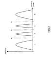
- the memory cell is programmed by injecting electric charge into its floating gate; the memory cell can be programmed at multiple levels, each one associated with a corresponding range of its threshold voltage. Each level represents a different logic value; for example, the flash memory 100 supports 4 levels, so that each memory cell stores a logic value consisting of 2 bits of information (11, 10, 01 and 00 for increasing threshold voltages).
- the flash memory 100 uses an error correction code, in which control information is associated with the information actually stored in the memory cells.
- a row decoder 110r is used for selecting one row of the matrix 105; similarly, a column decoder 110c is used for selecting one or more columns of the matrix 105.
- the memory cells of the matrix 105 are selected (by the decoders 110r and 110c) in response to an address ADR.
- the information stored in the matrix 105 is logically organized into words, each one consisting of 16 bits; the words are in turn grouped into pages of 4 consecutive words.
- a unit (R/W) 115 is used for reading and writing the memory cells selected by the decoders 110r and 110c.
- the above-described structure allows selecting (in reading and/or programming mode) the memory cells associated with a page, a word or a single bit.
- the values to be written onto the matrix 105 or to be read from the matrix 105 are latched into an input/output buffer 120. Particularly, this allows executing a reading in burst mode, in which a sequence of bits is provided in succession (from the input/output buffer 120) at each clock signal.
- a control logic 125 (for example, consisting of a state machine) manages the operation of the flash memory 100. For this purpose, the control logic 125 outputs a sequence of control signals (denoted as a whole with Sc).
- the concepts of the present invention are also applicable when the flash memory has a different architecture, when the memory cells are implemented by equivalent devices, or when the memory cells are programmable at another number of levels (also different from a power of 2). Similar considerations apply if each page and/or word has a different size, if another memory device is used (for example, an EPROM), and the like.
- the error correction code allows detecting and automatically correcting each error of a single bit in any position of a predetermined block of information. Such an error is caused by the drift of one of the memory cells used for storing the block of information. In this situation, the threshold voltage of the memory cell shifts from a correct level to a level adjacent thereto; particularly, if the floating gate of the memory cell has lost its electric charge, the threshold voltage will decrease (with a consequent increase of a bit of the stored logic value), while if the memory cell has incremented its electric charge the threshold voltage will increase (with a consequent decrease of a bit of the stored logic value). In order to detect and correct such an error in a block of information consisting of m bits, it is necessary to provide a block of control information consisting of k bits, where: k ⁇ log 2 m+1
- the control information in calculated on a halved number of bits, thereby reducing its memory occupation.
- the concepts of the present invention are also applicable when the error correction code is able to correct a different number of errors, when another control code is used (for example, only able to detect the errors but not to correct them), and the like.
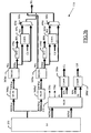
- the unit 115 receives a page PG of 64 bits to be written on selected memory cells of the matrix.
- the page PG is formed by 4 words Wa, Wb, Wc and Wd, each one consisting of 16 bits (a 0 -a 15 , b 0 -b 15 , c 0 -c 15 and d 0 -d 15 , respectively).
- the words Wa and Wc are provided to an encoder 305ac; the encoder 305ac combines the words Wa and Wc in a sequence Wac of 32 bits, in which the odd positions are taken by the bits c 0 -c 15 of the word Wc and the even positions are taken by the bits a 0 -a 15 of the word Wa (c 0 a 0 ...c 15 a 15 ).
- the words Wb and Wd are provided to an encoder 305bd, which combines the words Wb and Wd in a sequence Wbd of 32 bits; particularly, the odd positions are taken by the bits d 0 -d 15 of the word Wd and the even positions are taken by the bits b 0 -b 15 of the word Wb (d 0 b 0 ...d 15 b 15 ).
- a binary-multilevel converter (B2ML) 310ac translates the sequence of 32 bits Wac into a corresponding sequence of 16 values MWac, each one representing the level of a corresponding memory cell.
- a further binary-multilevel converter 310bd translates the sequence of 32 bits Wbd into a corresponding sequence of 16 values MWbd for corresponding memory cells.
- the converters 310ac,310bd associate the level representing the logic value defined by each couple of adjacent bits of the sequences Wac,Wbd with this couple of bit.
- the words Wc,Wd will be represented by the least significant bits of the logic values corresponding to the sequences MWac,MWbd (while the words Wa,Wb will be represented by the most significant bits thereof).
- This distribution scheme for the bits of the words Wa-Wd is already known in the art; it has been proposed for increasing the speed of a reading operation in burst mode, wherein the most significant bits are available before the least significant bits stored in each memory cell.
- the word Wc is provided to an ECC decoder 315c; the ECC decoder 315c calculates a correction vector Pc (consisting of 5 bits) for the word Wc.
- the word Wd is provided to an ECC decoder 315d, which calculates a further correction vector Pd (of 5 bits) for the word Wd.
- a binary-multilevel converter 320 translates the complex of the correction vectors Pc and Pd (10 bits) into a corresponding sequence of 5 values MPcd for corresponding memory cells.
- the converter 320 is further input two enabling signals ENc and End, which are translated into a value MENcd for a corresponding memory cell.
- a bank of program loads 325 receives the sequences of values MWac,MWbd, the sequence of values MPcd, and the value MENcd. Each value is provided to a program load of the bank 325, which drives a corresponding selected memory cell so as program it to the desired level. Therefore, the page PG will be stored into 32 memory cells (information cells), while the correction vectors Pc,Pd will be stored into 5 memory cells (control cells); a further memory cell will be used for storing the enabling signals ENc,ENd.
- the least significant bits stored in 16 information cells will represent the word Wc, while the most significant bits stored in the same information cells will represent the word Wa; likewise, the least significant bits and the most significant bits stored in the others 16 information cells will represent the word Wd and the word Wb, respectively.
- a bank of sense amplifiers (SA) 355 reads the values stored in selected cells of the matrix. Particularly, the bank of sense amplifiers 355 provides two sequences of 16 values RMWac and RMWbd (stored in 32 information cells), a sequence of 5 values MPcd (stored in 5 corresponding control cells), and a value MENcd.
- a multilevel-binary converter (ML2B) 360ac translates the sequence of 16 values RMWac into a corresponding sequence of 32 bits RWac; likewise, a further binary-multilevel converter 360bd translates the sequence of 16 values RMWbd into a corresponding sequence of 32 bits RWbd.
- M2B multilevel-binary converter
- the sequence of bits RWac is provided to a decoder 365ac; the decoder 365ac partitions the sequence of 32 bits RWac into two words Wa and RWc each one of 16 bits, by assigning the bits in odd positions to the word RWc and the bits in even positions to the word Wa.
- the sequence of 32 bits RWbd is provided to a decoder 365bd, which partitions it into two further words RWd and Wb each one of 16 bits (with the bits in odd positions that are assigned to the word RWd and the bits in even positions that are assigned to the word Wb). Consequently, the words RWc,RWds will consist of the least significant bits of the logic values corresponding to the sequences RMWac,RMWbd (while the words Wa,Wbs will consist of the most significant bits of the same sequences).
- the word RWc is provided to an ECC decoder 370c; the ECC decoder 370c calculates a correction vector RPc (consisting of 5 bits) for the word RWc.
- the word RWd is provided to an ECC decoder 370d, which calculates a further correction vector RPd (of 5 bits) for the word RWd.
- the ECC decoders 370c,370d are identical to the decoders ECC used in the writing section of Figure 3a.
- a binary-multilevel converter 375 translates the sequence of 5 values MPcd into a corresponding sequence of 10 bits, which is partitioned into two correction vectors Pc and Pd (each of 5 bits). At the same time, the converter 375 translates the value MENcd into two enabling signals ENc and ENd.
- the correction vector RPc (calculated from the word RWc read from the information cells) and the correction vector Pc (stored in the control cells) are provided to respective inputs of a vector comparator 380c.
- the comparator 380c generates a control block Cc (of 5 bits); the control block Cc indicates the possible presence of errors in the corresponding word RWc, and in this case their position and correction.
- the correction vector RPd and the correction vector Pd are provided to respective inputs of a vector comparator 380d, which generates a corresponding control block Cd (of 5 bits).
- a correction unit 385c is input the word RWc (read from the matrix) and the control block Cc; the unit 385c corrects the word RWc (if necessary).
- a word Wc so-obtained and the word RWc are provided to respective inputs of a multiplexer 390c, which is driven by the enabling signal ENc.
- a further correction unit 385d is input the word RWd and the control block Cd.
- a word Wd (possibly corrected by the unit 385d) and the word RWd are provided to respective inputs of a multiplexer 390d, which is driven by the enabling signal ENd.
- Wa and Wb read from the matrix
- the word transferred by the multiplexer 390c consisting of the word RWc read from the matrix or of the corrected word Wc
- the word transferred by the multiplexer 390d RWd or Wd
- the words Wa,Wb can be directly read from the matrix and, therefore, are immediately available (without any additional calculation).
- the words RWc,RWd (read from the matrix) are instead corrected, if it is necessary, and the corresponding words Wc,Wd are output by the multiplexers 390c,390d.
- the bits of the words Wa and Wb can be output immediately; meanwhile, the words Wc,Wds are read and corrected, in such a way to be immediately available at the end of the words Wa,Wb as well; consequently, the reading operation in burst mode does not require any waiting time on the whole.
- the above-described structure further allows programming each word Wa-Wd individually.
- the words Wa,Wb can be modified without any additional calculation; the programming of the words Wc and Wd instead requires the calculation and the updating of the corresponding correction vectors Pc and Pd, respectively.
- the words Wa,Wb can also be programmed at the bit level (thanks to the absence of any associated control information). Instead, if it was necessary to program one or more bits of the words Wc or Wd, the corresponding portion of the error detection structure would have to be disabled. Particularly, the control logic of the flash memory de-asserts the enabling signals ENc or ENd in response to each change of the words Wc or Wd, respectively. Therefore, when the corresponding memory cells are read, the multiplexers 390c,390d will output the words RWc,RWd read from the matrix (since the correction vectors Pc,Pds are no longer valid). It is evident that this involves the impossibility of correcting any errors in the words Wc,Wd. Nevertheless, considering that the operations of programming at the bit level are generally occasional and that the mean frequency of the errors is very low (of the order of 1/10 6 -10 7 ), it results that the reliability of the flash memory in every case remains acceptable.
- the above-described structure allows the programmability at the word level, and partially also at the bit level, only requiring 5 additional memory cells for each page (stored in 32 memory cells); therefore, this involves an increase of 5/32 memory cells, equal to 15,625%. This percentage is far lower than the one required by the known error detection structures for obtaining the programmability at the bit level (100%) or even only at the word level (37,5%). It is further important to observe that such a result is reached without any reduction of reliability with respect to corresponding standard memory devices.
- the concepts of the present invention are also applicable when the writing section and/or the reading section have an equivalent structure, or when the words to be written are combined in another way. Similar considerations apply if a different correction algorithm is implemented, if equivalent means is provided for selectively disabling the error detection structure, and the like.
- the present invention proposes an error detection structure for a multilevel memory device.
- the memory device includes a plurality of memory cells. Each memory cell is programmable at more than two levels (ordered in a sequence); each level represents a logic value consisting of a plurality of digits.
- the structure includes means for detecting errors in the values of a selected block of memory cells.
- means for partitioning the digits of each memory cell of the block into a first subset and a second subset are further provided; the digits of the first subset are unchanged in the values of a first and a second ending range in the sequence.
- the means for detecting errors only operates on the digits of the second subset of the block.
- the proposed solution greatly reduces the waste of space for storing the control information required by the error detection structure.
- the error detection structure of the invention avoids wasting resources (in terms of space and speed) for achieving performances that are useless in the most practical applications.
- the error detection structure only acts on the transitions corresponding to the first two levels and to the last two levels supported by the memory cells.
- the exploited algorithm is particularly simple, but at the same time effective.
- the error detection structure can be disabled selectively.
- the solution according to the present invention is suitable to be implemented also acting on a different number of ending levels supported by the memory cells, or using logic values expressed with a base different from 2; alternatively, errors in different bits are corrected, or no possibility is provided for disabling the error detection structure.
- the words are alternately distributed on the least significant bits and on the most significant bits of the values stored in the various memory cells.
- This mode of distribution of the bits allows the programmability at the word level, and partially also at the bit level. Furthermore, the words associated with the most significant bits are immediately accessible (without any delay); in the case of reading operations in burst mode, this allows avoiding any waiting time.
- the words associated with the least significant bits are corrected independently.
- the error detection structure can be disabled individually for each word associated with the least significant bits.
- the solution of the present invention is also suitable to be used with a different distribution of the words, correcting all the words of the page associated with the least significant bits at the same time, or only with the possibility of completely disabling the error detection structure in response to the change of a bit.
- the proposed error detection structure is used in a multilevel memory device; preferably, the multilevel memory device allows programming each memory cell individually (even if different applications are not excluded).
Landscapes
- Engineering & Computer Science (AREA)
- Theoretical Computer Science (AREA)
- Computer Hardware Design (AREA)
- Quality & Reliability (AREA)
- Physics & Mathematics (AREA)
- General Engineering & Computer Science (AREA)
- General Physics & Mathematics (AREA)
- Read Only Memory (AREA)
- Techniques For Improving Reliability Of Storages (AREA)
Abstract
Description
Claims (10)
- An error detection structure (115) for a multilevel memory device (100) including a plurality of memory cells (105) each one being programmable at more than two levels ordered in a sequence, each level representing a logic value consisting of a plurality of digits, wherein the structure includes means (370-385) for detecting errors in the values of a selected block of memory cells,
characterized in that
the structure further includes means (365) for partitioning the digits of each memory cell of the block into a first subset and a second subset, the digits of the first subset being unchanged in the values of a first and a second ending range in the sequence, the means for detecting errors only operating on the digits of the second subset of the block. - The structure (115) according to claim 1, wherein the first range consists of the first two levels in the sequence and the second range consists of the last two levels in the sequence.
- The structure (115) according to claim 1 or 2, wherein each digit consists of one bit, the second subset consisting of at least one least significant bit of the logic value.
- The structure (115) according to any claim from 1 to 3, further including means (105) for storing an indicator of change of at least one digit of the second subset and means (390) for selectively disabling the means for detecting errors according to the indicator of change.
- The structure (115) according to any claim from 1 to 4, wherein the digits of the block are organized into a plurality of words partitioned into a first and a second set, each word being suitable to be individually processed in the memory device (100), and wherein the structure further includes means (305) for associating the words of the first set and the words of the second set with the digits of the first subset and the digits of the second subset of the block, respectively.
- The structure (115) according to claim 5, wherein the second set consists of a plurality of words, the means for detecting errors (370-385) including a plurality of error detection units (385c,385d) each one for detecting errors in a word corresponding to the second set.
- The structure (115) according to claim 6, further including, for each word of the second set, means (105) for storing an indicator of change of at least one digit and means (390) for selectively disabling the corresponding error detection unit according to the indicator of change.
- A multilevel memory device (100) including a plurality of memory cells (105) and the error detection structure (115) according to any claim from 1 to 7.
- The multilevel memory device (100) according to claim 8, further including means (110r,110c) for individually programming each memory cell (105).
- An error detection method for a multilevel memory device including a plurality of memory cells each one being programmable at more than two levels ordered in a sequence, each level representing a logic value consisting of a plurality of digits, the method including the steps of:characterized by the step ofdetecting errors in the values of a selected block of memory cells,partitioning the digits of each memory cell of the block into a first subset and a second subset, the digits of the first subset being unchanged in the values of a first and a second ending range in the sequence, the step of detecting errors only operating on the digits of the second subset of the block.
Applications Claiming Priority (2)
| Application Number | Priority Date | Filing Date | Title |
|---|---|---|---|
| IT002669A ITMI20022669A1 (en) | 2002-12-18 | 2002-12-18 | STRUCTURE AND METHOD OF DETECTION ERRORS IN A DEVICE |
| ITMI20022669 | 2002-12-18 |
Publications (3)
| Publication Number | Publication Date |
|---|---|
| EP1435574A2 true EP1435574A2 (en) | 2004-07-07 |
| EP1435574A3 EP1435574A3 (en) | 2004-07-28 |
| EP1435574B1 EP1435574B1 (en) | 2007-02-28 |
Family
ID=32500563
Family Applications (1)
| Application Number | Title | Priority Date | Filing Date |
|---|---|---|---|
| EP03104709A Expired - Lifetime EP1435574B1 (en) | 2002-12-18 | 2003-12-16 | A structure and method for detecting errors in a multilevel memory device with improved programming granularity |
Country Status (4)
| Country | Link |
|---|---|
| US (2) | US7478292B2 (en) |
| EP (1) | EP1435574B1 (en) |
| DE (1) | DE60312117D1 (en) |
| IT (1) | ITMI20022669A1 (en) |
Cited By (1)
| Publication number | Priority date | Publication date | Assignee | Title |
|---|---|---|---|---|
| CN100388230C (en) * | 2005-04-18 | 2008-05-14 | 普立尔科技股份有限公司 | Method for detecting and updating camera program |
Families Citing this family (11)
| Publication number | Priority date | Publication date | Assignee | Title |
|---|---|---|---|---|
| US7447655B2 (en) * | 2000-03-02 | 2008-11-04 | Trading Technologies International, Inc. | System and method for automatic scalping of a tradeable object in an electronic trading environment |
| US8245109B2 (en) * | 2006-03-31 | 2012-08-14 | Hewlett-Packard Development Company, L.P. | Error checking and correction (ECC) system and method |
| KR100755718B1 (en) * | 2006-09-04 | 2007-09-05 | 삼성전자주식회사 | Apparatus and method for managing run-time bad blocks in multi-level cell flash memory |
| KR100799688B1 (en) * | 2007-01-03 | 2008-02-01 | 삼성전자주식회사 | Memory system having a backup circuit and program method thereof |
| US8990644B2 (en) * | 2011-12-22 | 2015-03-24 | Micron Technology, Inc. | Apparatus and methods of programming memory cells using adjustable charge state level(s) |
| US9811415B2 (en) * | 2014-03-31 | 2017-11-07 | Symbol Technologies, Llc | Apparatus and method for detecting and correcting read disturb errors on a flash memory |
| CN109669804B (en) * | 2018-11-29 | 2022-04-19 | 中国电子产品可靠性与环境试验研究所((工业和信息化部电子第五研究所)(中国赛宝实验室)) | Method and apparatus for reducing the actual soft error rate of a storage area of an ECC memory |
| TWI688965B (en) * | 2019-08-14 | 2020-03-21 | 群聯電子股份有限公司 | Data writing method, memory control circuit unit and memory storage device |
| US11398289B2 (en) * | 2020-01-27 | 2022-07-26 | Stmicroelectronics International N.V. | Memory calibration device, system and method |
| CN117133347A (en) * | 2022-05-19 | 2023-11-28 | 华为技术有限公司 | A multi-level memory system |
| KR102779980B1 (en) * | 2023-11-16 | 2025-03-12 | 인하대학교 산학협력단 | Hardware Implementation and Automated Verification Framework for Error Correction Code Encoder and Decoder |
Family Cites Families (9)
| Publication number | Priority date | Publication date | Assignee | Title |
|---|---|---|---|---|
| US5754566A (en) * | 1996-09-06 | 1998-05-19 | Intel Corporation | Method and apparatus for correcting a multilevel cell memory by using interleaving |
| US5859858A (en) * | 1996-10-25 | 1999-01-12 | Intel Corporation | Method and apparatus for correcting a multilevel cell memory by using error locating codes |
| JP3165101B2 (en) * | 1998-03-05 | 2001-05-14 | 日本電気アイシーマイコンシステム株式会社 | Multi-valued semiconductor memory device and defect repair method thereof |
| EP1028379B1 (en) | 1999-02-10 | 2003-05-07 | STMicroelectronics S.r.l. | Method for correction of errors in a binary word stored in multi-level memory cells, with minimum number of correction bits |
| EP1035473B1 (en) | 1999-02-25 | 2003-02-05 | STMicroelectronics S.r.l. | Method for correcting errors in a multilevel memory |
| US6785860B1 (en) * | 2000-05-31 | 2004-08-31 | Robert Patti | Error-correcting code adapted for memories that store multiple bits per storage cell |
| IT1321049B1 (en) * | 2000-11-07 | 2003-12-30 | St Microelectronics Srl | METHOD OF CONSTRUCTION OF A MULTI-LEVEL ERROR CONTROL CODE FOR MULTI-LEVEL MEMORY CELLS OPERATING AT A VARIABLE NUMBER OF |
| JP4437519B2 (en) * | 2001-08-23 | 2010-03-24 | スパンション エルエルシー | Memory controller for multilevel cell memory |
| US7188296B1 (en) * | 2003-10-30 | 2007-03-06 | Sun Microsystems, Inc. | ECC for component failures using Galois fields |
-
2002
- 2002-12-18 IT IT002669A patent/ITMI20022669A1/en unknown
-
2003
- 2003-12-16 EP EP03104709A patent/EP1435574B1/en not_active Expired - Lifetime
- 2003-12-16 DE DE60312117T patent/DE60312117D1/en not_active Expired - Lifetime
- 2003-12-18 US US10/741,815 patent/US7478292B2/en not_active Expired - Lifetime
-
2008
- 2008-10-14 US US12/251,289 patent/US7730383B2/en not_active Expired - Lifetime
Cited By (1)
| Publication number | Priority date | Publication date | Assignee | Title |
|---|---|---|---|---|
| CN100388230C (en) * | 2005-04-18 | 2008-05-14 | 普立尔科技股份有限公司 | Method for detecting and updating camera program |
Also Published As
| Publication number | Publication date |
|---|---|
| US7730383B2 (en) | 2010-06-01 |
| US7478292B2 (en) | 2009-01-13 |
| US20090044061A1 (en) | 2009-02-12 |
| DE60312117D1 (en) | 2007-04-12 |
| US20040177292A1 (en) | 2004-09-09 |
| EP1435574A3 (en) | 2004-07-28 |
| EP1435574B1 (en) | 2007-02-28 |
| ITMI20022669A1 (en) | 2004-06-19 |
Similar Documents
| Publication | Publication Date | Title |
|---|---|---|
| US7730383B2 (en) | Structure and method for detecting errors in a multilevel memory device with improved programming granularity | |
| US8234440B2 (en) | Nonvolatile semiconductor memory device with advanced multi-page program operation | |
| US7518922B2 (en) | NAND type flash memory | |
| CN104200839B (en) | Semiconductor integrated circuit | |
| US7808825B2 (en) | Non-volatile memory device and method of programming the same | |
| US7826277B2 (en) | Non-volatile memory device and method of operating the same | |
| US7986552B2 (en) | Nonvolatile memory device and method of operation to program/read data by encoding/decoding using actual data and random data for program/read operation | |
| KR20200024355A (en) | Determining the Data State of a Memory Cell | |
| US20080094899A1 (en) | Non-volatile semiconductor memory device | |
| US7830720B2 (en) | Methods of programming non-volatile semiconductor memory devices using different program verification operations and related devices | |
| KR100547009B1 (en) | Semiconductor memory device | |
| US8050103B2 (en) | Method of programming nonvolatile memory device | |
| JPWO2003073430A1 (en) | Nonvolatile semiconductor memory device | |
| JP2010176761A (en) | Semiconductor memory | |
| US20100302847A1 (en) | Multi-level nand flash memory | |
| US8127091B2 (en) | Programming memory cells with additional data for increased threshold voltage resolution | |
| US6888764B2 (en) | Semiconductor device including semiconductor memory | |
| US8094495B2 (en) | Nonvolatile memory device | |
| US7755956B2 (en) | Non-volatile semiconductor memory and method for replacing defective blocks thereof | |
| JP2009129477A (en) | Nonvolatile semiconductor memory device | |
| US7453727B2 (en) | Nonvolatile semiconductor memory and method for setting replacement information in nonvolatile semiconductor memory | |
| KR20100022229A (en) | Non volatile memory device and method of operating the same | |
| US20120198180A1 (en) | Nonvolatile memory system and flag data input/output method for the same | |
| US20070043984A1 (en) | Nonvolatile semiconductor memory device and signal processing system | |
| JP2001052496A (en) | Semiconductor storage device |
Legal Events
| Date | Code | Title | Description |
|---|---|---|---|
| PUAI | Public reference made under article 153(3) epc to a published international application that has entered the european phase |
Free format text: ORIGINAL CODE: 0009012 |
|
| PUAL | Search report despatched |
Free format text: ORIGINAL CODE: 0009013 |
|
| AK | Designated contracting states |
Kind code of ref document: A2 Designated state(s): AT BE BG CH CY CZ DE DK EE ES FI FR GB GR HU IE IT LI LU MC NL PT RO SE SI SK TR |
|
| AX | Request for extension of the european patent |
Extension state: AL LT LV MK |
|
| AK | Designated contracting states |
Kind code of ref document: A3 Designated state(s): AT BE BG CH CY CZ DE DK EE ES FI FR GB GR HU IE IT LI LU MC NL PT RO SE SI SK TR |
|
| AX | Request for extension of the european patent |
Extension state: AL LT LV MK |
|
| 17P | Request for examination filed |
Effective date: 20050106 |
|
| AKX | Designation fees paid |
Designated state(s): DE FR GB IT |
|
| 17Q | First examination report despatched |
Effective date: 20050614 |
|
| GRAP | Despatch of communication of intention to grant a patent |
Free format text: ORIGINAL CODE: EPIDOSNIGR1 |
|
| GRAS | Grant fee paid |
Free format text: ORIGINAL CODE: EPIDOSNIGR3 |
|
| GRAA | (expected) grant |
Free format text: ORIGINAL CODE: 0009210 |
|
| AK | Designated contracting states |
Kind code of ref document: B1 Designated state(s): DE FR GB IT |
|
| REG | Reference to a national code |
Ref country code: GB Ref legal event code: FG4D |
|
| RIN1 | Information on inventor provided before grant (corrected) |
Inventor name: VISCONTI, ANGELO |
|
| REF | Corresponds to: |
Ref document number: 60312117 Country of ref document: DE Date of ref document: 20070412 Kind code of ref document: P |
|
| ET | Fr: translation filed | ||
| PLBE | No opposition filed within time limit |
Free format text: ORIGINAL CODE: 0009261 |
|
| STAA | Information on the status of an ep patent application or granted ep patent |
Free format text: STATUS: NO OPPOSITION FILED WITHIN TIME LIMIT |
|
| PG25 | Lapsed in a contracting state [announced via postgrant information from national office to epo] |
Ref country code: DE Free format text: LAPSE BECAUSE OF FAILURE TO SUBMIT A TRANSLATION OF THE DESCRIPTION OR TO PAY THE FEE WITHIN THE PRESCRIBED TIME-LIMIT Effective date: 20070530 |
|
| 26N | No opposition filed |
Effective date: 20071129 |
|
| PGFP | Annual fee paid to national office [announced via postgrant information from national office to epo] |
Ref country code: GB Payment date: 20081125 Year of fee payment: 6 |
|
| PGFP | Annual fee paid to national office [announced via postgrant information from national office to epo] |
Ref country code: IT Payment date: 20090210 Year of fee payment: 6 |
|
| PGFP | Annual fee paid to national office [announced via postgrant information from national office to epo] |
Ref country code: FR Payment date: 20081224 Year of fee payment: 6 |
|
| GBPC | Gb: european patent ceased through non-payment of renewal fee |
Effective date: 20091216 |
|
| REG | Reference to a national code |
Ref country code: FR Ref legal event code: ST Effective date: 20100831 |
|
| PG25 | Lapsed in a contracting state [announced via postgrant information from national office to epo] |
Ref country code: FR Free format text: LAPSE BECAUSE OF NON-PAYMENT OF DUE FEES Effective date: 20091231 |
|
| PG25 | Lapsed in a contracting state [announced via postgrant information from national office to epo] |
Ref country code: GB Free format text: LAPSE BECAUSE OF NON-PAYMENT OF DUE FEES Effective date: 20091216 |
|
| PG25 | Lapsed in a contracting state [announced via postgrant information from national office to epo] |
Ref country code: IT Free format text: LAPSE BECAUSE OF NON-PAYMENT OF DUE FEES Effective date: 20091216 |