EP1434257A2 - MOS device and process for manufacturing MOS devices using dual-polysolicon layer technology - Google Patents
MOS device and process for manufacturing MOS devices using dual-polysolicon layer technology Download PDFInfo
- Publication number
- EP1434257A2 EP1434257A2 EP03104939A EP03104939A EP1434257A2 EP 1434257 A2 EP1434257 A2 EP 1434257A2 EP 03104939 A EP03104939 A EP 03104939A EP 03104939 A EP03104939 A EP 03104939A EP 1434257 A2 EP1434257 A2 EP 1434257A2
- Authority
- EP
- European Patent Office
- Prior art keywords
- region
- polysilicon
- stack
- passivation layer
- forming
- Prior art date
- Legal status (The legal status is an assumption and is not a legal conclusion. Google has not performed a legal analysis and makes no representation as to the accuracy of the status listed.)
- Granted
Links
- 238000004519 manufacturing process Methods 0.000 title claims abstract description 15
- 238000000034 method Methods 0.000 title claims description 21
- 230000008569 process Effects 0.000 title claims description 20
- 238000005516 engineering process Methods 0.000 title description 3
- 229910021420 polycrystalline silicon Inorganic materials 0.000 claims abstract description 43
- 229920005591 polysilicon Polymers 0.000 claims abstract description 41
- 238000002161 passivation Methods 0.000 claims abstract description 24
- 229910021332 silicide Inorganic materials 0.000 claims description 14
- FVBUAEGBCNSCDD-UHFFFAOYSA-N silicide(4-) Chemical group [Si-4] FVBUAEGBCNSCDD-UHFFFAOYSA-N 0.000 claims description 14
- 238000009413 insulation Methods 0.000 claims description 12
- 238000000151 deposition Methods 0.000 claims description 9
- 238000005530 etching Methods 0.000 claims description 6
- 239000000463 material Substances 0.000 claims description 5
- 239000004065 semiconductor Substances 0.000 claims description 5
- 230000004888 barrier function Effects 0.000 claims description 3
- 229910052581 Si3N4 Inorganic materials 0.000 claims 2
- HQVNEWCFYHHQES-UHFFFAOYSA-N silicon nitride Chemical compound N12[Si]34N5[Si]62N3[Si]51N64 HQVNEWCFYHHQES-UHFFFAOYSA-N 0.000 claims 2
- VYPSYNLAJGMNEJ-UHFFFAOYSA-N Silicium dioxide Chemical compound O=[Si]=O VYPSYNLAJGMNEJ-UHFFFAOYSA-N 0.000 claims 1
- 239000007769 metal material Substances 0.000 claims 1
- 229910052814 silicon oxide Inorganic materials 0.000 claims 1
- 150000004767 nitrides Chemical class 0.000 description 7
- 229910052751 metal Inorganic materials 0.000 description 6
- 239000002184 metal Substances 0.000 description 6
- 230000009977 dual effect Effects 0.000 description 3
- XUIMIQQOPSSXEZ-UHFFFAOYSA-N Silicon Chemical compound [Si] XUIMIQQOPSSXEZ-UHFFFAOYSA-N 0.000 description 1
- 230000002411 adverse Effects 0.000 description 1
- 238000001311 chemical methods and process Methods 0.000 description 1
- 239000011248 coating agent Substances 0.000 description 1
- 238000000576 coating method Methods 0.000 description 1
- 230000008021 deposition Effects 0.000 description 1
- 239000003989 dielectric material Substances 0.000 description 1
- 230000008030 elimination Effects 0.000 description 1
- 238000003379 elimination reaction Methods 0.000 description 1
- 239000007943 implant Substances 0.000 description 1
- 230000000670 limiting effect Effects 0.000 description 1
- 230000000873 masking effect Effects 0.000 description 1
- 239000011159 matrix material Substances 0.000 description 1
- 238000001465 metallisation Methods 0.000 description 1
- 230000004048 modification Effects 0.000 description 1
- 238000012986 modification Methods 0.000 description 1
- 230000036961 partial effect Effects 0.000 description 1
- 229920002120 photoresistant polymer Polymers 0.000 description 1
- 230000009467 reduction Effects 0.000 description 1
- 230000002829 reductive effect Effects 0.000 description 1
- 229910052710 silicon Inorganic materials 0.000 description 1
- 239000010703 silicon Substances 0.000 description 1
- 125000006850 spacer group Chemical group 0.000 description 1
- WFKWXMTUELFFGS-UHFFFAOYSA-N tungsten Chemical compound [W] WFKWXMTUELFFGS-UHFFFAOYSA-N 0.000 description 1
- 229910052721 tungsten Inorganic materials 0.000 description 1
- 239000010937 tungsten Substances 0.000 description 1
- WQJQOUPTWCFRMM-UHFFFAOYSA-N tungsten disilicide Chemical compound [Si]#[W]#[Si] WQJQOUPTWCFRMM-UHFFFAOYSA-N 0.000 description 1
- 229910021342 tungsten silicide Inorganic materials 0.000 description 1
Images



Classifications
-
- H—ELECTRICITY
- H10—SEMICONDUCTOR DEVICES; ELECTRIC SOLID-STATE DEVICES NOT OTHERWISE PROVIDED FOR
- H10B—ELECTRONIC MEMORY DEVICES
- H10B41/00—Electrically erasable-and-programmable ROM [EEPROM] devices comprising floating gates
- H10B41/40—Electrically erasable-and-programmable ROM [EEPROM] devices comprising floating gates characterised by the peripheral circuit region
-
- H—ELECTRICITY
- H10—SEMICONDUCTOR DEVICES; ELECTRIC SOLID-STATE DEVICES NOT OTHERWISE PROVIDED FOR
- H10B—ELECTRONIC MEMORY DEVICES
- H10B41/00—Electrically erasable-and-programmable ROM [EEPROM] devices comprising floating gates
- H10B41/40—Electrically erasable-and-programmable ROM [EEPROM] devices comprising floating gates characterised by the peripheral circuit region
- H10B41/42—Simultaneous manufacture of periphery and memory cells
- H10B41/43—Simultaneous manufacture of periphery and memory cells comprising only one type of peripheral transistor
-
- H—ELECTRICITY
- H10—SEMICONDUCTOR DEVICES; ELECTRIC SOLID-STATE DEVICES NOT OTHERWISE PROVIDED FOR
- H10B—ELECTRONIC MEMORY DEVICES
- H10B41/00—Electrically erasable-and-programmable ROM [EEPROM] devices comprising floating gates
- H10B41/30—Electrically erasable-and-programmable ROM [EEPROM] devices comprising floating gates characterised by the memory core region
- H10B41/35—Electrically erasable-and-programmable ROM [EEPROM] devices comprising floating gates characterised by the memory core region with a cell select transistor, e.g. NAND
-
- H—ELECTRICITY
- H10—SEMICONDUCTOR DEVICES; ELECTRIC SOLID-STATE DEVICES NOT OTHERWISE PROVIDED FOR
- H10D—INORGANIC ELECTRIC SEMICONDUCTOR DEVICES
- H10D64/00—Electrodes of devices having potential barriers
- H10D64/01—Manufacture or treatment
- H10D64/031—Manufacture or treatment of data-storage electrodes
- H10D64/035—Manufacture or treatment of data-storage electrodes comprising conductor-insulator-conductor-insulator-semiconductor structures
Definitions
- the present invention relates to an MOS device and to a process for manufacturing MOS devices using dual -polysilicon layer technology.
- simultaneous fabrication in an integrated device of dual-polysilicon layer memory cells and transistors requires removing the polysilicon layer overlying the dielectric and the intermediate dielectric layer in the circuitry area, where the transistors or the electrical connection are made, or forming an electrical connection between the first and the second polysilicon layers for the individual transistors .
- the electrical connection between the first and second polysilicon layers is obtained by using a connection region, the production of which requires two masking and etching steps. In fact, first it is necessary to remove part of the second polysilicon layer and of the i nterpoly dielectric layer so as to expose part of the first polysilicon layer, and then to open the vias through the passivation layer, for forming the connection region .
- Figures 1 and 2 illustrate, respectively, a top view and a cross-section of a MOS transistor obtained using the process described.
- a body 1 of semiconductor material, has an insulation region 2 surrounding an active area 3 ( Figure 1).
- a stack 4 extends on top of the body 1 and comprises ( Figure 2): a gate oxide region 5; a poly1 region 6; an interpoly dielectric region 7; a poly2 region 8; and a silicide region 9.
- Spacing regions 10 are formed at the sides of the stack 4, and a passivation layer 11 extends on top of the body 1.
- a plug 12 extends through the passivation layer 11 as far as the stack 4.
- Figure 1 moreover illustrates the shape of the mask for forming the first hole, which has an opening 15 that allows the removal of a portion of the silicide region 9, the poly2 region 8, and the interpoly region 7. Thus, these regions have a width smaller than the poly1 region 6, as may be seen in the cross -section of Figure 2.
- Figure 1 moreover illustrates the contact mask which has, i.a., an opening 12a for the plug 12, which is staggered with respect to the opening 15, and in particular is arranged on top of both the remaining portions of the silicide region 9 and the poly2 region 8 and on top of the portion of the poly1 region 6 not overlaid by the silicide region 9 and the pol y2 region 8 to ensure that the plug 12 to be electrically connected by the plug 12.
- the plug 12 thus has a step at the silicide layer 9 and, in its bottom part, alongside the regions 7 to 9, has a cross-sectional area much smaller than that of the top part (on top of the stack 4).
- the aim of the present invention is to provide a manufacturing process which does not require specially designed masks for contacting the two polysilicon layers in the circuitry transistors built using dual polysilicon layer technology.
- MOS device and a process for manufacturing MOS devices, as defined in claims 1 and 9, respectively.
- a manufacturing process of self-aligned type comprising initially standard manufacturing steps, which include: defining the active areas, to form field insulation regions, for example using the shallow -trench technique; depositing a gate oxide layer; depositing a first polycrystalline silicon layer (poly1 layer); depositing an interpoly dielectric layer; depositing a second polycrystalline silicon layer (poly2 layer); depositing a silicide layer; and defining the gate stack, with selective removal o f portions of the silicide layer, poly2 layer, interpoly dielectric layer, poly1 layer, and gate oxide layer.
- an LDD (low-doped drain) implant is performed, and spacers are formed on the sides of the gate stack.
- the source a nd drain regions are implanted.
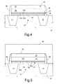
- the structure thus obtained is illustrated in Figure 4 and comprises: a semiconductor body 30; a field insulation region 31 delimiting, inside the semiconductor body 30, an active area 32; and a stack 40, extending on top and at the sides of the active area 32 and on top of the field insulation region 31.
- the stack 40 comprises: a gate oxide region 33; a poly1 region 34, arranged on top of the gate oxide region 33; an interpoly dielectric region 35, arranged on top of the poly1 region 34 and formed by a triple ONO (oxide -nitride-oxide) layer, the triple ONO layer including a first oxide layer 35a, a nitride layer 35b, and a second oxide layer 35c; a poly2 region 36, arranged on top of the interpoly dielectric region 35; and a silicide region 37, for example of tungsten silicide, arranged on top of the poly2 region 36. Spacing regions 38, for example of oxide and/or nitride, extend at the sides of the stack 40.
- the stack 40 has an elongated shape extending transverse to the active area 32; in particular, the stack 40 has a central portion extending on top of the active area 32 and end portions extending on top of the field insulation region 31.
- the source and drain regions 41 are formed, which are illustrated schematically in Figure 3.
- an etch-stop layer 44 deposited, for instance of nitride, completely coating the stack 40 (and hence the silicide region 37 and the spacing regions 38).
- the contact mask is formed, and the contacts are opened.
- a photoresist layer is deposited and defined, so as to have openings where the contacts are to be formed, as illustrated in Figures 3 and 6, showing the resist mask 47 and the contact openings 48.
- the openings for connecting the poly1 region 34 to the poly2 region 36 are designated by 48a.
- the openings 48a are formed on top of the field insulation region 31, outside the active area 32.
- the passivation layer 45 is initially etched employing a dedicated chemistry that is highly selective in respect to nitride. Said etch stops on the etch-stop layer 44 on top of the stack 40. Elsewhere, and hence also at the contacts on the active area, a passivation thickness equal to the height of the gate stack remains. The structure of Figure 7 is thus obtained.
- a second etch is carried out, using once again the resist mask 47 but with different chemical processes so as to remove, in sequence, the etch-stop nitride layer 44 on top of the stack 40, portions of the silicide layer 37, of the poly2 layer 36 and of the interpoly dielectric layer 35, stopping on the poly1 layer 34.
- paths 50 are formed that extend from the surface of the passivation layer 45 as far as the poly1 layer 34.
- the residual portion of the passivation layer 45 on top of the contact opening region in the active area (source and drain) is removed by the etch used for the second oxide layer 35c of the interpoly dielectric 35.
- the etch-stop nitride layer 44 is removed at the contacts, simultaneously with the nitride layer 35b of the interpoly dielectric 35, thus uncovering silicon for source and drain contacts.
- a barrier layer 51 for example of Ti/TiN
- a metal layer 52 for example of tungsten
- the metal layer 52 fills the paths 50 to form, together with the barrier layer 51, first plugs 53 for contacting the various regions of the transistor, and second plugs 53a in the paths 50.
- the metal layer 52 is then removed from the surface of the passivation layer 45.
- metal layer is deposited to obtain metal connection regions (metal 1); if envisaged, connections are formed at more than one metallization level, and the customary final operations of fabrication are carried out.
- the plugs 53a connect the poly1 region 34 and poly2 region 36 by contacting the poly2 region 36 on the sides of the paths 50 and the poly1 region 34 on the bottom of the paths 50.
- the plugs 53a are column-like shaped with a substantially constant cross section without any evident steps due to the staggering between the two masks.
- Connecting the poly1 and poly2 regions through a plug formed in a single opening of the passivation layer 45 and in the stack 40 enables the size of the path 50 to be reduced down to a lithographic minimum, and in particular plugs to be formed of the same size as the plugs used for the active area and for the gate region of the memory cells.
- the contact thus obtained can tolerate possible misalignments between the contact mask 47 and the mask for defining the stack 40 as well as any possible process variations.
- the second etching step etching of layers 34 -37 and 44
- the second etching step is selective with respect to the oxide and, in the case of misalignment, over-etching of the field insulation region 31 is prevented, provided that the area of the plug 53a lies on top of the stack 40.
- a possible partial removal of the poly1 region 34 does not, on the other hand, adversely affect the electrical connection between the regions 34, 36. It follows that the process is reliable and does not present any particular critical aspects.
- Elimination of one mask moreover enables saving on a manufacture step which has a far from negligible cost, and hence a reduction in fabrication costs.
- the number of poly connection plugs 53a may vary, and poly connection plugs 53a may be provided on both sides of the active area 32.
- the same solution may be use d for electrically connecting two polysilicon layers in other types of devices integrated together with dual -polysilicon-layer memory cells.
- the path 50 may be made also on the edge of the stack 40, instead of inside the stack 40.
Landscapes
- Engineering & Computer Science (AREA)
- Manufacturing & Machinery (AREA)
- Internal Circuitry In Semiconductor Integrated Circuit Devices (AREA)
- Thin Film Transistor (AREA)
- Semiconductor Memories (AREA)
Abstract
Description
- Figure 1 illustrates the layout of an MOS transistor made with a dedicated mask for connecting the two polysilicon layers;
- Figure 2 is a cross-sectional view of the transistor of Figure 1;
- Figure 3 illustrates the layout of a first embodiment of the transistor according to the invention; and
- Figures 4 to 9 illustrate cross-sectional views, taken along line IX-IX of Figure 3, in successive manufacturing steps of the transistor of Figure 3.
Claims (16)
- An MOS device comprising a stack (40) and a passivation layer (45) covering said stack, said stack (40) being formed by a first polysilicon region (34) and a second polysilicon region (36) arranged on top of one another and separated by an intermediate dielectric region (35), an electrical connection region (53a) extending through said passivation layer (45) and being in electrical contact with said first and second polysilicon regions (34, 36), characterized in that said electrical connection region (53a) is formed by a column-shaped structure substantially free of steps, which traverses said passivation layer (45), said second polysilicon region (36) and said intermediate dielectric region (35) and terminates in contact with said first polysilicon region (34).
- The MOS device according to claim 1, wherein said electrical connection region (53a) has a substantially constant cross-section.
- The MOS device according to claim 1 or 2, wherein said electrical connection region (53a) extends along a single path (50) which extenmds through said passivation layer (45), said second polysilicon region (36) and said intermediate dielectric region (35), and terminates on said first polysilicon region (34).
- The MOS device according to any one of the preceding c laims, further comprising an etch-stop region (44) of a material highly resistant to etching of said passivation layer (45), on top of said second polysilicon region (36) and covering said stack (40), said electrical connection region (53a) moreover extend ing through said etch-stop region (44).
- The MOS device according to claim 4, wherein said etch -stop region (44) is of silicon nitride, and said passivation layer (45) is of silicon oxide.
- The MOS device according to claim 5, further comprising a silicide region (37) extending laterally between said second polysilicon region (36) and said etch -stop region (44), said electrical connection region (53a) moreover extending through said silicide region (37).
- The MOS device according to any one of the preceding claims, forming an MOS transistor, wherein said stack (40) is a gate region.
- The MOS device according to claim 7, wherein said gate region (40) has an elongated shape having a central portion extending on top of an active area (32) of semiconductor material, and end portions extending on top of a field insulation region (31), wherein said electrical connection region (53a) extends on top of said field insulation region (31).
- A process for manufacturing an MOS device, comprising the steps of:characterized in that, after said step of forming contact paths (50), the step is performed of selectively remov ing portions of said second polysilicon region (36) and said intermediate dielectric region (35) underneath at least one of said contact paths so as to form a poly connection path (50), and said step of filling said contact paths further comprises filling said poly connection path (50), to form a column-shaped structure (53a) substantially free of steps, which extends through said passivation layer (45), said second polysilicon region (36) and said intermediate dielectric region (35), and terminates in contact with said first polysilicon region (34).forming a stack (40) including a first polysilicon region (34), an intermediate dielectric region (35) arranged on top of said first polysilicon region, and a second polysilicon region (36) arranged on top of said intermediate dielectric region;depositing a passivation layer (45) on top of and laterally with respect to said stack (40);forming a contact mask (47) covering said passivation layer (45);forming contact paths (50) in said passivation layer (45); andfilling said contact paths so as to form plugs (53) and an electrical connection region (53a) in electrical contact with said first and second polysilicon regions (34, 36),
- The process according to claim 9, wherein said step of selectively removing portions of said second polysilicon region (36) and said intermediate dielectric region (35) uses said contact mask (47).
- The process according to claim 9 or 10, wherein, prior to depositing a passivation layer (45), a step is carried out of forming an etch-stop region (44) of a material highly resistant to etching of oxide on top of said second polysilicon region (36), and wherein said step of forming at least one poly connection path (50) initially comprises selective removal of said etch-stop region (44) using said contact mask (47).
- The process according to claim 11, wherein the passivation layer (45) is of oxide, and said etch-stop region (44) is of silicon nitride.
- The process according to claim 11 or 12, comprising the step of providing a silicide region (37) between said second polysilicon region (36) and said etch-stop region (44), and said step of selective removal further comprises removing selective portions of said silicide region (37) using said contact mask (47).
- The process according to any one of claims 9 to 13, wherein said step of filling comprises depositing a barrier layer (51) on walls and on the bottom of said contact paths and of said poly connection path (50), and filling said contact paths and said poly connection path with metal material (52).
- The process according to any one of claims 9 to 14, wherein said step of forming a stack (40) comprises forming a gate region of a MOS transistor.
- The process according to claim 15, comprising, prior to said step of forming a stack (40), forming, in a semiconductor material (30), a field insulation region (31) so as to define an active area (32), wherein said step of forming a gate region (40) comprises forming an elongated structure having a central portion extending on top of said active area (32) and end portions extending on top of said field insulation region (31), and wherein said electrical connection region (24) is formed on top of said field insulation region.
Applications Claiming Priority (2)
| Application Number | Priority Date | Filing Date | Title |
|---|---|---|---|
| IT001119A ITTO20021119A1 (en) | 2002-12-24 | 2002-12-24 | MOS DEVICE AND MANUFACTURING PROCEDURE OF |
| ITTO20021119 | 2002-12-24 |
Publications (3)
| Publication Number | Publication Date |
|---|---|
| EP1434257A2 true EP1434257A2 (en) | 2004-06-30 |
| EP1434257A3 EP1434257A3 (en) | 2004-12-15 |
| EP1434257B1 EP1434257B1 (en) | 2010-09-15 |
Family
ID=32448952
Family Applications (1)
| Application Number | Title | Priority Date | Filing Date |
|---|---|---|---|
| EP03104939A Expired - Lifetime EP1434257B1 (en) | 2002-12-24 | 2003-12-23 | Process for manufacturing MOS devices using dual-polysilicon layer technology |
Country Status (4)
| Country | Link |
|---|---|
| US (1) | US7023047B2 (en) |
| EP (1) | EP1434257B1 (en) |
| DE (1) | DE60334188D1 (en) |
| IT (1) | ITTO20021119A1 (en) |
Families Citing this family (3)
| Publication number | Priority date | Publication date | Assignee | Title |
|---|---|---|---|---|
| ITTO20021118A1 (en) | 2002-12-24 | 2004-06-25 | St Microelectronics Srl | MOS DEVICE AND MANUFACTURING PROCEDURE OF |
| US7306552B2 (en) * | 2004-12-03 | 2007-12-11 | Samsung Electronics Co., Ltd. | Semiconductor device having load resistor and method of fabricating the same |
| CN102088001B (en) * | 2009-12-04 | 2013-10-09 | 中芯国际集成电路制造(上海)有限公司 | Flash memory and manufacturing method thereof |
Family Cites Families (7)
| Publication number | Priority date | Publication date | Assignee | Title |
|---|---|---|---|---|
| IT1213249B (en) * | 1984-11-26 | 1989-12-14 | Ates Componenti Elettron | PROCESS FOR THE MANUFACTURE OF INTEGRATED STRUCTURES INCLUDING NON-VOLATILE MEMORY CELLS WITH SELF-ALIGNED SILICON LAYERS AND ASSOCIATED TRANSISTORS. |
| KR940009644B1 (en) * | 1991-11-19 | 1994-10-15 | 삼성전자 주식회사 | Non-volatile semiconductor memory device and manufacturing method thereof |
| JPH104149A (en) * | 1996-06-14 | 1998-01-06 | Oki Electric Ind Co Ltd | Semiconductor memory and its manufacture |
| JP4392867B2 (en) * | 1998-02-06 | 2010-01-06 | 株式会社ルネサステクノロジ | Semiconductor device and manufacturing method thereof |
| EP0996162A1 (en) * | 1998-10-21 | 2000-04-26 | STMicroelectronics S.r.l. | Low resistance contact structure for a select transistor of EEPROM memory cells |
| JP2000311992A (en) * | 1999-04-26 | 2000-11-07 | Toshiba Corp | Nonvolatile semiconductor memory device and method of manufacturing the same |
| US6680514B1 (en) * | 2000-12-20 | 2004-01-20 | International Business Machines Corporation | Contact capping local interconnect |
-
2002
- 2002-12-24 IT IT001119A patent/ITTO20021119A1/en unknown
-
2003
- 2003-12-23 DE DE60334188T patent/DE60334188D1/en not_active Expired - Lifetime
- 2003-12-23 US US10/745,295 patent/US7023047B2/en not_active Expired - Lifetime
- 2003-12-23 EP EP03104939A patent/EP1434257B1/en not_active Expired - Lifetime
Also Published As
| Publication number | Publication date |
|---|---|
| ITTO20021119A1 (en) | 2004-06-25 |
| US20040188759A1 (en) | 2004-09-30 |
| EP1434257B1 (en) | 2010-09-15 |
| DE60334188D1 (en) | 2010-10-28 |
| US7023047B2 (en) | 2006-04-04 |
| EP1434257A3 (en) | 2004-12-15 |
Similar Documents
| Publication | Publication Date | Title |
|---|---|---|
| US6627491B2 (en) | Method of manufacturing non volatile memory device having two charge storage regions | |
| KR19980018838A (en) | A semiconductor device having a tapered isolation insulating film and a method of manufacturing the same. | |
| US7829414B2 (en) | Method for manufacturing non-volatile semiconductor memory device, and non-volatile semiconductor memory device | |
| US6518124B1 (en) | Method of fabricating semiconductor device | |
| KR101432619B1 (en) | Semiconductor device and manufacturing method thereof | |
| US20030049903A1 (en) | Semiconductor device and method of manufacturing the same | |
| US6790721B2 (en) | Metal local interconnect self-aligned source flash cell | |
| KR100232984B1 (en) | Manufacturing Method of Semiconductor Device | |
| US7928494B2 (en) | Semiconductor device | |
| JPH10223770A (en) | Semiconductor device and manufacturing method thereof | |
| JP2001257325A (en) | Semiconductor memory device and method of manufacturing the same | |
| US20050118798A1 (en) | Gate-contact structure and method for forming the same | |
| EP1434257B1 (en) | Process for manufacturing MOS devices using dual-polysilicon layer technology | |
| US7755127B2 (en) | Capacitor in semiconductor device and method of manufacturing the same | |
| US7091570B2 (en) | MOS device and a process for manufacturing MOS devices using a dual-polysilicon layer technology with side contact | |
| US8836008B2 (en) | Semiconductor device and method of manufacturing same | |
| KR20040010061A (en) | Method of fabricating semiconductor device | |
| US7195968B2 (en) | Method of fabricating semiconductor device | |
| US7642595B2 (en) | Nonvolatile semiconductor memory and method of fabrication thereof | |
| US20080197402A1 (en) | Methods of Forming Nonvolatile Memory Devices and Memory Devices Formed Thereby | |
| US6682976B2 (en) | Method for manufacturing a nonvolatile semiconductor memory device | |
| US6350671B1 (en) | Method for autoaligning overlapped lines of a conductive material in integrated electronic circuits | |
| US7432182B2 (en) | Semiconductor device and method for manufacturing the same | |
| JPH088349A (en) | Fabrication of semiconductor device | |
| KR100825770B1 (en) | Self-aligned Common Source Line Fabrication Method in NAND Flash Memory Devices |
Legal Events
| Date | Code | Title | Description |
|---|---|---|---|
| PUAI | Public reference made under article 153(3) epc to a published international application that has entered the european phase |
Free format text: ORIGINAL CODE: 0009012 |
|
| AK | Designated contracting states |
Kind code of ref document: A2 Designated state(s): AT BE BG CH CY CZ DE DK EE ES FI FR GB GR HU IE IT LI LU MC NL PT RO SE SI SK TR |
|
| AX | Request for extension of the european patent |
Extension state: AL LT LV MK |
|
| PUAL | Search report despatched |
Free format text: ORIGINAL CODE: 0009013 |
|
| RTI1 | Title (correction) |
Free format text: MOS DEVICE AND PROCESS FOR MANUFACTURING MOS DEVICES USING DUAL-POLYSILICON LAYER TECHNOLOGY |
|
| AK | Designated contracting states |
Kind code of ref document: A3 Designated state(s): AT BE BG CH CY CZ DE DK EE ES FI FR GB GR HU IE IT LI LU MC NL PT RO SE SI SK TR |
|
| AX | Request for extension of the european patent |
Extension state: AL LT LV MK |
|
| RIC1 | Information provided on ipc code assigned before grant |
Ipc: 7H 01L 27/115 A Ipc: 7H 01L 21/8247 B Ipc: 7H 01L 29/423 B |
|
| 17P | Request for examination filed |
Effective date: 20050610 |
|
| AKX | Designation fees paid |
Designated state(s): DE FR GB IT |
|
| 17Q | First examination report despatched |
Effective date: 20050811 |
|
| RTI1 | Title (correction) |
Free format text: PROCESS FOR MANUFACTURING MOS DEVICES USING DUAL-POLYSILICON LAYER TECHNOLOGY |
|
| RAP1 | Party data changed (applicant data changed or rights of an application transferred) |
Owner name: STMICROELECTRONICS SRL |
|
| GRAP | Despatch of communication of intention to grant a patent |
Free format text: ORIGINAL CODE: EPIDOSNIGR1 |
|
| GRAJ | Information related to disapproval of communication of intention to grant by the applicant or resumption of examination proceedings by the epo deleted |
Free format text: ORIGINAL CODE: EPIDOSDIGR1 |
|
| GRAP | Despatch of communication of intention to grant a patent |
Free format text: ORIGINAL CODE: EPIDOSNIGR1 |
|
| GRAS | Grant fee paid |
Free format text: ORIGINAL CODE: EPIDOSNIGR3 |
|
| GRAA | (expected) grant |
Free format text: ORIGINAL CODE: 0009210 |
|
| AK | Designated contracting states |
Kind code of ref document: B1 Designated state(s): DE FR GB IT |
|
| REG | Reference to a national code |
Ref country code: GB Ref legal event code: FG4D |
|
| REF | Corresponds to: |
Ref document number: 60334188 Country of ref document: DE Date of ref document: 20101028 Kind code of ref document: P |
|
| PG25 | Lapsed in a contracting state [announced via postgrant information from national office to epo] |
Ref country code: IT Free format text: LAPSE BECAUSE OF FAILURE TO SUBMIT A TRANSLATION OF THE DESCRIPTION OR TO PAY THE FEE WITHIN THE PRESCRIBED TIME-LIMIT Effective date: 20100915 |
|
| PLBE | No opposition filed within time limit |
Free format text: ORIGINAL CODE: 0009261 |
|
| STAA | Information on the status of an ep patent application or granted ep patent |
Free format text: STATUS: NO OPPOSITION FILED WITHIN TIME LIMIT |
|
| 26N | No opposition filed |
Effective date: 20110616 |
|
| REG | Reference to a national code |
Ref country code: DE Ref legal event code: R097 Ref document number: 60334188 Country of ref document: DE Effective date: 20110616 |
|
| REG | Reference to a national code |
Ref country code: FR Ref legal event code: PLFP Year of fee payment: 13 |
|
| REG | Reference to a national code |
Ref country code: FR Ref legal event code: PLFP Year of fee payment: 14 |
|
| REG | Reference to a national code |
Ref country code: FR Ref legal event code: PLFP Year of fee payment: 15 |
|
| REG | Reference to a national code |
Ref country code: DE Ref legal event code: R079 Ref document number: 60334188 Country of ref document: DE Free format text: PREVIOUS MAIN CLASS: H01L0027115000 Ipc: H10B0069000000 |
|
| PGFP | Annual fee paid to national office [announced via postgrant information from national office to epo] |
Ref country code: GB Payment date: 20221220 Year of fee payment: 20 Ref country code: FR Payment date: 20221222 Year of fee payment: 20 Ref country code: DE Payment date: 20220527 Year of fee payment: 20 |
|
| REG | Reference to a national code |
Ref country code: DE Ref legal event code: R071 Ref document number: 60334188 Country of ref document: DE |
|
| REG | Reference to a national code |
Ref country code: GB Ref legal event code: PE20 Expiry date: 20231222 |
|
| PG25 | Lapsed in a contracting state [announced via postgrant information from national office to epo] |
Ref country code: GB Free format text: LAPSE BECAUSE OF EXPIRATION OF PROTECTION Effective date: 20231222 |
|
| PG25 | Lapsed in a contracting state [announced via postgrant information from national office to epo] |
Ref country code: GB Free format text: LAPSE BECAUSE OF EXPIRATION OF PROTECTION Effective date: 20231222 |