EP1433249B1 - Compensating method for a pll circuit functioning according to the two-point-modulation and pll circuit provided with a compensating device - Google Patents
Compensating method for a pll circuit functioning according to the two-point-modulation and pll circuit provided with a compensating device Download PDFInfo
- Publication number
- EP1433249B1 EP1433249B1 EP02754420A EP02754420A EP1433249B1 EP 1433249 B1 EP1433249 B1 EP 1433249B1 EP 02754420 A EP02754420 A EP 02754420A EP 02754420 A EP02754420 A EP 02754420A EP 1433249 B1 EP1433249 B1 EP 1433249B1
- Authority
- EP
- European Patent Office
- Prior art keywords
- pll circuit
- signal
- modulation
- frequency
- comparison
- Prior art date
- Legal status (The legal status is an assumption and is not a legal conclusion. Google has not performed a legal analysis and makes no representation as to the accuracy of the status listed.)
- Expired - Fee Related
Links
Images
Classifications
-
- H—ELECTRICITY
- H03—ELECTRONIC CIRCUITRY
- H03C—MODULATION
- H03C3/00—Angle modulation
- H03C3/02—Details
- H03C3/09—Modifications of modulator for regulating the mean frequency
- H03C3/0908—Modifications of modulator for regulating the mean frequency using a phase locked loop
- H03C3/0991—Modifications of modulator for regulating the mean frequency using a phase locked loop including calibration means or calibration methods
-
- H—ELECTRICITY
- H03—ELECTRONIC CIRCUITRY
- H03C—MODULATION
- H03C3/00—Angle modulation
- H03C3/02—Details
- H03C3/09—Modifications of modulator for regulating the mean frequency
- H03C3/0908—Modifications of modulator for regulating the mean frequency using a phase locked loop
- H03C3/0916—Modifications of modulator for regulating the mean frequency using a phase locked loop with frequency divider or counter in the loop
- H03C3/0925—Modifications of modulator for regulating the mean frequency using a phase locked loop with frequency divider or counter in the loop applying frequency modulation at the divider in the feedback loop
-
- H—ELECTRICITY
- H03—ELECTRONIC CIRCUITRY
- H03C—MODULATION
- H03C3/00—Angle modulation
- H03C3/02—Details
- H03C3/09—Modifications of modulator for regulating the mean frequency
- H03C3/0908—Modifications of modulator for regulating the mean frequency using a phase locked loop
- H03C3/0916—Modifications of modulator for regulating the mean frequency using a phase locked loop with frequency divider or counter in the loop
- H03C3/0933—Modifications of modulator for regulating the mean frequency using a phase locked loop with frequency divider or counter in the loop using fractional frequency division in the feedback loop of the phase locked loop
-
- H—ELECTRICITY
- H03—ELECTRONIC CIRCUITRY
- H03C—MODULATION
- H03C3/00—Angle modulation
- H03C3/02—Details
- H03C3/09—Modifications of modulator for regulating the mean frequency
- H03C3/0908—Modifications of modulator for regulating the mean frequency using a phase locked loop
- H03C3/0941—Modifications of modulator for regulating the mean frequency using a phase locked loop applying frequency modulation at more than one point in the loop
-
- H—ELECTRICITY
- H03—ELECTRONIC CIRCUITRY
- H03C—MODULATION
- H03C3/00—Angle modulation
- H03C3/02—Details
- H03C3/09—Modifications of modulator for regulating the mean frequency
- H03C3/0908—Modifications of modulator for regulating the mean frequency using a phase locked loop
- H03C3/095—Modifications of modulator for regulating the mean frequency using a phase locked loop applying frequency modulation to the loop in front of the voltage controlled oscillator
-
- H—ELECTRICITY
- H03—ELECTRONIC CIRCUITRY
- H03L—AUTOMATIC CONTROL, STARTING, SYNCHRONISATION, OR STABILISATION OF GENERATORS OF ELECTRONIC OSCILLATIONS OR PULSES
- H03L7/00—Automatic control of frequency or phase; Synchronisation
- H03L7/06—Automatic control of frequency or phase; Synchronisation using a reference signal applied to a frequency- or phase-locked loop
- H03L7/08—Details of the phase-locked loop
- H03L7/085—Details of the phase-locked loop concerning mainly the frequency- or phase-detection arrangement including the filtering or amplification of its output signal
- H03L7/089—Details of the phase-locked loop concerning mainly the frequency- or phase-detection arrangement including the filtering or amplification of its output signal the phase or frequency detector generating up-down pulses
- H03L7/0891—Details of the phase-locked loop concerning mainly the frequency- or phase-detection arrangement including the filtering or amplification of its output signal the phase or frequency detector generating up-down pulses the up-down pulses controlling source and sink current generators, e.g. a charge pump
- H03L7/0893—Details of the phase-locked loop concerning mainly the frequency- or phase-detection arrangement including the filtering or amplification of its output signal the phase or frequency detector generating up-down pulses the up-down pulses controlling source and sink current generators, e.g. a charge pump the up-down pulses controlling at least two source current generators or at least two sink current generators connected to different points in the loop
-
- H—ELECTRICITY
- H03—ELECTRONIC CIRCUITRY
- H03L—AUTOMATIC CONTROL, STARTING, SYNCHRONISATION, OR STABILISATION OF GENERATORS OF ELECTRONIC OSCILLATIONS OR PULSES
- H03L7/00—Automatic control of frequency or phase; Synchronisation
- H03L7/06—Automatic control of frequency or phase; Synchronisation using a reference signal applied to a frequency- or phase-locked loop
- H03L7/16—Indirect frequency synthesis, i.e. generating a desired one of a number of predetermined frequencies using a frequency- or phase-locked loop
- H03L7/18—Indirect frequency synthesis, i.e. generating a desired one of a number of predetermined frequencies using a frequency- or phase-locked loop using a frequency divider or counter in the loop
- H03L7/197—Indirect frequency synthesis, i.e. generating a desired one of a number of predetermined frequencies using a frequency- or phase-locked loop using a frequency divider or counter in the loop a time difference being used for locking the loop, the counter counting between numbers which are variable in time or the frequency divider dividing by a factor variable in time, e.g. for obtaining fractional frequency division
- H03L7/1974—Indirect frequency synthesis, i.e. generating a desired one of a number of predetermined frequencies using a frequency- or phase-locked loop using a frequency divider or counter in the loop a time difference being used for locking the loop, the counter counting between numbers which are variable in time or the frequency divider dividing by a factor variable in time, e.g. for obtaining fractional frequency division for fractional frequency division
- H03L7/1976—Indirect frequency synthesis, i.e. generating a desired one of a number of predetermined frequencies using a frequency- or phase-locked loop using a frequency divider or counter in the loop a time difference being used for locking the loop, the counter counting between numbers which are variable in time or the frequency divider dividing by a factor variable in time, e.g. for obtaining fractional frequency division for fractional frequency division using a phase accumulator for controlling the counter or frequency divider
Definitions
- the invention relates to a matching method for a two-point modulation PLL circuit and a two-point modulation designed PLL circuit with a matching device.
- a cost-effective realization of a transmitter concept for transceivers in mobile radio systems offer transmitters which have a modulator operating according to the known two-point modulation.
- a PLL (Phase Locked Loop) circuit is used as a frequency synthesizer and used for phase or frequency modulation of a high-frequency signal.
- An impressing of the modulation signal in the PLL circuit is usually carried out via a programmable frequency divider contained in the feedback branch of the PLL loop.
- a digital modulation signal is used and used for continuous reprogramming of the digital frequency divider.
- This form of modulation which is also referred to as one-point modulation, is known, for example, from the patents US 4,965,531 . US 6,008,703 and US 6,044,124 known.
- the bandwidth of the circuit is designed much smaller than is required for the transmission of the modulated data. Therefore, in addition to the purely digital modulation, analog modulation is also used to compensate for the limited bandwidth.
- analog modulation is also used to compensate for the limited bandwidth.
- the simultaneous impressing of a digital and an analog modulation signal in a PLL circuit is referred to as two-point modulation.
- the impressing of the digital and analog modulation signals takes place at two different points of the PLL circuit.
- Essential for the functioning of the two-point modulation is that in addition to the temporal in-phase a high degree of coincidence of the amplitudes of the two modulation signals used is needed. Due to manufacturing tolerances of the components for the analog modulation, however, fluctuations in the modulation slope and the amplitude level of the modulation occur. For this reason, it is necessary to make an amplitude adjustment between the analog and the digital modulation signal after the production of the PLL circuit.
- a two-point modulator and a method for phase and frequency modulation with a PLL circuit is disclosed in German Offenlegungsschrift DE 199 29 167 A1 described.
- the modulation takes place here on the one hand at a point of the PLL circuit, which results in a high-pass transmission behavior for the modulation frequency.
- the modulation takes place at a second point of the PLL circuit, at which a low-pass transmission behavior results for the modulation frequency.
- the modulation with low-pass transmission behavior takes place digitally in a frequency divider in the feedback path of the PLL circuit.
- One known method for equalizing a PLL circuit with two-point modulation is to impress the two-point modulation of the circuit in the steady state and to receive and demodulate the transmitted signal with an external measuring receiver. Depending on the demodulation result obtained, an adjustment of the digital and analog modulation signals is performed.
- VCO Voltage Controlled Oscillator
- this adjustment must be made for each channel. For a larger number of channels, this results in a correspondingly long measurement duration.
- the adjustment information must be stored in a memory.
- Another disadvantage is the fact that the influence of temperature changes is not taken into account in this method.
- the receiving as well as the demodulating of the signal generated by the PLL circuit can also be performed by the receiving part of the transceiver.
- this increases the circuit complexity in a disadvantageous manner, since this would require a complete second PLL circuit in the receiver.
- WO 99/07065 is described a matching method for a PLL, which operates on the principle of two-point modulation.
- the PLL is tuned to different frequencies by specifying different divisor values N and the corresponding voltage values are recorded at the input of the VCO. From the value pairs determined in this way, the characteristic of the VCO is calculated. The characteristic curve is evaluated by means of a processor and scaling values are determined for setting the modulation deviation of the analog modulation signal.
- the object of the invention is to provide a compensation method for a PLL circuit, with which a fast and accurate amplitude adjustment between the digital and the analog modulation signal can be achieved. Furthermore, the invention aims to provide a PLL circuit with an adjustment device, in which a fast and accurate amplitude adjustment of the modulation signals can be achieved with a relatively simple circuit construction.
- the PLL circuit is adjusted to a first frequency by impressing a first digital modulation signal. Subsequently, a second digital modulation signal is impressed into the PLL circuit, wherein the PLL circuit adjusts to a deviating from the first frequency second frequency.
- a difference signal which is characteristic of the change of a control signal of a frequency-generating unit of the PLL circuit caused by the two digital modulation signals, is generated and coupled out of the PLL circuit.
- the difference signal is compared with a comparison signal, which is characteristic for a modulation deviation of an analog modulation signal, and depending on the deviation determined in the comparison, the modulation deviation is changed such that the deviation is eliminated.
- the demodulation of the output signal generated by the PLL circuit is omitted for balancing purposes, since for compensation a deviation between two digital modulation signals is used, which is represented in a difference signal characteristic of the deviation. Furthermore, it can be achieved that a relatively accurate and fast matching can be performed.
- An advantageous embodiment of the adjustment method according to the invention is characterized in that the first digital modulation signal is impressed such that the PLL circuit is adjusted to a first frequency, which is formed by subtracting a frequency of a variably selectable digital modulation of a channel center frequency. Unless then by impressing the second digital Modulation signal the PLL circuit is adjusted to a second frequency, which is formed by adding the frequency of the variably selectable, digital modulation and channel center frequency, a preferred embodiment characterized in that a voltage corresponding to the analog modulation signal voltage value for comparing with the difference signal corresponding voltage value multiplied by a factor of 2. It can thereby be achieved that an analog voltage value corresponding to the differential signal can be made relatively large and thus deviations between the digital modulation and the analog modulation can be compensated relatively precisely.
- a main path of the PLL circuit is connected in parallel with a tuning path which contributes to the generation of control signals.
- the compensation path is activated at least during the impressing of the second digital modulation signal.
- the main path of the PLL circuit is deactivated after impressing the first digital modulation signal by setting a current generated by a first charge pump in the main path to the value zero. This ensures that a voltage corresponding to the first digital modulation signal remains substantially constant at a tuning input of a VCO during the following steps (second injection step and possibly matching step).
- maintaining the voltage generated at the tuning input of the VCO at the first injection step may generally be accomplished in other ways as well.
- Another advantageous embodiment is characterized in that the main path of the PLL circuit after the impressing of the first digital modulation signal is kept active and a current through the charge pump in the main path of the PLL circuit is set such that the voltage at the tuning input of the VCO is kept substantially constant. It can thereby be achieved that a change in the voltage (generated during the first injection step) at the tuning input of the VCO due to leakage currents in the main path during the adjustment is prevented.
- a compensation path is connected in parallel with a main path of the PLL circuit, which comprises a decoupling means for generating a difference signal which is characteristic of the change of a control signal of a frequency-generating unit when impressing different digital modulation signals into the PLL circuit.
- the adjustment path comprises a comparison unit for comparing the difference signal with a comparison signal which is characteristic of a modulation deviation of an analog modulation signal, and a modulation unit which varies the modulation deviation in dependence on an output signal of the comparison unit.
- the differential signal can be applied to a modulation input of a VCO of the PLL circuit via a first switch. Furthermore, it can be provided that the balancing path a second switch, in the closed position, the comparison signal is applied to an input of the comparison unit.
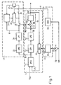
- a PLL circuit 1 operating according to the two-point modulation (FIG. 1) is electrically connected to a modulation device 2 and a tuning path 3.
- the loop filter 13 is designed as a low-pass filter, whereby higher-frequency signal components are smoothed.
- the VCO 14 represents the vibration generating device in the PLL circuit 1, and has a summing point 141 and a frequency generating unit 142.
- the DIV 15 can, for example, as fractional-N Frequency divider be executed, whereby a frequency division is made possible by a non-integer.
- the modulation device 2 To process a modulation signal MS, the modulation device 2 has a programming unit 21 and a digital-to-analog converter (DAC) 22.
- DAC digital-to-analog converter
- the balancing path 3 has a second charge pump (CP2) 33 and a second loop filter (LP2) 34 connected downstream of the charge pump 33. Furthermore, a comparison unit 31 and an analog modulation unit 32 are arranged in the alignment path 3. Depending on the adjustment process performed, the comparison unit 31 and the analog modulation unit 32 are electrically connected via a first switch 35 to a modulation input ME of the VCO 14 of the PLL circuit 1. Via a second switch 36, the output of the analog modulation unit 32 can be coupled back to a second input of the comparison unit 31. This signal path between the modulation unit 32 and the comparison unit 31 furthermore has a multiplier 37.
- a modulation signal MS which is embodied as a digital signal in the exemplary embodiment, is based on a summation point 4 on a PLL frequency synthesis underlying Carrier signal TS added.
- the resulting signal 5 is applied to an input of the programming unit 21.
- the programming unit 21 which is embodied in the exemplary embodiment as a sigma-delta modulator, generates at its output a first digital modulation signal 6, which is applied to a second input of the DIV 15.
- the digital modulation signal 6 indicates a divider ratio 1: N 1 , wherein N 1 represents an integer.
- the modulation signal MS is impressed into the feedback path via the DIV 15 at a frequency division ratio determined by the modulation (variable).
- a first frequency division signal 7 is generated, which is applied to the first input of the PFD 11.
- a reference signal with a corresponding reference frequency F REF is a reference signal with a corresponding reference frequency F REF .
- the reference frequency F REF can be generated for example by a quartz crystal , not shown.
- a signal is generated at the output of the PFD 11, which characterizes the frequency and / or phase difference between the reference signal and the first frequency division signal 7.
- This output signal 9 of the PFD 11 is used to drive the charge pump 12.
- a current is generated, which is dependent on the signal 9, with which the charge pump 12 is driven. With the current generated in the charge pump 12, the loop filter 13 is charged.
- the output signal of the loop filter 13 is a voltage signal and is applied to the tuning input TE of the VCO 14.
- an output signal AS is generated, which is applied to the first input of the DIV 15 and which is modulated by the first digital modulation signal 6.
- the first digital modulation signal 6 is input with a first constant divider ratio 1: N 1 .
- the divider ratio 1: N 1 is such that the PLL circuit 1 adjusts to a first frequency F 1 corresponding to a channel center frequency f less a digital modulation pitch ⁇ f Dig .
- the adjustment path 3 is deactivated, the second loop filter (LP2) 34 being precharged to the fixed voltage value zero.
- the switches 35 and 36 are in the positions shown in Figure 1, which are referred to in both switches 35 and 36 as closed.
- the main path of the PLL circuit 1 is deactivated by the current from the charge pump 12 is set to the fixed value zero and the control loop is opened with it. It is ensured by the integrating behavior of the loop filter 13 that the voltage V 1 at the tuning input TE of the VCO 14 or at a summation point 141 remains virtually unchanged. This applies at least for the duration of the subsequent adjustment process. Furthermore, now the balancing path 3, that is, the second charge pump 33 and the second loop filter 34 is activated and thereby the control loop via the balancing path. 3 closed. The switch position of the two switches 35 and 36 remains unchanged.
- the programming unit 21 is reprogrammed, so that at the output of the programming unit 21, a second digital modulation signal 6 'is generated, which indicates a second constant divider ratio 1: N 2 .
- the PLL circuit is thus adjusted to the second frequency F 2 . Since the voltage value V 1 continues to be present at the tuning input TE, a voltage value V 2 , which corresponds to twice the digital modulation deviation 2 ⁇ f Dig , is established at the modulation input ME of the VCO 14.
- the modulation signal MS is converted by the DAC 22 into an analog modulation signal 8 in a third step and is applied to a second input of the analog modulation unit 32.
- the voltage value corresponding to this frequency F 3 at the modulation input ME must be half as high as the voltage value in the balanced state Be V 2 .
- this voltage value is tapped off at the output of the modulation unit 32 and applied after a duplication in the multiplier 37 as a comparison signal 8 'to a second input of the comparison unit 31.
- the voltage value V 2 of the difference signal 9 ' is applied simultaneously to a first input of the comparison unit 31, which is designed as a comparator in the embodiment.
- the switch positions are still unchanged, that is, the comparison unit 31 and the analog modulation unit 32 are decoupled by the switch position of the first switch 35 from the modulation input ME of the VCO 14.
- a deviation, determined in the comparison unit 31, between the voltage value V 2 of the difference signal 9 'and the corresponding voltage value of the comparison signal 8' is eliminated by changing the modulation deviation of the analog modulation signal provided at the output of the analog modulation unit 32.
- the switch 35 is switched, the switch 36 is opened and the charge pump 33 and the loop filter 34 are deactivated.
- the main path of the PLL circuit 1 is activated.
- the PLL circuit 1 for the two-point modulation is now balanced and can start its operation.
- the digital and the analog modulation signal overlap and it results in a frequency-independent transmission behavior of the PLL circuit 1 as a result of the described adjustment process.
- the balancing of the signals applied to the comparison unit 31 can take place, for example, in an iterative process. In this case, an approximate adjustment of the modulation amplitudes takes place with alternate updating of the comparison signal 8 'and evaluation of the subsequently obtained changed output signal of the comparison unit 31. When the voltage difference at the comparison unit 31 has been eliminated, the adjustment between digital and analog modulation deviation is achieved.
Abstract
Description
Die Erfindung betrifft ein Abgleichverfahren für eine nach der Zwei-Punkt-Modulation arbeitende PLL-Schaltung und eine nach dem Prinzip der Zwei-Punkt-Modulation ausgelegte PLL-Schaltung mit einer Abgleichvorrichtung.The invention relates to a matching method for a two-point modulation PLL circuit and a two-point modulation designed PLL circuit with a matching device.
Eine aufwandsgünstige Realisierung eines Senderkonzepts für Transceiver in Mobilfunksystemen bieten Sender, welche einen nach der bekannten Zwei-Punkt-Modulation arbeitenden Modulator aufweisen. Eine PLL (Phase Locked Loop = Nachlaufsynchronisation)-Schaltung wird dabei als Frequenzsynthesizer eingesetzt und zur Phasen- oder Frequenzmodulation eines hochfrequenten Signals verwendet.A cost-effective realization of a transmitter concept for transceivers in mobile radio systems offer transmitters which have a modulator operating according to the known two-point modulation. A PLL (Phase Locked Loop) circuit is used as a frequency synthesizer and used for phase or frequency modulation of a high-frequency signal.
Ein Einprägen des Modulationssignals in die PLL-Schaltung erfolgt üblicherweise über einen im Rückkoppelzweig der PLL-Schleife enthaltenen programmierbaren Frequenzteiler. Dabei wird ein digitales Modulationssignal verwendet und zum fortwährenden Umprogrammieren des digitalen Frequenzteilers eingesetzt. Diese Form der Modulation, die auch als Ein-Punkt-Modulation bezeichnet wird, ist beispielsweise aus den Patentschriften
Um ein geringes Rauschen der PLL-Schaltung zu erreichen, wird die Bandbreite der Schaltung deutlich kleiner ausgelegt, als es für die Übertragung der modulierten Daten erforderlich ist. Daher wird zusätzlich zu der rein digitalen Modulation auch eine analoge Modulation zur Kompensation der beschränkten Bandbreite eingesetzt. Das gleichzeitige Einprägen eines digitalen und eines analogen Modulationssignals in eine PLL-Schaltung wird als Zwei-Punkt-Modulation bezeichnet.In order to achieve a low noise of the PLL circuit, the bandwidth of the circuit is designed much smaller than is required for the transmission of the modulated data. Therefore, in addition to the purely digital modulation, analog modulation is also used to compensate for the limited bandwidth. The simultaneous impressing of a digital and an analog modulation signal in a PLL circuit is referred to as two-point modulation.
Das Einprägen der digitalen und analogen Modulationssignale erfolgt an zwei unterschiedlichen Punkten der PLL-Schaltung. Wesentlich für die Funktionsweise der Zwei-Punkt-Modulation ist, dass neben der zeitlichen Gleichphasigkeit ein hohes Maß an Übereinstimmung der Amplituden der beiden verwendeten Modulationssignale benötigt wird. Aufgrund von Herstellungstoleranzen der Komponenten für die analoge Modulation treten jedoch Schwankungen in der Modulationssteilheit sowie der Amplitudenhöhe der Modulation auf. Aus diesem Grund ist es erforderlich, nach der Herstellung der PLL-Schaltung einen Amplitudenabgleich zwischen dem analogen und dem digitalen Modulationssignal vorzunehmen.The impressing of the digital and analog modulation signals takes place at two different points of the PLL circuit. Essential for the functioning of the two-point modulation is that in addition to the temporal in-phase a high degree of coincidence of the amplitudes of the two modulation signals used is needed. Due to manufacturing tolerances of the components for the analog modulation, however, fluctuations in the modulation slope and the amplitude level of the modulation occur. For this reason, it is necessary to make an amplitude adjustment between the analog and the digital modulation signal after the production of the PLL circuit.
Sollen zudem Temperatureinflüsse berücksichtigt werden, muss ein derartiger Abgleich vor jedem Sendevorgang durchgeführt werden.If temperature influences are also to be taken into account, such an adjustment must be carried out before each transmission process.
Ein Zwei-Punkt-Modulator sowie ein Verfahren zur Phasen- und Frequenzmodulation mit einer PLL-Schaltung ist in der deutschen Offenlegungsschrift
Ein bekanntes Verfahren zum Abgleichen einer PLL-Schaltung mit Zwei-Punkt-Modulation besteht darin, die Zwei-Punkt-Modulation der Schaltung im eingeschwungenen Zustand aufzuprägen und mit einem externen Mess-Empfänger das ausgesendete Signal zu empfangen und zu demodulieren. Abhängig von dem erhaltenen Demodulationsergebnis wird ein Abgleich der digitalen und analogen Modulationssignale vorgenommen. Aufgrund des nicht-linearen Verhaltens des schwingungserzeugenden Glieds - eines spannungsgesteuerten Oszillators VCO (Voltage Controlled Oscillator) - der PLL-Schaltung hinsichtlich der Frequenz als Funktion der Steuerspannung, muss dieser Abgleich jedoch für jeden Kanal vorgenommen werden. Für eine größere Anzahl an Kanälen resultiert daraus eine entsprechend lange Messdauer. Zusätzlich müssen die Abgleichinformationen in einem Speicher abgelegt werden. Ein weiterer Nachteil ist darin zu sehen, dass der Einfluss von Temperaturänderungen bei diesem Verfahren nicht berücksichtigt wird.One known method for equalizing a PLL circuit with two-point modulation is to impress the two-point modulation of the circuit in the steady state and to receive and demodulate the transmitted signal with an external measuring receiver. Depending on the demodulation result obtained, an adjustment of the digital and analog modulation signals is performed. However, due to the non-linear behavior of the vibration generating element - a Voltage Controlled Oscillator (VCO) - of the PLL circuit in terms of frequency as a function of control voltage, this adjustment must be made for each channel. For a larger number of channels, this results in a correspondingly long measurement duration. In addition, the adjustment information must be stored in a memory. Another disadvantage is the fact that the influence of temperature changes is not taken into account in this method.
Das Empfangen sowie das Demodulieren des von der PLL-Schaltung erzeugten Signals kann auch durch das Empfangsteil des Transceivers vorgenommen werden. Dadurch erhöht sich allerdings der Schaltungsaufwand in nachteiliger Weise, da hierfür eine vollständige zweite PLL-Schaltung im Empfänger erforderlich wäre.The receiving as well as the demodulating of the signal generated by the PLL circuit can also be performed by the receiving part of the transceiver. However, this increases the circuit complexity in a disadvantageous manner, since this would require a complete second PLL circuit in the receiver.
In der Schrift
Aufgabe der Erfindung ist es, ein Abgleichverfahren für eine PLL-Schaltung zu schaffen, mit dem ein schneller und genauer Amplitudenabgleich zwischen dem digitalen und dem analogen Modulationssignal erreicht werden kann. Ferner zielt die Erfindung darauf ab, eine PLL-Schaltung mit einer Abgleichvorrichtung zu schaffen, bei der ein schneller und genauer Amplitudenabgleich der Modulationssignale mit einem relativ einfachen Schaltungsaufbau erreicht werden kann.The object of the invention is to provide a compensation method for a PLL circuit, with which a fast and accurate amplitude adjustment between the digital and the analog modulation signal can be achieved. Furthermore, the invention aims to provide a PLL circuit with an adjustment device, in which a fast and accurate amplitude adjustment of the modulation signals can be achieved with a relatively simple circuit construction.
Diese Aufgabenstellung wird durch ein Abgleichverfahren, das die Schritte nach Patentanspruch 1 aufweist, und durch eine PLL-Schaltung mit einer Abgleichvorrichtung, die die Merkmale nach Patentanspruch 9 aufweist, gelöst.This object is achieved by a balancing method having the steps according to claim 1, and by a PLL circuit with a balancing device having the features according to claim 9 solved.
Bei einem Abgleichverfahren für eine nach der Zwei-Punkt-Modulation arbeitende PLL-Schaltung wird die PLL-Schaltung durch Einprägen eines ersten digitalen Modulationssignals auf eine erste Frequenz eingeregelt. Anschließend wird ein zweites digitales Modulationssignal in die PLL-Schaltung eingeprägt, wobei die PLL-Schaltung auf eine von der ersten Frequenz abweichende zweite Frequenz einregelt. Ein Differenzsignal, welches charakteristisch für die durch die beiden digitalen Modulationssignale bewirkte Änderung eines Steuersignals einer frequenzerzeugenden Einheit der PLL-Schaltung ist, wird erzeugt und aus der PLL-Schaltung ausgekoppelt. Das Differenzsignal wird mit einem Vergleichssignal, welches charakteristisch für einen Modulationshub eines analogen Modulationssignals ist, verglichen und abhängig von der bei dem Vergleich ermittelten Abweichung wird der Modulationshub derart geändert, dass die Abweichung beseitigt wird.In an alignment method for a two-point modulation PLL circuit, the PLL circuit is adjusted to a first frequency by impressing a first digital modulation signal. Subsequently, a second digital modulation signal is impressed into the PLL circuit, wherein the PLL circuit adjusts to a deviating from the first frequency second frequency. A difference signal, which is characteristic of the change of a control signal of a frequency-generating unit of the PLL circuit caused by the two digital modulation signals, is generated and coupled out of the PLL circuit. The difference signal is compared with a comparison signal, which is characteristic for a modulation deviation of an analog modulation signal, and depending on the deviation determined in the comparison, the modulation deviation is changed such that the deviation is eliminated.
Dadurch kann bei dem erfindungsgemäßen Abgleichverfahren erreicht werden, dass das Demodulieren des von der PLL-Schaltung erzeugten Ausgangssignals zu Abgleichzwecken entfällt, da zum Abgleichen auf eine Abweichung zwischen zwei digitalen Modulationssignalen zurückgegriffen wird, die in einem für die Abweichung charakteristischen Differenzsignal dargestellt wird. Des Weiteren kann dadurch erreicht werden, dass ein relativ genaues und schnelles Abgleichen durchgeführt werden kann.As a result, it can be achieved in the balancing method according to the invention that the demodulation of the output signal generated by the PLL circuit is omitted for balancing purposes, since for compensation a deviation between two digital modulation signals is used, which is represented in a difference signal characteristic of the deviation. Furthermore, it can be achieved that a relatively accurate and fast matching can be performed.
Ein vorteilhaftes Ausführungsbeispiel des erfindungsgemäßen Abgleichverfahrens kennzeichnet sich dadurch, dass das erste digitale Modulationssignal so eingeprägt wird, dass die PLL-Schaltung auf eine erste Frequenz eingeregelt wird, die durch das Subtrahieren einer Frequenz eines variabel wählbaren, digitalen Modulationshubs von einer Kanalmittenfrequenz gebildet wird. Sofern dann durch das Einprägen des zweiten digitalen Modulationssignals die PLL-Schaltung auf eine zweite Frequenz eingeregelt wird, die durch das Addieren der Frequenz des variabel wählbaren, digitalen Modulationshubs und der Kanalmittenfrequenz gebildet wird, kennzeichnet sich eine bevorzugte Ausführungsvariante dadurch, dass ein dem analogen Modulationssignal entsprechender Spannungswert zum Vergleichen mit dem dem Differenzsignal entsprechenden Spannungswert mit dem Faktor 2 multipliziert wird. Dadurch kann erreicht werden, dass ein dem Differenzsignal entsprechender analoger Spannungswert relativ groß ausgebildet werden kann und dadurch Abweichungen zwischen der digitalen Modulation und der analogen Modulation relativ genau ausgeglichen werden können.An advantageous embodiment of the adjustment method according to the invention is characterized in that the first digital modulation signal is impressed such that the PLL circuit is adjusted to a first frequency, which is formed by subtracting a frequency of a variably selectable digital modulation of a channel center frequency. Unless then by impressing the second digital Modulation signal the PLL circuit is adjusted to a second frequency, which is formed by adding the frequency of the variably selectable, digital modulation and channel center frequency, a preferred embodiment characterized in that a voltage corresponding to the analog modulation signal voltage value for comparing with the difference signal corresponding voltage value multiplied by a factor of 2. It can thereby be achieved that an analog voltage value corresponding to the differential signal can be made relatively large and thus deviations between the digital modulation and the analog modulation can be compensated relatively precisely.
Gemäß einer bevorzugten Auslegung ist einem Hauptpfad der PLL-Schaltung ein zur Steuersignalerzeugung beitragender Abgleichpfad parallel geschaltet. In diesem Fall kennzeichnet sich eine vorteilhafte Verfahrensvariante dadurch, dass der Abgleichpfad zumindest während des Einprägens des zweiten digitalen Modulationssignals aktiviert ist.According to a preferred embodiment, a main path of the PLL circuit is connected in parallel with a tuning path which contributes to the generation of control signals. In this case, an advantageous variant of the method is characterized in that the compensation path is activated at least during the impressing of the second digital modulation signal.
Ferner kann in vorteilhafter Weise vorgesehen sein, dass der Hauptpfad der PLL-Schaltung nach dem Einprägen des ersten digitalen Modulationssignals deaktiviert wird, indem ein von einer ersten Ladungspumpe im Hauptpfad erzeugter Strom auf den Wert Null gesetzt wird. Dadurch wird erreicht, dass eine dem ersten digitalen Modulationssignal entsprechende Spannung an einem Tuning-Eingang eines VCO während der folgenden Schritte (zweiter Einprägeschritt und ggf. Abgleichschritt) im wesentlichen konstant bleibt.Furthermore, it can be provided in an advantageous manner that the main path of the PLL circuit is deactivated after impressing the first digital modulation signal by setting a current generated by a first charge pump in the main path to the value zero. This ensures that a voltage corresponding to the first digital modulation signal remains substantially constant at a tuning input of a VCO during the following steps (second injection step and possibly matching step).
Das Aufrechterhalten der beim ersten Einprägeschritt an dem Tuning-Eingang des VCO erzeugten Spannung kann im allgemeinen jedoch auch auf andere Weise realisiert werden. Ein weiteres vorteilhaftes Ausführungsbeispiel kennzeichnet sich dadurch, dass der Hauptpfad der PLL-Schaltung nach dem Einprägen des ersten digitalen Modulationssignals aktiv gehalten wird und ein Strom durch die Ladungspumpe im Hauptpfad der PLL-Schaltung derart eingestellt wird, dass die Spannung am Tuning-Eingang des VCO im wesentlichen konstant gehalten wird. Dadurch kann erreicht werden, dass ein Ändern der (während des ersten Einprägeschrittes erzeugten) Spannung am Tuning-Eingang des VCO aufgrund von Leckströmen im Hauptpfad während des Abgleichens verhindert wird.However, maintaining the voltage generated at the tuning input of the VCO at the first injection step may generally be accomplished in other ways as well. Another advantageous embodiment is characterized in that the main path of the PLL circuit after the impressing of the first digital modulation signal is kept active and a current through the charge pump in the main path of the PLL circuit is set such that the voltage at the tuning input of the VCO is kept substantially constant. It can thereby be achieved that a change in the voltage (generated during the first injection step) at the tuning input of the VCO due to leakage currents in the main path during the adjustment is prevented.
Ein weiterer Aspekt der Erfindung betrifft eine PLL-Schaltung, die für das Einprägen eines analogen und eines digitalen Modulationssignals nach dem Prinzip der Zwei-Punkt-Modulation ausgebildet ist. Einem Hauptpfad der PLL-Schaltung ist ein Abgleichpfad parallel geschaltet, der ein Auskoppelmittel zur Erzeugung eines Differenzsignals umfasst, welches für die Änderung eines Steuersignals einer frequenzerzeugenden Einheit bei Einprägen unterschiedlicher digitaler Modulationssignale in die PLL-Schaltung charakteristisch ist. Weiterhin umfasst der Abgleichpfad eine Vergleichseinheit zum Vergleichen des Differenzsignals mit einem Vergleichssignal, welches charakteristisch für einen Modulationshub eines analogen Modulationssignals ist, und eine Modulationseinheit, die den Modulationshub in Abhängigkeit von einem Ausgangssignal der Vergleichseinheit verändert.Another aspect of the invention relates to a PLL circuit, which is designed for the impressing of an analog and a digital modulation signal according to the principle of two-point modulation. A compensation path is connected in parallel with a main path of the PLL circuit, which comprises a decoupling means for generating a difference signal which is characteristic of the change of a control signal of a frequency-generating unit when impressing different digital modulation signals into the PLL circuit. Furthermore, the adjustment path comprises a comparison unit for comparing the difference signal with a comparison signal which is characteristic of a modulation deviation of an analog modulation signal, and a modulation unit which varies the modulation deviation in dependence on an output signal of the comparison unit.
Durch die erfindungsgemäße PLL-Schaltung mit dem Hauptpfad und dem parallel geschalteten Abgleichpfad ist ein relativ einfacher und aufwandsarmer Schaltungsaufbau realisiert, mit dem ein schneller und genauer Abgleich des digitalen und des analogen Modulationssignals durchgeführt werden kann.By means of the PLL circuit according to the invention with the main path and the parallel adjustment path, a relatively simple and low-cost circuit configuration is realized with which a fast and accurate adjustment of the digital and the analog modulation signal can be performed.
Bei einem vorteilhaften Ausführungsbeispiel kann vorgesehen sein, dass über einen ersten Schalter das Differenzsignal an einen Modulationseingang eines VCO der PLL-Schaltung anlegbar ist. Weiterhin kann vorgesehen sein, dass der Abgleichpfad einen zweiten Schalter aufweist, in dessen geschlossener Stellung das Vergleichssignal an einem Eingang der Vergleichseinheit anliegt.In an advantageous embodiment, it can be provided that the differential signal can be applied to a modulation input of a VCO of the PLL circuit via a first switch. Furthermore, it can be provided that the balancing path a second switch, in the closed position, the comparison signal is applied to an input of the comparison unit.
Weitere vorteilhafte Ausgestaltungen des Abgleichverfahrens und der PLL-Schaltung sind in den Unteransprüchen angegeben.Further advantageous embodiments of the adjustment method and the PLL circuit are specified in the subclaims.
Die Erfindung wird nachfolgend anhand eines Ausführungsbeispiels unter Bezugnahme auf die Zeichnung näher erläutert. Es zeigen:
- Fig. 1
- ein Blockschaltbild einer erfindungsgemäßen PLL-Schaltung mit einer Abgleichvorrichtung, und
- Fig. 2
- ein schematisches Ablaufdiagramm des erfindungsgemäßen Abgleichverfahrens.
- Fig. 1
- a block diagram of a PLL circuit according to the invention with a balancing device, and
- Fig. 2
- a schematic flow diagram of the balancing method according to the invention.
Eine nach der Zwei-Punkt-Modulation arbeitende PLL-Schaltung 1 (Fig. 1) ist mit einer Modulationsvorrichtung 2 und einem Abgleichpfad 3 elektrisch verbunden. Die PLL-Schaltung 1 weist in ihrem Hauptpfad einen Phasendetektor (PFD = Phase Frequency Detector) 11, eine erste Ladungspumpe (CP1 = Charge Pump 1) 12, ein erstes Schleifenfilter (LP1 = Loop Filter 1) 13 und einen spannungsgesteuerten Oszillator (VCO = Voltage Controlled Oscillator) 14 auf. Das Schleifenfilter 13 ist als Tiefpassfilter ausgeführt, wodurch höherfrequente Signalanteile geglättet werden. Der VCO 14 stellt das schwingungserzeugende Bauelement in der PLL-Schaltung 1 dar und weist einen Summationspunkt 141 und eine frequenzerzeugende Einheit 142 auf. Über einen Rückkoppelpfad, welcher sich vom Ausgang des VCO 14 zu einem Eingang des PFD 11 erstreckt und in dem ein programmierbarer Frequenzteiler (DIV = Divider) 15 angeordnet ist, wird die PLL-Schaltung 1 geschlossen. Der DIV 15 kann beispielsweise als Fraktional-N Frequenzteiler ausgeführt sein, wodurch auch eine Frequenzteilung durch eine nicht ganze Zahl ermöglicht wird.A PLL circuit 1 operating according to the two-point modulation (FIG. 1) is electrically connected to a modulation device 2 and a tuning path 3. The PLL circuit 1 has in its main path a phase detector (PFD = Phase Frequency Detector) 11, a first charge pump (CP1 = charge pump 1) 12, a first loop filter (LP1 = Loop Filter 1) 13 and a voltage controlled oscillator (VCO = Voltage Controlled Oscillator) 14. The
Zur Aufbereitung eines Modulationssignals MS weist die Modulationsvorrichtung 2 eine Programmiereinheit 21 und einen Digital-Analog-Wandler (DAC = Digital Analog Converter) 22 auf.To process a modulation signal MS, the modulation device 2 has a programming unit 21 and a digital-to-analog converter (DAC) 22.
Parallel zum Hauptpfad der PLL-Schaltung 1 ist der Abgleichpfad 3 geschaltet. Der Abgleichpfad 3 weist eine zweite Ladungspumpe (CP2) 33 und ein der Ladungspumpe 33 nachgeschaltetes zweites Schleifenfilter (LP2) 34 auf. Weiterhin ist eine Vergleichseinheit 31 und eine analoge Modulationseinheit 32 im Abgleichpfad 3 angeordnet. Abhängig vom durchgeführten Abgleichvorgang wird die Vergleichseinheit 31 und die analoge Modulationseinheit 32 über einen ersten Schalter 35 mit einem Modulationseingang ME des VCO 14 der PLL-Schaltung 1 elektrisch verbunden. Über einen zweiten Schalter 36 ist der Ausgang der analogen Modulationseinheit 32 mit einem zweiten Eingang der Vergleichseinheit 31 rückkoppelbar. Dieser Signalweg zwischen der Modulationseinheit 32 und der Vergleichseinheit 31 weist des Weiteren einen Multiplizierer 37 auf.Parallel to the main path of the PLL circuit 1 of the adjustment path 3 is connected. The balancing path 3 has a second charge pump (CP2) 33 and a second loop filter (LP2) 34 connected downstream of the
Bei der Zwei-Punkt-Modulation wird der PLL-Schaltung 1 über die Modulationsvorrichtung 2 ein analoges und ein digitales Modulationssignal eingeprägt. Da das analoge Modulationssignal im Gegensatz zum digitalen Modulationssignal, welches aufgrund seiner diskreten Natur keine Toleranzen aufweist, drift- und toleranzbehaftet ist, ist es erforderlich, die beiden Modulationssignale hinsichtlich ihrer Amplituden abzugleichen.In the two-point modulation of the PLL circuit 1 via the modulation device 2, an analog and a digital modulation signal is impressed. Since the analog modulation signal, in contrast to the digital modulation signal, which has no tolerances due to its discrete nature, drift and tolerance, it is necessary to match the two modulation signals in terms of their amplitudes.
Ein Modulationssignal MS, welches im Ausführungsbeispiel als digitales Signal ausgeführt ist, wird an einem Summationspunkt 4 auf ein der PLL-Frequenzsynthese zugrunde liegendes Trägersignal TS addiert. Das resultierende Signal 5 liegt an einem Eingang der Programmiereinheit 21 an.A modulation signal MS, which is embodied as a digital signal in the exemplary embodiment, is based on a summation point 4 on a PLL frequency synthesis underlying Carrier signal TS added. The resulting signal 5 is applied to an input of the programming unit 21.
Die Programmiereinheit 21, die im Ausführungsbeispiel als Sigma-Delta Modulator ausgeführt ist, erzeugt an ihrem Ausgang ein erstes digitales Modulationssignal 6, welches an einen zweiten Eingang des DIV 15 anliegt. Das digitale Modulationssignal 6 gibt dabei ein Teilerverhältnis 1:N1 an, wobei N1 eine ganze Zahl darstellt. Dadurch wird das Modulationssignal MS mit einem durch die Modulation bestimmten (variablen) Frequenzteilungsverhältnis über den DIV 15 in den Rückkoppelzweig eingeprägt. Am Ausgang des DIV 15 wird ein erstes Frequenzteilungssignal 7 erzeugt, welches am ersten Eingang des PFD 11 anliegt.The programming unit 21, which is embodied in the exemplary embodiment as a sigma-delta modulator, generates at its output a first
An einem zweiten Eingang des PFD 11 liegt ein Referenzsignal mit einer entsprechenden Referenzfrequenz FREF an. Die Referenzfrequenz FREF kann beispielsweise durch einen nicht dargestellten Schwingquarz erzeugt werden. Dadurch wird am Ausgang des PFD 11 ein Signal erzeugt, das die Frequenz- und/oder Phasendifferenz zwischen dem Referenzsignal und dem ersten Frequenzteilungssignal 7 charakterisiert. Dieses Ausgangssignal 9 des PFD 11 wird zur Ansteuerung der Ladungspumpe 12 verwendet. In der Ladungspumpe 12 wird ein Strom erzeugt, der abhängig von dem Signal 9 ist, mit dem die Ladungspumpe 12 angesteuert wird. Mit dem in der Ladungspumpe 12 erzeugten Strom wird das Schleifenfilter 13 aufgeladen. Das Ausgangssignal des Schleifenfilters 13 ist ein Spannungssignal und liegt an dem Tuning-Eingang TE des VCO 14 an.At a second input of the
Am Ausgang des VCO 14 wird ein Ausgangssignal AS erzeugt, das am ersten Eingang des DIV 15 anliegt und welches durch das erste digitale Modulationssignal 6 moduliert ist.At the output of the
Das Abgleichverfahren wird nachfolgend anhand der PLL-Schaltung gemäß Figur 1 erläutert:The balancing method is explained below with reference to the PLL circuit according to FIG. 1:
In einem ersten Schritt wird das erste digitale Modulationssignal 6 mit einem ersten konstanten Teilerverhältnis 1:N1 eingegeben. Das Teilerverhältnis 1:N1 ist derart, dass die PLL-Schaltung 1 auf eine erste Frequenz F1 einregelt, die einer Kanalmittenfrequenz f abzüglich einem digitalen Modulationshub ΔfDig entspricht.In a first step, the first
Indem die PLL-Schaltung 1 auf die Frequenz F1 = f - ΔfDig eingeregelt wird, stellt sich am Tuning-Eingang TE des VCO 14 ein Spannungswert V1 ein, der dieser Frequenz F1 entspricht, z.B. im Falle einer linearen Frequenz-Spannungs-Kennlinie des VCO 14 zu dieser Frequenz F1 proportional ist.By the PLL circuit 1 is adjusted to the frequency F 1 = f - .DELTA.f Dig , sets at the tuning input TE of the
Während dieses Einregelns der PLL-Schaltung 1 auf die Frequenz F1 ist der Abgleichpfad 3 deaktviert, wobei das zweite Schleifenfilter (LP2) 34 auf den festen Spannungswert Null vorgeladen ist. Die Schalter 35 und 36 sind in den in Figur 1 dargestellten Positionen, die bei beiden Schaltern 35 und 36 als geschlossen bezeichnet werden.During this adjustment of the PLL circuit 1 to the frequency F 1 , the adjustment path 3 is deactivated, the second loop filter (LP2) 34 being precharged to the fixed voltage value zero. The
Nachdem das Einregeln der PLL-Schaltung 1 auf die Frequenz F1 abgeschlossen ist, wird in einem zweiten Schritt der Hauptpfad der PLL-Schaltung 1 deaktiviert, indem der Strom von der Ladungspumpe 12 auf den festen Wert Null eingestellt und die Regelschleife damit geöffnet wird. Dabei wird durch das integrierende Verhalten des Schleifenfilters 13 gewährleistet, dass die Spannung V1 am Tuning-Eingang TE des VCO 14 bzw. an einem Summationspunkt 141 praktisch unverändert bleibt. Dies gilt zumindest für die Dauer des nachfolgenden Abgleichvorgangs. Ferner wird nun der Abgleichpfad 3, das heißt die zweite Ladungspumpe 33 und das zweite Schleifenfilter 34, aktiviert und dadurch die Regelschleife über den Abgleichpfad 3 geschlossen. Die Schalterstellung der beiden Schalter 35 und 36 bleibt dabei unverändert.After the adjustment of the PLL circuit 1 to the frequency F 1 is completed, in a second step, the main path of the PLL circuit 1 is deactivated by the current from the
Anschließend wird die Programmiereinheit 21 umprogrammiert, so dass am Ausgang der Programmiereinheit 21 ein zweites digitales Modulationssignal 6' erzeugt wird, welches ein zweites konstantes Teilerverhältnis 1:N2 angibt.Subsequently, the programming unit 21 is reprogrammed, so that at the output of the programming unit 21, a second digital modulation signal 6 'is generated, which indicates a second constant divider ratio 1: N 2 .
Das zweite Teilerverhältnis 1:N2 wird derart eingestellt, dass das Ausgangssignal AS am VCO 14 eine zweite Frequenz F2 = f + ΔfDig aufweist. Die PLL-Schaltung wird somit auf die zweite Frequenz F2 eingeregelt. Da am Tuning-Eingang TE weiterhin der Spannungswert V1 anliegt, stellt sich am Modulationsseingang ME des VCO 14 ein Spannungswert V2 ein, der dem doppelten digitalen Modulationshub 2ΔfDig entspricht.The second divider ratio 1: N 2 is adjusted such that the output signal AS at the
Dieser Spannungswert V2 resultiert daraus, dass die Ausgangsfrequenz am VCO 14 der zweiten Frequenz F2 entspricht, auf die die PLL-Schaltung 1 eingeregelt wird. An der frequenzerzeugenden Einheit 142 liegt daher ein Steuersignal SS an, dessen Spannung V3 diese Frequenz F2 erzeugt. Aufgrund der Summationsbedingung am Summationspunkt 141 sowie der festen Spannung V1 am Tuning-Eingang TE, ergibt sich daher am Modulationseingang ME ein Spannungswert V2(2ΔfDig) = V3(f + ΔfDig) - V1(f - ΔfDig).This voltage value V 2 results from the fact that the output frequency at the
Zum Vergleichen des Differenzsignals 9' am Ausgang des zweiten Tiefpassfilters 34 mit einem analogen Modulationssignal wird in einem dritten Schritt das Modulationssignal MS durch den DAC 22 in ein analoges Modulationssignal 8 gewandelt und liegt an einem zweiten Eingang der analogen Modulationseinheit 32 an. Das analoge Modulationssignal 8 bewirkt eine Frequenz F3 = f + ΔfAna am Ausgang des VCO. Der dieser Frequenz F3 entsprechende Spannungswert am Modulationseingang ME muss im abgeglichenen Zustand halb so groß wie der Spannungswert V2 sein. Zum Vergleichen mit dem Spannungswert V2 wird dieser Spannungswert am Ausgang der Modulationseinheit 32 abgegriffen und nach einer Verdoppelung in dem Multiplizierer 37 als Vergleichssignal 8' an einen zweiten Eingang der Vergleichseinheit 31 angelegt.To compare the difference signal 9 'at the output of the second low-
Der Spannungswert V2 des Differenzsignals 9' liegt gleichzeitig an einem ersten Eingang der Vergleichseinheit 31 an, die im Ausführungsbeispiel als Komparator ausgeführt ist. Die Schalterpositionen sind weiterhin unverändert, das heißt die Vergleichseinheit 31 und die analoge Modulationseinheit 32 sind durch die Schalterstellung des ersten Schalters 35 vom Modulationseingang ME des VCO 14 entkoppelt.The voltage value V 2 of the difference signal 9 'is applied simultaneously to a first input of the comparison unit 31, which is designed as a comparator in the embodiment. The switch positions are still unchanged, that is, the comparison unit 31 and the
Eine in der Vergleichseinheit 31 ermittelte Abweichung zwischen dem Spannungswert V2 des Differenzsignals 9' und dem entsprechenden Spannungswert des Vergleichssignals 8' wird beseitigt, indem der Modulationshub des am Ausgang der analogen Modulationseinheit 32 bereitgestellten analogen Modulationssignals verändert wird.A deviation, determined in the comparison unit 31, between the voltage value V 2 of the difference signal 9 'and the corresponding voltage value of the comparison signal 8' is eliminated by changing the modulation deviation of the analog modulation signal provided at the output of the
Alternativ kann die dem Differenzsignal 9' entsprechende Spannung V2 am Eingang der Vergleichseinheit 31, beispielsweise durch einen Kondensator, gespeichert werden und anschließend mit dem Spannungswert des Vergleichssignals 8' verglichen werden.Alternatively, the voltage V 2 corresponding to the difference signal 9 'can be stored at the input of the comparison unit 31, for example by a capacitor, and then compared with the voltage value of the comparison signal 8'.
Nachdem der Abgleichvorgang abgeschlossen ist, wird der Schalter 35 umgeschaltet, der Schalter 36 geöffnet und die Ladungspumpe 33 und das Schleifenfilter 34 deaktiviert. Der Hauptpfad der PLL-Schaltung 1 wird aktiviert.After the adjustment process is completed, the
Die PLL-Schaltung 1 für die Zwei-Punkt-Modulation ist nun abgeglichen und kann ihren Betrieb aufnehmen. Das digitale und das analoge Modulationssignal überlagern sich dabei und es ergibt sich infolge des beschriebenen Abgleichvorgangs ein frequenzunabhängiges Übertragungsverhalten der PLL-Schaltung 1.The PLL circuit 1 for the two-point modulation is now balanced and can start its operation. The digital and the analog modulation signal overlap and it results in a frequency-independent transmission behavior of the PLL circuit 1 as a result of the described adjustment process.
Das Erzeugen des Vergleichssignals 8' kann auch in der Vergleichseinheit 31 oder in der analogen Modulationseinheit 32 durchgeführt werden.The generation of the comparison signal 8 'can also be carried out in the comparison unit 31 or in the
Wird als Modulationssignal MS ein analoges Signal verwendet, kann die Modulationsvorrichtung 2 beispielsweise auch derart ausgeführt sein, dass der DAC 22 nicht benötigt wird aber dafür eine entsprechende Signalwandlung im digitalen Modulationspfad durchgeführt wird.If an analog signal is used as the modulation signal MS, the modulation device 2 may, for example, also be embodied such that the
Das Abgleichen der an die Vergleichseinheit 31 angelegten Signale kann beispielsweise in einem iterativen Prozess erfolgen. In diesem Fall erfolgt ein approximativer Abgleich der Modulationsamplituden mit wechselweiser Aktualisierung des Vergleichssignals 8' und Bewertung des daraufhin erhaltenen, geänderten Ausgangssignals der Vergleichseinheit 31. Bei erfolgter Beseitigung der Spannungsdifferenz an der Vergleichseinheit 31 ist der Abgleich zwischen digitalem und analogem Modulationshub erreicht.The balancing of the signals applied to the comparison unit 31 can take place, for example, in an iterative process. In this case, an approximate adjustment of the modulation amplitudes takes place with alternate updating of the comparison signal 8 'and evaluation of the subsequently obtained changed output signal of the comparison unit 31. When the voltage difference at the comparison unit 31 has been eliminated, the adjustment between digital and analog modulation deviation is achieved.
Es kann auch vorgesehen sein, dass während des Abgleichens der Hauptpfad der PLL-Schaltung 1 aktiv gehalten wird, indem die erste Ladungspumpe 12 mit einem kleinen Strom betrieben wird. Aufgrund des reduzierten Stroms der ersten Ladungspumpe 12 kann der Hauptpfad der PLL-Schaltung 1 der Modulation nicht folgen und die Spannung am Tuning-Eingang TE des VCO 14 bleibt konstant. Dadurch kann erreicht werden, dass ein Spannungsverlust am Tuning-Eingang TE des VCO 14 bedingt durch Leckströme, die bei einem deaktivierten Hauptpfad auftreten können, kompensiert werden.It may also be provided that, during balancing, the main path of the PLL circuit 1 is kept active by operating the
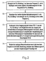
In Fig. 2 ist ein schematisches Ablaufdiagramm des Abgleichverfahrens aufgezeigt. In dem ersten Verfahrensschritt S1 wird die PLL-Schaltung 1 (Fig. 1) 1 auf eine Frequenz F1 = f - ΔfDig eingeregelt, indem das erste digitale Modulationssignal 6 in den Hauptpfad der PLL-Schaltung 1 eingeprägt wird. Im nachfolgenden zweiten Verfahrensschritt S2 wird das zweite digitale Modulationssignal 6' in die PLL-Schaltung 1 eingeprägt und die PLL-Schaltung auf die Frequenz F2 = f + ΔfDig eingeregelt. Ein Ausgangssignal 9 wird aus der PLL-Schaltung 1 ausgekoppelt und ein Differenzsignal 9' erzeugt, welches charakteristisch für die durch die beiden digitalen Modulationssignale 6 und 6' bewirkte Spannungsänderung eines Steuersignals SS am Eingang der frequenzerzeugenden Einheit 142 ist. Das Differenzsignal 9' wird mit dem dem analogen Modulationssignal 8 proportionalen Vergleichssignal 8' gemäß Verfahrensschritt S3 verglichen. Die bei dem Vergleichen ermittelte Abweichung zwischen dem Differenzsignal 9' und dem Vergleichssignal 8' wird beseitigt, indem der analoge Modulationshub entsprechend dem Verfahrensschritt S4 verändert wird.In Fig. 2 is a schematic flow diagram of the adjustment method is shown. In the first method step S1, the PLL circuit 1 (FIG. 1) 1 is adjusted to a frequency F 1 = f -Δf Dig by impressing the first
Claims (12)
- Compensating method for a PLL circuit (1) that functions according to two-point modulation, with the following steps:(a) injecting a first digital modulation signal (6) into the PLL circuit (1), the latter being tuned to the first frequency (F1),(b) injecting a second digital modulation signal (6') into the PLL circuit (1), the latter being tuned to a second frequency (F2), which is different from the first frequency (F1),(c) coupling out a differential signal (9'), which is characteristic of the change of a control signal (SS) of a frequency-generating unit (142) of the PLL circuit (1) that is brought about by the two modulation signals (6, 6'),(d) comparing the differential signal (9') with a comparison signal (8'), which is characteristic of a modulation amplitude (ΔfAna) of an analog modulation signal, and(e) changing the modulation amplitude (ΔfAna) in such a way that a deviation between the differential signal (9') and the comparison signal (8') that is determined in the comparison is eliminated.
- Method according to Claim 1, characterized in that the injection of the first digital modulation signal (6) causes the PLL circuit (1) to be tuned to a first frequency (F1), which is formed, by subtracting a frequency of a variably selectable, digital modulation amplitude (ΔfDig) from a channel center frequency (f).
- Method according to either of Claims 1 and 2, characterized in that the injection of the second digital modulation signal (6') causes the PLL circuit (1) to be tuned to a second frequency (F2), which is formed by adding the frequency of the variably selectable, digital modulation amplitude (ΔfDig) and the channel center frequency (f).
- Method according to one of the preceding claims, characterized in that a voltage value (V2) corresponding to the analog modulation amplitude is multiplied by a factor of 2 for the comparison with the voltage value corresponding to the differential signal (9').
- Method according to one of the preceding claims, characterized in that a compensating path (3) contributing to the control signal generation is connected in parallel with a main path of the PLL circuit (1), with the step of:- activating the compensating path (3) at least during the injection of the second digital modulation signal (6').
- Method according to Claim 5, characterized by the step of:- deactivating the main path of the PLL circuit (1) after the injection of the first digital modulation signal (6), in that a current generated by a first charge pump (12) in the main path is set to the value of zero.
- Method according to Claim 5, characterized in that the main path of the PLL circuit (1) is kept active during the compensation and a current is set by a charge pump (12) in the main path of the PLL circuit (1) in such a way that the voltage (V1) at a tuning input (TE) of a VCO (14) of the PLL circuit (1) is kept substantially constant.
- Method according to one of the preceding claims, characterized in that the first digital modulation signal (6) and the second digital modulation signal (6') are injected via a frequency divider DIV (15) arranged in the feedback path of the PLL circuit (1).
- PLL circuit, which is designed for the injection of an analog modulation signal and a digital modulation signal according to two-point modulation, characterized in that connected in parallel with a main path of the PLL circuit (1) is a compensating path (3), which- comprises a coupling-out means (33, 34) for generating a differential signal (9'), which is used for the change of a control signal (SS) of a frequency-generating unit (142) of the PLL circuit (1) when different digital modulation signals (6, 6') are injected into the PLL circuit (1),- comprises a comparison unit (31) for comparing the differential signal (9') with a comparison signal (8'), which is used for a modulation amplitude (ΔfAna) of an analog modulation signal (8), and- comprises a modulation unit (32), which changes the modulation amplitude (ΔfAna) of the analog modulation signal (8) in dependence on an output signal of the comparison unit (31).
- PLL circuit according to Claim 9, characterized in that the coupling-out means (33, 34) comprises a charge pump (33) and a loop filter (34) connected downstream of the charge pump (33).
- PLL circuit according to either of Claims 9 and 10, characterized by a first switch (35), by means of which the differential signal (9') can be applied to a modulation input (ME) of a VCO (14) of the PLL circuit (1).
- PLL circuit according to one of Claims 9 to 11, characterized by a second switch (36), in the closed position of which the comparison signal (8') is present at an input of the comparison unit (31).
Applications Claiming Priority (3)
| Application Number | Priority Date | Filing Date | Title |
|---|---|---|---|
| DE10147963A DE10147963A1 (en) | 2001-09-28 | 2001-09-28 | Adjustment method for a PLL circuit working according to the two-point principle and PLL circuit with an adjustment device |
| DE10147963 | 2001-09-28 | ||
| PCT/DE2002/002709 WO2003032493A2 (en) | 2001-09-28 | 2002-07-24 | Compensating method for a pll circuit that functions according to the two-point principle, and pll circuit provided with a compensating device |
Publications (2)
| Publication Number | Publication Date |
|---|---|
| EP1433249A2 EP1433249A2 (en) | 2004-06-30 |
| EP1433249B1 true EP1433249B1 (en) | 2007-09-05 |
Family
ID=7700692
Family Applications (1)
| Application Number | Title | Priority Date | Filing Date |
|---|---|---|---|
| EP02754420A Expired - Fee Related EP1433249B1 (en) | 2001-09-28 | 2002-07-24 | Compensating method for a pll circuit functioning according to the two-point-modulation and pll circuit provided with a compensating device |
Country Status (5)
| Country | Link |
|---|---|
| US (1) | US7154347B2 (en) |
| EP (1) | EP1433249B1 (en) |
| CN (1) | CN1559104A (en) |
| DE (2) | DE10147963A1 (en) |
| WO (1) | WO2003032493A2 (en) |
Families Citing this family (27)
| Publication number | Priority date | Publication date | Assignee | Title |
|---|---|---|---|---|
| DE10207544A1 (en) * | 2002-02-22 | 2003-09-18 | Infineon Technologies Ag | Method for matching a two-point modulator and two-point modulator with a matching device |
| DE10330822A1 (en) * | 2003-07-08 | 2005-02-10 | Infineon Technologies Ag | Two-point modulator for high frequency (HF) transceiver, e.g. in mobile radio, with phase control loop (PLL) operable at different reference frequencies, with digital signal processor provides modulation signal |
| JP3934585B2 (en) * | 2003-08-22 | 2007-06-20 | 松下電器産業株式会社 | Wideband modulation PLL, wideband modulation PLL timing error correction system, modulation timing error correction method, and wireless communication apparatus adjustment method including wideband modulation PLL |
| TWI373925B (en) * | 2004-02-10 | 2012-10-01 | Tridev Res L L C | Tunable resonant circuit, tunable voltage controlled oscillator circuit, tunable low noise amplifier circuit and method of tuning a resonant circuit |
| US7333582B2 (en) * | 2004-03-02 | 2008-02-19 | Matsushita Electric Industrial Co., Ltd. | Two-point frequency modulation apparatus, wireless transmitting apparatus, and wireless receiving apparatus |
| WO2006068237A1 (en) * | 2004-12-24 | 2006-06-29 | Matsushita Electric Industrial Co., Ltd. | Phase modulating apparatus, communication device, mobile wireless unit, and phase modulating method |
| US7289004B2 (en) * | 2005-08-15 | 2007-10-30 | Motorola, Inc. | Dual port modulator |
| US7672645B2 (en) | 2006-06-15 | 2010-03-02 | Bitwave Semiconductor, Inc. | Programmable transmitter architecture for non-constant and constant envelope modulation |
| KR100810386B1 (en) * | 2007-02-12 | 2008-03-04 | 삼성전자주식회사 | Device and method for mixing frequency of transmission in wireless terminal |
| EP2045911A1 (en) * | 2007-10-05 | 2009-04-08 | The Swatch Group Research and Development Ltd. | Method of self-calibrating a frequency synthesiser with FSK modulation at two points |
| EP2220761B1 (en) * | 2007-11-02 | 2011-03-23 | ST-Ericsson SA | Pll calibration |
| US8428212B2 (en) * | 2008-01-30 | 2013-04-23 | Intel Mobile Communications GmbH | Frequency synthesis using upconversion PLL processes |
| DE602008004158D1 (en) * | 2008-10-03 | 2011-02-03 | Swatch Group Res & Dev Ltd | Self-calibration procedure of a frequency generator with two-point FSK modulation |
| US7902891B1 (en) * | 2009-10-09 | 2011-03-08 | Panasonic Corporation | Two point modulator using voltage control oscillator and calibration processing method |
| US8339165B2 (en) * | 2009-12-07 | 2012-12-25 | Qualcomm Incorporated | Configurable digital-analog phase locked loop |
| US8446191B2 (en) | 2009-12-07 | 2013-05-21 | Qualcomm Incorporated | Phase locked loop with digital compensation for analog integration |
| US8358178B2 (en) * | 2009-12-17 | 2013-01-22 | Electronics And Telecommunications Research Institute | Phase modulation apparatus and method |
| JP5694696B2 (en) * | 2010-07-15 | 2015-04-01 | ラピスセミコンダクタ株式会社 | Frequency synthesizer device and modulation frequency displacement adjustment method |
| JP5557634B2 (en) * | 2010-07-20 | 2014-07-23 | ルネサスエレクトロニクス株式会社 | High frequency signal processor |
| CN102882518A (en) * | 2012-10-24 | 2013-01-16 | 四川和芯微电子股份有限公司 | Phase-locked loop system and implementation method for same |
| TW201422468A (en) * | 2012-12-06 | 2014-06-16 | Vehicle Semiconductor Technology Company Ltd E | Universal control circuit of generator voltage regulator for all kinds of automobiles |
| TWI630798B (en) * | 2014-02-07 | 2018-07-21 | 美商線性科技股份有限公司 | Arbitrary phase trajectory frequency synthesizer |
| US9391625B1 (en) * | 2015-03-24 | 2016-07-12 | Innophase Inc. | Wideband direct modulation with two-point injection in digital phase locked loops |
| EP3168983B1 (en) * | 2015-11-13 | 2018-10-17 | The Swatch Group Research and Development Ltd. | Method for calibrating a frequency synthesizer with two-point fsk modulation |
| CN107005244B (en) * | 2017-02-08 | 2020-05-05 | 香港应用科技研究院有限公司 | Gain calibration of direct modulation synthesizer using look-up table search by decreasing count of overflow counter |
| CN113129977B (en) * | 2019-12-30 | 2023-12-15 | 群联电子股份有限公司 | Signal receiving circuit, memory storage device and signal receiving method |
| CN115134204B (en) * | 2022-07-08 | 2023-06-09 | 海能达通信股份有限公司 | Modulation circuit, modulation calibration method and modulation system |
Family Cites Families (12)
| Publication number | Priority date | Publication date | Assignee | Title |
|---|---|---|---|---|
| US4965531A (en) * | 1989-11-22 | 1990-10-23 | Carleton University | Frequency synthesizers having dividing ratio controlled by sigma-delta modulator |
| US5027087A (en) * | 1990-02-02 | 1991-06-25 | Motorola, Inc. | Fast-switching frequency synthesizer |
| US5483203A (en) * | 1994-11-01 | 1996-01-09 | Motorola, Inc. | Frequency synthesizer having modulation deviation correction via presteering stimulus |
| US6008703A (en) * | 1997-01-31 | 1999-12-28 | Massachusetts Institute Of Technology | Digital compensation for wideband modulation of a phase locked loop frequency synthesizer |
| US5983077A (en) * | 1997-07-31 | 1999-11-09 | Ericsson Inc. | Systems and methods for automatic deviation setting and control in radio transmitters |
| US6044124A (en) * | 1997-08-22 | 2000-03-28 | Silicon Systems Design Ltd. | Delta sigma PLL with low jitter |
| US6034573A (en) * | 1997-10-30 | 2000-03-07 | Uniden San Diego Research & Development Center, Inc. | Method and apparatus for calibrating modulation sensitivity |
| EP0961412B1 (en) * | 1998-05-29 | 2004-10-06 | Motorola Semiconducteurs S.A. | Frequency synthesiser |
| DE19929167A1 (en) * | 1999-06-25 | 2000-12-28 | Siemens Ag | Modulator and method for phase or frequency modulation with a PLL circuit |
| DE10108636A1 (en) * | 2001-02-22 | 2002-09-19 | Infineon Technologies Ag | Adjustment method and adjustment device for PLL circuit for two-point modulation |
| US6734749B2 (en) * | 2001-05-29 | 2004-05-11 | Telefonaktiebolaget Lm Ericsson (Publ) | Direct modulated phase-locked loop |
| DE10207544A1 (en) * | 2002-02-22 | 2003-09-18 | Infineon Technologies Ag | Method for matching a two-point modulator and two-point modulator with a matching device |
-
2001
- 2001-09-28 DE DE10147963A patent/DE10147963A1/en not_active Ceased
-
2002
- 2002-07-24 CN CNA028189914A patent/CN1559104A/en active Pending
- 2002-07-24 WO PCT/DE2002/002709 patent/WO2003032493A2/en active IP Right Grant
- 2002-07-24 EP EP02754420A patent/EP1433249B1/en not_active Expired - Fee Related
- 2002-07-24 US US10/490,604 patent/US7154347B2/en not_active Expired - Fee Related
- 2002-07-24 DE DE50210859T patent/DE50210859D1/en not_active Expired - Lifetime
Also Published As
| Publication number | Publication date |
|---|---|
| US20050046488A1 (en) | 2005-03-03 |
| US7154347B2 (en) | 2006-12-26 |
| DE10147963A1 (en) | 2003-04-30 |
| CN1559104A (en) | 2004-12-29 |
| DE50210859D1 (en) | 2007-10-18 |
| EP1433249A2 (en) | 2004-06-30 |
| WO2003032493A3 (en) | 2003-09-25 |
| WO2003032493A2 (en) | 2003-04-17 |
Similar Documents
| Publication | Publication Date | Title |
|---|---|---|
| EP1433249B1 (en) | Compensating method for a pll circuit functioning according to the two-point-modulation and pll circuit provided with a compensating device | |
| EP1362413B1 (en) | Compensation method and compensating device for a pll circuit for two-point modulation | |
| DE19954255B4 (en) | Phase Lock Loop and related procedure | |
| DE60036426T2 (en) | Direct digital frequency synthesis that enables troubleshooting | |
| DE19838096C2 (en) | Fractional phase locked loop | |
| DE10257185B3 (en) | Phase-locked loop with sigma-delta modulator having feedback path representing complex transmission function in Laplace plane | |
| EP1402624B1 (en) | Two-point modulator comprising a pll circuit and a simplified digital pre-filtering system | |
| DE60022159T2 (en) | Transmitter with closed feedback for modulation | |
| DE3202733C2 (en) | ||
| DE10330822A1 (en) | Two-point modulator for high frequency (HF) transceiver, e.g. in mobile radio, with phase control loop (PLL) operable at different reference frequencies, with digital signal processor provides modulation signal | |
| DE102004050411B4 (en) | Modulator with controlled transmission bandwidth and corresponding method for controlling the transmission bandwidth | |
| WO2003069770A2 (en) | A point-modulator with a pll circuit | |
| EP1356651B1 (en) | Compensation method for a transceiver using two-point modulation | |
| DE4424364C2 (en) | Reference oscillator with low phase noise | |
| EP1476939B1 (en) | Method for adjusting a two-level modulator and two-level modulator with an adjusting device | |
| EP1236270B1 (en) | Transmitting device | |
| DE102004014204B4 (en) | Phase-locked loop and method for phase correction of a frequency-controllable oscillator | |
| EP0868784A1 (en) | Combining oscillator with a phase-indexed control circuit for a radio receiver | |
| DE3931513C2 (en) | ||
| DE10309335A1 (en) | Phase-locked loop for frequency synthesis e.g. in mobile radio, controls oscillator with time-averaged fraction rational value of digital controls signal related to quantization step | |
| EP0667061A1 (en) | Pll system | |
| DE10100555B4 (en) | Circuit arrangement for generating a phase-locked frequency-modulated carrier frequency signal | |
| EP4062531A1 (en) | Device and method for transmitting data | |
| EP0332087A1 (en) | Frequency modulator | |
| DE10241991A1 (en) | Phase-locked loop with variable bandwidth, has constant ratio of variable division values of frequency dividers provided in forward and feedback paths |
Legal Events
| Date | Code | Title | Description |
|---|---|---|---|
| PUAI | Public reference made under article 153(3) epc to a published international application that has entered the european phase |
Free format text: ORIGINAL CODE: 0009012 |
|
| 17P | Request for examination filed |
Effective date: 20040325 |
|
| AK | Designated contracting states |
Kind code of ref document: A2 Designated state(s): DE FI FR GB IT SE |
|
| GRAP | Despatch of communication of intention to grant a patent |
Free format text: ORIGINAL CODE: EPIDOSNIGR1 |
|
| RTI1 | Title (correction) |
Free format text: COMPENSATING METHOD FOR A PLL CIRCUIT FUNCTIONING ACCORDING TO THE TWO-POINT-MODULATION AND PLL CIRCUIT PROVIDED WITH A COMPENSATING DEVICE |
|
| GRAS | Grant fee paid |
Free format text: ORIGINAL CODE: EPIDOSNIGR3 |
|
| GRAA | (expected) grant |
Free format text: ORIGINAL CODE: 0009210 |
|
| AK | Designated contracting states |
Kind code of ref document: B1 Designated state(s): DE |
|
| REF | Corresponds to: |
Ref document number: 50210859 Country of ref document: DE Date of ref document: 20071018 Kind code of ref document: P |
|
| PLBE | No opposition filed within time limit |
Free format text: ORIGINAL CODE: 0009261 |
|
| STAA | Information on the status of an ep patent application or granted ep patent |
Free format text: STATUS: NO OPPOSITION FILED WITHIN TIME LIMIT |
|
| 26N | No opposition filed |
Effective date: 20080606 |
|
| REG | Reference to a national code |
Ref country code: DE Ref legal event code: R081 Ref document number: 50210859 Country of ref document: DE Owner name: INTEL MOBILE COMMUNICATIONS GMBH, DE Free format text: FORMER OWNER: INTEL MOBILE COMMUNICATIONS TECHNOLOGY GMBH, 85579 NEUBIBERG, DE Effective date: 20130306 Ref country code: DE Ref legal event code: R081 Ref document number: 50210859 Country of ref document: DE Owner name: INTEL MOBILE COMMUNICATIONS GMBH, DE Free format text: FORMER OWNER: INFINEON TECHNOLOGIES DELTA GMBH, 85579 NEUBIBERG, DE Effective date: 20130306 Ref country code: DE Ref legal event code: R081 Ref document number: 50210859 Country of ref document: DE Owner name: INTEL MOBILE COMMUNICATIONS GMBH, DE Free format text: FORMER OWNER: INFINEON TECHNOLOGIES AG, 81669 MUENCHEN, DE Effective date: 20130306 |
|
| PGFP | Annual fee paid to national office [announced via postgrant information from national office to epo] |
Ref country code: DE Payment date: 20150722 Year of fee payment: 14 |
|
| REG | Reference to a national code |
Ref country code: DE Ref legal event code: R119 Ref document number: 50210859 Country of ref document: DE |
|
| PG25 | Lapsed in a contracting state [announced via postgrant information from national office to epo] |
Ref country code: DE Free format text: LAPSE BECAUSE OF NON-PAYMENT OF DUE FEES Effective date: 20170201 |