EP1433220B1 - Inverted coplanar waveguide coupler with integral microstrip connection ports - Google Patents
Inverted coplanar waveguide coupler with integral microstrip connection ports Download PDFInfo
- Publication number
- EP1433220B1 EP1433220B1 EP02750194A EP02750194A EP1433220B1 EP 1433220 B1 EP1433220 B1 EP 1433220B1 EP 02750194 A EP02750194 A EP 02750194A EP 02750194 A EP02750194 A EP 02750194A EP 1433220 B1 EP1433220 B1 EP 1433220B1
- Authority
- EP
- European Patent Office
- Prior art keywords
- metal
- input
- substrate
- microstrip
- coupler
- Prior art date
- Legal status (The legal status is an assumption and is not a legal conclusion. Google has not performed a legal analysis and makes no representation as to the accuracy of the status listed.)
- Expired - Lifetime
Links
- 239000002184 metal Substances 0.000 claims abstract description 51
- 229910052751 metal Inorganic materials 0.000 claims abstract description 51
- 239000000758 substrate Substances 0.000 claims abstract description 25
- 238000004519 manufacturing process Methods 0.000 claims description 5
- 239000004020 conductor Substances 0.000 claims description 4
- 239000003990 capacitor Substances 0.000 claims description 3
- RYGMFSIKBFXOCR-UHFFFAOYSA-N Copper Chemical compound [Cu] RYGMFSIKBFXOCR-UHFFFAOYSA-N 0.000 claims description 2
- BQCADISMDOOEFD-UHFFFAOYSA-N Silver Chemical compound [Ag] BQCADISMDOOEFD-UHFFFAOYSA-N 0.000 claims description 2
- 239000000919 ceramic Substances 0.000 claims description 2
- 229910052802 copper Inorganic materials 0.000 claims description 2
- 239000010949 copper Substances 0.000 claims description 2
- PCHJSUWPFVWCPO-UHFFFAOYSA-N gold Chemical compound [Au] PCHJSUWPFVWCPO-UHFFFAOYSA-N 0.000 claims description 2
- 229910052737 gold Inorganic materials 0.000 claims description 2
- 239000010931 gold Substances 0.000 claims description 2
- 229910052709 silver Inorganic materials 0.000 claims description 2
- 239000004332 silver Substances 0.000 claims description 2
- 238000000034 method Methods 0.000 claims 2
- 238000002955 isolation Methods 0.000 description 8
- 238000001465 metallisation Methods 0.000 description 8
- 230000008878 coupling Effects 0.000 description 4
- 238000010168 coupling process Methods 0.000 description 4
- 238000005859 coupling reaction Methods 0.000 description 4
- 238000010586 diagram Methods 0.000 description 2
- 230000005540 biological transmission Effects 0.000 description 1
- 230000000593 degrading effect Effects 0.000 description 1
- 230000007704 transition Effects 0.000 description 1
Images


Classifications
-
- H—ELECTRICITY
- H01—ELECTRIC ELEMENTS
- H01P—WAVEGUIDES; RESONATORS, LINES, OR OTHER DEVICES OF THE WAVEGUIDE TYPE
- H01P5/00—Coupling devices of the waveguide type
- H01P5/12—Coupling devices having more than two ports
- H01P5/16—Conjugate devices, i.e. devices having at least one port decoupled from one other port
- H01P5/18—Conjugate devices, i.e. devices having at least one port decoupled from one other port consisting of two coupled guides, e.g. directional couplers
- H01P5/184—Conjugate devices, i.e. devices having at least one port decoupled from one other port consisting of two coupled guides, e.g. directional couplers the guides being strip lines or microstrips
- H01P5/185—Edge coupled lines
- H01P5/186—Lange couplers
-
- H—ELECTRICITY
- H01—ELECTRIC ELEMENTS
- H01P—WAVEGUIDES; RESONATORS, LINES, OR OTHER DEVICES OF THE WAVEGUIDE TYPE
- H01P5/00—Coupling devices of the waveguide type
- H01P5/12—Coupling devices having more than two ports
- H01P5/16—Conjugate devices, i.e. devices having at least one port decoupled from one other port
- H01P5/18—Conjugate devices, i.e. devices having at least one port decoupled from one other port consisting of two coupled guides, e.g. directional couplers
-
- H—ELECTRICITY
- H05—ELECTRIC TECHNIQUES NOT OTHERWISE PROVIDED FOR
- H05K—PRINTED CIRCUITS; CASINGS OR CONSTRUCTIONAL DETAILS OF ELECTRIC APPARATUS; MANUFACTURE OF ASSEMBLAGES OF ELECTRICAL COMPONENTS
- H05K1/00—Printed circuits
- H05K1/02—Details
- H05K1/0213—Electrical arrangements not otherwise provided for
- H05K1/0237—High frequency adaptations
Definitions
- This invention relates generally to microwave circuits, and more particularly the invention relates to signal couplers as used in microwave circuits.
- Microwave circuits often use signal couplers between circuit sections. Numerous coupling structures have been used in the past, including microstrip coupled lines, stripline coupled lines, and coplanar waveguide coupled lines. The most common form of microwave circuitry is microstrip transmission lines. Microstrip couplers, such as the Lange coupler, are difficult to manufacture in printed circuit boards which have limited and rather course resolution of lines and spaces. This is particularly true when one requires high coupling values on the order of -3 dB (i.e., one-half of the incident energy).
- coplanar waveguide coupler can satisfy the high value coupling while only requiring medium resolution of line widths and gaps.
- a coupler realized entirely in coplanar waveguide form requires microstrip-to-coplanar waveguide transitions which consume space and place restrictions on circuit design.
- Frick U.S. Patent No. 5,629,654 discloses a totally coplanar waveguide construction. However, for many applications it is desirable to have microstrip transmission line input and output ports. Prior art designs require separate microstrip-to-coplanar transitions in order to use a coplanar waveguide coupler with microstrip input and output ports. This adds complexity to circuit design and consumes additional circuit board space.
- the present invention is directed to providing a coplanar coupler for microstrip input/output ports which is space efficient and compatible with printed circuit board manufacturing considerations while providing requisite coupling value, terminal return loss, and isolation.
- US Patent No. 4,675,620 discloses a crossover for coplanar waveguides in which a pair of microstrip/strip line conductors on one side of the substrate are transitioned into coplanar conductors on opposite sides of the substrate.
- a coupler for microstrip input and output ports in a microwave circuit may be fabricated on a printed circuit substrate in which the microstrip input and output lines are on one surface of the substrate, and the coplanar coupler lines are on an opposite surface of the substrate with vias interconnecting the microstrip ports with the coplanar coupler lines.
- a metal layer is formed on the surface with the coplanar coupler, but is spaced from the coupler.
- the metal layer functions with the input and output ports in forming the microstrip ground plane.
- first and second metal lines of the coplanar coupler are in spaced parallel alignment, and preferably comprise U-shaped metal traces.
- a bias metal line can be placed on the surface with the input and output ports which extends across and spaced from the coplanar coupler lines on the opposing surface for providing bias voltage to circuit components mounted on the surface.
- the coplanar coupler can include a partial grounded coplanar waveguide. The amount of the grounded coplanar waveguide center region can be adjusted to optimize the characteristics of the overall coupler.
- Fig. 1 is a functional block diagram of a microwave circuit in which an input signal at 10 is applied through a coupler 12 to quadrature balance amplifiers 54, 56 with the amplified outputs of the amplifiers applied through coupler 18 to an output 20.
- the input line 10 and output line 20 are microstrip comprising a metal trace on one surface of a substrate over a grounded metal layer on the opposing surface of the substrate, and couplers 12, 18 are coplanar metal traces.
- Frick U.S. Patent No. 5,629,654 discloses input and output microstrip with coplanar coupler 12 all formed on one surface of the printed circuit of the substrate. As noted above, this arrangement is not cost or space effective.
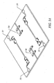
- Fig. 2 is a plan view of the circuitry of Fig. 1 realized using a coplanar coupler in accordance with the present invention. In this view, all metal traces and circuitry are on the top surface of the substrate except for the couplers 14 and 16 which are on the bottom surface.
- Input port 10 and isolation port 11 comprise metalization on the top surface which cooperates with a metalized layer on the bottom surface to form a microstrip input line.
- output port 20 and an isolation port 21 comprise metalization on the top surface which cooperates with the metalization on the bottom surface as a microstrip output line.
- the coplanar couplers 14,16 comprise metalization on the bottom surface formed in areas 24, 26 where the backside metalization has been removed.
- Planar coupler 14 comprises interdigitated U-shaped metal traces 31, 32 with metal trace 31 connected by throughhole vias 33 to input metalization 10 and to metal trace 34 through via 35.
- U-shaped metal trace 32 is connected to isolation port 11 through vias 36 and to microstrip trace 38 through via 39.
- Coupler 16 has similar structure as coupler 14 with the U-shaped metal traces on the bottom surface connected to microstrip 40 and 42, and to output port 20 and isolation port 21 by conductive vias through the substrate.
- a bias voltage (at RF ground) can be connected by microstrip 44 on the top surface over and spaced from coupler 14 on the bottom surface, providing a bias voltage to circuitry shown generally at 50.
- the bias voltage line 44 is coupled to the ground layer on the bottom surface through capacitors 46 and vias 48.
- the cross-over structure allows DC bias to be taken at right angles to the coplanar coupler lines and cross over the coupler lines without degrading the performance of the coplanar coupler while maintaining a high degree of electrical isolation between the coupler and the DC track.
- the inverted coplanar coupler can have a center section under the DC bias cross-over which functions as a part grounded coplanar waveguide. By adjusting the amount of the grounded coplanar waveguide center section, the characteristics of the overall coupler can be optimized.
- Fig. 3A illustrates the metal traces on a portion of the top surface of the substrate including input port and microstrip 10, isolation port and microstrip 11, amplifiers 54, 56, the output microstrip port 20 and output isolation port 21.
- Fig. 3B is a plan view of the bottom surface showing the metal layer 50 with a removed portion 24 in which is formed the coplanar coupler 14.
- Fig. 4 shows a three dimensional view of representative vias 48 and their role in interconnecting the top microstrip trace to the bottom coplanar waveguide traces.
- these same improved coplanar couplers can be combined with mixers and modulators to form quadrature-balanced mixers and modulators.
- a single improved coplanar coupler can be applied in conjunction with an in-phase divider/combiner to form IQ modulators and image reject mixers.
Abstract
Description
- This invention relates generally to microwave circuits, and more particularly the invention relates to signal couplers as used in microwave circuits. Microwave circuits often use signal couplers between circuit sections. Numerous coupling structures have been used in the past, including microstrip coupled lines, stripline coupled lines, and coplanar waveguide coupled lines. The most common form of microwave circuitry is microstrip transmission lines. Microstrip couplers, such as the Lange coupler, are difficult to manufacture in printed circuit boards which have limited and rather course resolution of lines and spaces. This is particularly true when one requires high coupling values on the order of -3 dB (i.e., one-half of the incident energy). It has been demonstrated previously that a coplanar waveguide coupler can satisfy the high value coupling while only requiring medium resolution of line widths and gaps. However, a coupler realized entirely in coplanar waveguide form requires microstrip-to-coplanar waveguide transitions which consume space and place restrictions on circuit design.
-
Frick U.S. Patent No. 5,629,654 discloses a totally coplanar waveguide construction. However, for many applications it is desirable to have microstrip transmission line input and output ports. Prior art designs require separate microstrip-to-coplanar transitions in order to use a coplanar waveguide coupler with microstrip input and output ports. This adds complexity to circuit design and consumes additional circuit board space. - The present invention is directed to providing a coplanar coupler for microstrip input/output ports which is space efficient and compatible with printed circuit board manufacturing considerations while providing requisite coupling value, terminal return loss, and isolation.
-
US Patent No. 4,675,620 discloses a crossover for coplanar waveguides in which a pair of microstrip/strip line conductors on one side of the substrate are transitioned into coplanar conductors on opposite sides of the substrate. - In accordance with the invention, there is provided a method for producing a microwave circuit having a coplanar waveguide coupler according to claim 7 and a coplanar waveguide coupler according to claim 1. A coupler for microstrip input and output ports in a microwave circuit may be fabricated on a printed circuit substrate in which the microstrip input and output lines are on one surface of the substrate, and the coplanar coupler lines are on an opposite surface of the substrate with vias interconnecting the microstrip ports with the coplanar coupler lines.
- A metal layer is formed on the surface with the coplanar coupler, but is spaced from the coupler. The metal layer functions with the input and output ports in forming the microstrip ground plane.
- In an example, first and second metal lines of the coplanar coupler are in spaced parallel alignment, and preferably comprise U-shaped metal traces. A bias metal line can be placed on the surface with the input and output ports which extends across and spaced from the coplanar coupler lines on the opposing surface for providing bias voltage to circuit components mounted on the surface. By grounding the bias metal line, the coplanar coupler can include a partial grounded coplanar waveguide. The amount of the grounded coplanar waveguide center region can be adjusted to optimize the characteristics of the overall coupler.
- The structure in accordance with the invention is efficient in substrate space which results in cost, manufacturing, and application enhancements. The invention and objects and features thereof will be more readily apparent from the following detailed description and appended claims when taken with the drawings.
-
-
Fig. 1 is a functional block diagram of a quadrature balanced amplifier module in which couplers in accordance with the invention can be employed. -
Fig. 2 is a top view illustrating metal traces on top and bottom surfaces of a printed circuit substrate for a coplanar coupler in accordance with the invention. -
Fig. 3A is a plan view of metalization for the input and output ports on one surface of the structure ofFig. 2 , andFig. 3B is a plan view of metalization for the coplanar coupler on the bottom surface of the structure ofFig. 2 . -
Fig. 4 is a three dimensional view of the metal traces on the top and bottom surfaces and the interconnecting vias. -
Fig. 1 is a functional block diagram of a microwave circuit in which an input signal at 10 is applied through acoupler 12 toquadrature balance amplifiers coupler 18 to anoutput 20. Typically, theinput line 10 andoutput line 20 are microstrip comprising a metal trace on one surface of a substrate over a grounded metal layer on the opposing surface of the substrate, andcouplers Frick U.S. Patent No. 5,629,654 discloses input and output microstrip withcoplanar coupler 12 all formed on one surface of the printed circuit of the substrate. As noted above, this arrangement is not cost or space effective. - In accordance with the present invention, improved cost and performance are realized by placing the microstrip input and output lines on one surface of the substrate and placing the coplanar coupler lines on another surface of the substrate with the input and output lines connected to the coplanar coupler by feedthrough vias through the substrate. The substrate can be ceramic with gold, silver, or copper metal lines, or other suitable substrates and metal layers can be used.
Fig. 2 is a plan view of the circuitry ofFig. 1 realized using a coplanar coupler in accordance with the present invention. In this view, all metal traces and circuitry are on the top surface of the substrate except for thecouplers Input port 10 andisolation port 11 comprise metalization on the top surface which cooperates with a metalized layer on the bottom surface to form a microstrip input line. Similarly,output port 20 and anisolation port 21 comprise metalization on the top surface which cooperates with the metalization on the bottom surface as a microstrip output line. Thecoplanar couplers areas Planar coupler 14 comprises interdigitated U-shapedmetal traces metal trace 31 connected bythroughhole vias 33 toinput metalization 10 and tometal trace 34 through via 35. Similarly, U-shapedmetal trace 32 is connected toisolation port 11 throughvias 36 and tomicrostrip trace 38 through via 39. Closely spacedparallel lines amplifiers microstrip output amplifiers coupler 16 on the bottom surface.Coupler 16 has similar structure ascoupler 14 with the U-shaped metal traces on the bottom surface connected tomicrostrip port 20 andisolation port 21 by conductive vias through the substrate. - In accordance with a feature of the invention, a bias voltage (at RF ground) can be connected by
microstrip 44 on the top surface over and spaced fromcoupler 14 on the bottom surface, providing a bias voltage to circuitry shown generally at 50. Thebias voltage line 44 is coupled to the ground layer on the bottom surface throughcapacitors 46 andvias 48. The cross-over structure allows DC bias to be taken at right angles to the coplanar coupler lines and cross over the coupler lines without degrading the performance of the coplanar coupler while maintaining a high degree of electrical isolation between the coupler and the DC track. The inverted coplanar coupler can have a center section under the DC bias cross-over which functions as a part grounded coplanar waveguide. By adjusting the amount of the grounded coplanar waveguide center section, the characteristics of the overall coupler can be optimized. -
Fig. 3A illustrates the metal traces on a portion of the top surface of the substrate including input port andmicrostrip 10, isolation port andmicrostrip 11,amplifiers output microstrip port 20 andoutput isolation port 21.Fig. 3B is a plan view of the bottom surface showing the metal layer 50 with a removedportion 24 in which is formed thecoplanar coupler 14.Fig. 4 shows a three dimensional view ofrepresentative vias 48 and their role in interconnecting the top microstrip trace to the bottom coplanar waveguide traces. For example, these same improved coplanar couplers can be combined with mixers and modulators to form quadrature-balanced mixers and modulators. A single improved coplanar coupler can be applied in conjunction with an in-phase divider/combiner to form IQ modulators and image reject mixers.
Claims (8)
- A microwave circuit comprising:a) a printed circuit substrate having a first surface and a second opposite the first surface of the substrate, with circuity (50) on the second surface,b) first and second metal microstrip input ports (10,11) formed on the first surface,c) first and second metal microstrip output ports (34,38) formed on the first surface,d) a metal layer on the second surface functioning as a ground plane for the input ports and the output ports as microstrip,e) a coplanar waveguide coupler (14,16) for the input port and output port formed on the second surface, comprising first and second metal lines (31, 32), the metal layer covering the second surface except in a coplanar waveguide coupler region under at least portions of the metal input and output parts and extending there betweenf) a bias voltage metal line (44) for the circuitry on the first surface extending across at right angles and spaced from a center section the first and second metal lines (31, 32) of the coplanar waveguide coupler, the bias voltage metal the being coupled to the metal layer on the second surface through capacitors (46) andg) electrical connectors (33,35,36,39) connecting one input port and one output port to the first metal line and connecting the other input port and the other output port to the second metal line.
- The microwave circuit of Claim 1, wherein the first and second metal lines of the coplanar waveguide coupler comprise first and second interdigitated U-shaped metal lines (31,32) on the bottom surface in the coupler region.
- The microwave circuit defined by Claim 2 wherein the first and second metal lines (31,32) are in spaced parallel arrangement.
- The microwave circuit defined by Claim 2 or Claim 3 wherein the electrical connectors are feedthrough vias in the substrate.
- The microwave circuit as defined by Claim 4 wherein the substrate is ceramic.
- The microwave circuit as defined by Claim 5 wherein the metal is selected from the group consisting of gold, silver, and copper.
- A method for producing the microwave circuit of claim 1 having a coplanar waveguide coupler (14,16) for microstrip input and 5 output lines on a printed circuit substrate, the method comprising:a) placing microstrip input (10,11) and output (34, 38) parts on a first surface of the substrate,b) placing coplanar waveguide coupler lines (31,32) and a ground conductor on a second surface of the substrate, opposite the first surface of the substrate, the ground conductor being a metal layer covering the second surface except in a coplanar waveguide coupler region under out least portions of the metal input and aspect parts and extending therebetween,c) interconnecting the microstrip input and output parts on the first surface to the coplanar waveguide coupler lines on the second surface, andd) placing circuitry (50) on the second surface of the substrate,e) providing a bias metal line (44) for the circuitry on the first surface extending across at right angles and spaced from a center section of the first and second metal lines (31,32) of the coplanar coupler the bias voltage metal line being coupled to the metal layer on the second surface through capacitors (46).
- The method as defined by Claim 7 wherein the step of c) includes the use of feedthrough vias (33,35,36,39) and
Applications Claiming Priority (3)
| Application Number | Priority Date | Filing Date | Title |
|---|---|---|---|
| US910311 | 2001-07-19 | ||
| US09/910,311 US6549090B2 (en) | 2001-07-19 | 2001-07-19 | Inverted coplanar waveguide coupler with integral microstrip connection ports |
| PCT/US2002/023045 WO2003009414A1 (en) | 2001-07-19 | 2002-07-18 | Inverted coplanar waveguide coupler with integral microstrip connection ports |
Publications (3)
| Publication Number | Publication Date |
|---|---|
| EP1433220A1 EP1433220A1 (en) | 2004-06-30 |
| EP1433220A4 EP1433220A4 (en) | 2005-03-30 |
| EP1433220B1 true EP1433220B1 (en) | 2011-12-14 |
Family
ID=25428603
Family Applications (1)
| Application Number | Title | Priority Date | Filing Date |
|---|---|---|---|
| EP02750194A Expired - Lifetime EP1433220B1 (en) | 2001-07-19 | 2002-07-18 | Inverted coplanar waveguide coupler with integral microstrip connection ports |
Country Status (9)
| Country | Link |
|---|---|
| US (1) | US6549090B2 (en) |
| EP (1) | EP1433220B1 (en) |
| JP (1) | JP4145241B2 (en) |
| KR (1) | KR20040018411A (en) |
| CN (1) | CN100521366C (en) |
| AT (1) | ATE537577T1 (en) |
| CA (1) | CA2454131A1 (en) |
| TW (1) | TW586252B (en) |
| WO (1) | WO2003009414A1 (en) |
Families Citing this family (12)
| Publication number | Priority date | Publication date | Assignee | Title |
|---|---|---|---|---|
| US8143108B2 (en) | 2004-10-07 | 2012-03-27 | Stats Chippac, Ltd. | Semiconductor device and method of dissipating heat from thin package-on-package mounted to substrate |
| US20020121707A1 (en) * | 2001-02-27 | 2002-09-05 | Chippac, Inc. | Super-thin high speed flip chip package |
| DE10316047B4 (en) | 2003-04-08 | 2006-11-30 | Rohde & Schwarz Gmbh & Co. Kg | Directional coupler in coplanar waveguide technology |
| US7123883B2 (en) * | 2003-09-26 | 2006-10-17 | Nokia Corporation | Systems and methods that employ a balanced duplexer |
| US20060019611A1 (en) * | 2004-07-21 | 2006-01-26 | Nokia Corporation | Distributed balanced duplexer |
| DE102007029125A1 (en) | 2007-06-25 | 2009-01-02 | Rohde & Schwarz Gmbh & Co. Kg | Broadband directional coupler with adjustable directivity |
| CN101728620B (en) * | 2010-01-28 | 2013-02-13 | 大连海事大学 | Asymmetric coplanar waveguide directional coupler |
| TWI395519B (en) * | 2010-06-28 | 2013-05-01 | Wistron Neweb Corp | Circuit board with jumper structure |
| US8878627B2 (en) * | 2011-04-29 | 2014-11-04 | Cyntec Co., Ltd. | Monolithic power splitter for differential signal |
| US9212942B2 (en) * | 2012-07-04 | 2015-12-15 | Vega Grieshaber Kg | Waveguide coupling, high-frequency module, fill-level radar and use |
| US10429582B1 (en) * | 2018-05-02 | 2019-10-01 | Globalfoundries Inc. | Waveguide-to-waveguide couplers with multiple tapers |
| CN113708038B (en) * | 2021-08-23 | 2022-07-15 | 南京邮电大学 | High-isolation radio frequency filtering power divider |
Family Cites Families (11)
| Publication number | Priority date | Publication date | Assignee | Title |
|---|---|---|---|---|
| US4118670A (en) * | 1975-05-08 | 1978-10-03 | Westinghouse Electric Corp. | Image phased and idler frequency controlled mixer formed on an integrated circuit dielectric substrate |
| US4482873A (en) | 1982-09-16 | 1984-11-13 | Rockwell International Corporation | Printed hybrid quadrature 3 dB signal coupler apparatus |
| US4591812A (en) | 1982-11-22 | 1986-05-27 | Communications Satellite Corporation | Coplanar waveguide quadrature hybrid having symmetrical coupling conductors for eliminating spurious modes |
| US4675620A (en) | 1986-03-03 | 1987-06-23 | Motorola, Inc. | Coplanar waveguide crossover |
| US5105171A (en) | 1991-04-29 | 1992-04-14 | Hughes Aircraft Company | Coplanar waveguide directional coupler and flip-clip microwave monolithic integrated circuit assembly incorporating the coupler |
| JP3168658B2 (en) * | 1992-01-16 | 2001-05-21 | 株式会社村田製作所 | Directional coupler |
| JP2651336B2 (en) * | 1993-06-07 | 1997-09-10 | 株式会社エイ・ティ・アール光電波通信研究所 | Directional coupler |
| US5629654A (en) | 1996-05-06 | 1997-05-13 | Watkins-Johnson Company | Coplanar waveguide coupler |
| US6263198B1 (en) * | 1996-06-14 | 2001-07-17 | Wj Communications, Inc. | Multi-layer printed wiring board having integrated broadside microwave coupled baluns |
| US6204736B1 (en) * | 1998-11-25 | 2001-03-20 | Merrimac Industries, Inc. | Microwave mixer with baluns having rectangular coaxial transmission lines |
| US6294965B1 (en) * | 1999-03-11 | 2001-09-25 | Anaren Microwave, Inc. | Stripline balun |
-
2001
- 2001-07-19 US US09/910,311 patent/US6549090B2/en not_active Expired - Lifetime
-
2002
- 2002-07-18 KR KR10-2003-7017278A patent/KR20040018411A/en not_active Application Discontinuation
- 2002-07-18 CA CA002454131A patent/CA2454131A1/en not_active Abandoned
- 2002-07-18 JP JP2003514649A patent/JP4145241B2/en not_active Expired - Lifetime
- 2002-07-18 CN CNB028145895A patent/CN100521366C/en not_active Expired - Lifetime
- 2002-07-18 EP EP02750194A patent/EP1433220B1/en not_active Expired - Lifetime
- 2002-07-18 AT AT02750194T patent/ATE537577T1/en active
- 2002-07-18 WO PCT/US2002/023045 patent/WO2003009414A1/en active Application Filing
- 2002-07-19 TW TW091116141A patent/TW586252B/en not_active IP Right Cessation
Also Published As
| Publication number | Publication date |
|---|---|
| US20030016095A1 (en) | 2003-01-23 |
| WO2003009414A1 (en) | 2003-01-30 |
| EP1433220A4 (en) | 2005-03-30 |
| TW586252B (en) | 2004-05-01 |
| JP2004522378A (en) | 2004-07-22 |
| EP1433220A1 (en) | 2004-06-30 |
| CN1533623A (en) | 2004-09-29 |
| CA2454131A1 (en) | 2003-01-30 |
| CN100521366C (en) | 2009-07-29 |
| US6549090B2 (en) | 2003-04-15 |
| JP4145241B2 (en) | 2008-09-03 |
| KR20040018411A (en) | 2004-03-03 |
| ATE537577T1 (en) | 2011-12-15 |
Similar Documents
| Publication | Publication Date | Title |
|---|---|---|
| US7319370B2 (en) | 180 degrees hybrid coupler | |
| US6201439B1 (en) | Power splitter/ combiner circuit, high power amplifier and balun circuit | |
| EP0511728B1 (en) | Coplanar waveguide directional coupler and flip-chip microwave monolithic integrated circuit assembly incorporating the coupler | |
| US7009467B2 (en) | Directional coupler | |
| EP1433220B1 (en) | Inverted coplanar waveguide coupler with integral microstrip connection ports | |
| EP1366539B1 (en) | Coupling device using buried capacitors in multilayered substrate | |
| EP1208615B1 (en) | Four port hybrid | |
| US5629654A (en) | Coplanar waveguide coupler | |
| EP1346432B1 (en) | Four port hybrid microstrip circuit of lange type | |
| US6946927B2 (en) | Suspended substrate low loss coupler | |
| EP0774171B1 (en) | Bypassable power divider/combiner | |
| US20230034066A1 (en) | BROADBAND AND LOW COST PRINTED CIRCUIT BOARD BASED 180º HYBRID COUPLERS ON A SINGLE LAYER BOARD | |
| US20090284326A1 (en) | Balanced hybrid coupler | |
| JPH01231501A (en) | 180-degree hybrid | |
| JPH06177617A (en) | Wide-band directional coupler | |
| JPH03258003A (en) | Microwave ceramic module |
Legal Events
| Date | Code | Title | Description |
|---|---|---|---|
| PUAI | Public reference made under article 153(3) epc to a published international application that has entered the european phase |
Free format text: ORIGINAL CODE: 0009012 |
|
| 17P | Request for examination filed |
Effective date: 20040213 |
|
| AK | Designated contracting states |
Kind code of ref document: A1 Designated state(s): AT BE BG CH CY CZ DE DK EE ES FI FR GB GR IE IT LI LU MC NL PT SE SK TR |
|
| AX | Request for extension of the european patent |
Extension state: AL LT LV MK RO SI |
|
| A4 | Supplementary search report drawn up and despatched |
Effective date: 20050215 |
|
| RIC1 | Information provided on ipc code assigned before grant |
Ipc: 7H 01P 5/18 A Ipc: 7H 01P 5/08 B |
|
| RAP1 | Party data changed (applicant data changed or rights of an application transferred) |
Owner name: CREE MICROWAVE, LLC |
|
| 17Q | First examination report despatched |
Effective date: 20070307 |
|
| RAP1 | Party data changed (applicant data changed or rights of an application transferred) |
Owner name: CREE, INC. |
|
| GRAP | Despatch of communication of intention to grant a patent |
Free format text: ORIGINAL CODE: EPIDOSNIGR1 |
|
| GRAS | Grant fee paid |
Free format text: ORIGINAL CODE: EPIDOSNIGR3 |
|
| GRAA | (expected) grant |
Free format text: ORIGINAL CODE: 0009210 |
|
| AK | Designated contracting states |
Kind code of ref document: B1 Designated state(s): AT BE BG CH CY CZ DE DK EE ES FI FR GB GR IE IT LI LU MC NL PT SE SK TR |
|
| REG | Reference to a national code |
Ref country code: GB Ref legal event code: FG4D |
|
| REG | Reference to a national code |
Ref country code: CH Ref legal event code: EP |
|
| REG | Reference to a national code |
Ref country code: IE Ref legal event code: FG4D |
|
| REG | Reference to a national code |
Ref country code: DE Ref legal event code: R096 Ref document number: 60241744 Country of ref document: DE Effective date: 20120301 |
|
| REG | Reference to a national code |
Ref country code: NL Ref legal event code: VDEP Effective date: 20111214 |
|
| PG25 | Lapsed in a contracting state [announced via postgrant information from national office to epo] |
Ref country code: SE Free format text: LAPSE BECAUSE OF FAILURE TO SUBMIT A TRANSLATION OF THE DESCRIPTION OR TO PAY THE FEE WITHIN THE PRESCRIBED TIME-LIMIT Effective date: 20111214 Ref country code: NL Free format text: LAPSE BECAUSE OF FAILURE TO SUBMIT A TRANSLATION OF THE DESCRIPTION OR TO PAY THE FEE WITHIN THE PRESCRIBED TIME-LIMIT Effective date: 20111214 Ref country code: GR Free format text: LAPSE BECAUSE OF FAILURE TO SUBMIT A TRANSLATION OF THE DESCRIPTION OR TO PAY THE FEE WITHIN THE PRESCRIBED TIME-LIMIT Effective date: 20120315 |
|
| PG25 | Lapsed in a contracting state [announced via postgrant information from national office to epo] |
Ref country code: CY Free format text: LAPSE BECAUSE OF FAILURE TO SUBMIT A TRANSLATION OF THE DESCRIPTION OR TO PAY THE FEE WITHIN THE PRESCRIBED TIME-LIMIT Effective date: 20111214 Ref country code: BE Free format text: LAPSE BECAUSE OF FAILURE TO SUBMIT A TRANSLATION OF THE DESCRIPTION OR TO PAY THE FEE WITHIN THE PRESCRIBED TIME-LIMIT Effective date: 20111214 |
|
| PG25 | Lapsed in a contracting state [announced via postgrant information from national office to epo] |
Ref country code: CZ Free format text: LAPSE BECAUSE OF FAILURE TO SUBMIT A TRANSLATION OF THE DESCRIPTION OR TO PAY THE FEE WITHIN THE PRESCRIBED TIME-LIMIT Effective date: 20111214 Ref country code: EE Free format text: LAPSE BECAUSE OF FAILURE TO SUBMIT A TRANSLATION OF THE DESCRIPTION OR TO PAY THE FEE WITHIN THE PRESCRIBED TIME-LIMIT Effective date: 20111214 Ref country code: BG Free format text: LAPSE BECAUSE OF FAILURE TO SUBMIT A TRANSLATION OF THE DESCRIPTION OR TO PAY THE FEE WITHIN THE PRESCRIBED TIME-LIMIT Effective date: 20120314 Ref country code: SK Free format text: LAPSE BECAUSE OF FAILURE TO SUBMIT A TRANSLATION OF THE DESCRIPTION OR TO PAY THE FEE WITHIN THE PRESCRIBED TIME-LIMIT Effective date: 20111214 |
|
| PG25 | Lapsed in a contracting state [announced via postgrant information from national office to epo] |
Ref country code: PT Free format text: LAPSE BECAUSE OF FAILURE TO SUBMIT A TRANSLATION OF THE DESCRIPTION OR TO PAY THE FEE WITHIN THE PRESCRIBED TIME-LIMIT Effective date: 20120416 |
|
| REG | Reference to a national code |
Ref country code: AT Ref legal event code: MK05 Ref document number: 537577 Country of ref document: AT Kind code of ref document: T Effective date: 20111214 |
|
| PLBE | No opposition filed within time limit |
Free format text: ORIGINAL CODE: 0009261 |
|
| STAA | Information on the status of an ep patent application or granted ep patent |
Free format text: STATUS: NO OPPOSITION FILED WITHIN TIME LIMIT |
|
| PG25 | Lapsed in a contracting state [announced via postgrant information from national office to epo] |
Ref country code: DK Free format text: LAPSE BECAUSE OF FAILURE TO SUBMIT A TRANSLATION OF THE DESCRIPTION OR TO PAY THE FEE WITHIN THE PRESCRIBED TIME-LIMIT Effective date: 20111214 |
|
| 26N | No opposition filed |
Effective date: 20120917 |
|
| PG25 | Lapsed in a contracting state [announced via postgrant information from national office to epo] |
Ref country code: IT Free format text: LAPSE BECAUSE OF FAILURE TO SUBMIT A TRANSLATION OF THE DESCRIPTION OR TO PAY THE FEE WITHIN THE PRESCRIBED TIME-LIMIT Effective date: 20111214 |
|
| REG | Reference to a national code |
Ref country code: DE Ref legal event code: R097 Ref document number: 60241744 Country of ref document: DE Effective date: 20120917 |
|
| PG25 | Lapsed in a contracting state [announced via postgrant information from national office to epo] |
Ref country code: AT Free format text: LAPSE BECAUSE OF FAILURE TO SUBMIT A TRANSLATION OF THE DESCRIPTION OR TO PAY THE FEE WITHIN THE PRESCRIBED TIME-LIMIT Effective date: 20111214 |
|
| PG25 | Lapsed in a contracting state [announced via postgrant information from national office to epo] |
Ref country code: MC Free format text: LAPSE BECAUSE OF NON-PAYMENT OF DUE FEES Effective date: 20120731 |
|
| REG | Reference to a national code |
Ref country code: CH Ref legal event code: PL |
|
| PG25 | Lapsed in a contracting state [announced via postgrant information from national office to epo] |
Ref country code: CH Free format text: LAPSE BECAUSE OF NON-PAYMENT OF DUE FEES Effective date: 20120731 Ref country code: ES Free format text: LAPSE BECAUSE OF FAILURE TO SUBMIT A TRANSLATION OF THE DESCRIPTION OR TO PAY THE FEE WITHIN THE PRESCRIBED TIME-LIMIT Effective date: 20120325 Ref country code: LI Free format text: LAPSE BECAUSE OF NON-PAYMENT OF DUE FEES Effective date: 20120731 |
|
| REG | Reference to a national code |
Ref country code: IE Ref legal event code: MM4A |
|
| PG25 | Lapsed in a contracting state [announced via postgrant information from national office to epo] |
Ref country code: FI Free format text: LAPSE BECAUSE OF FAILURE TO SUBMIT A TRANSLATION OF THE DESCRIPTION OR TO PAY THE FEE WITHIN THE PRESCRIBED TIME-LIMIT Effective date: 20111214 |
|
| PG25 | Lapsed in a contracting state [announced via postgrant information from national office to epo] |
Ref country code: IE Free format text: LAPSE BECAUSE OF NON-PAYMENT OF DUE FEES Effective date: 20120718 |
|
| PG25 | Lapsed in a contracting state [announced via postgrant information from national office to epo] |
Ref country code: TR Free format text: LAPSE BECAUSE OF FAILURE TO SUBMIT A TRANSLATION OF THE DESCRIPTION OR TO PAY THE FEE WITHIN THE PRESCRIBED TIME-LIMIT Effective date: 20111214 |
|
| PG25 | Lapsed in a contracting state [announced via postgrant information from national office to epo] |
Ref country code: LU Free format text: LAPSE BECAUSE OF NON-PAYMENT OF DUE FEES Effective date: 20120718 |
|
| REG | Reference to a national code |
Ref country code: FR Ref legal event code: PLFP Year of fee payment: 15 |
|
| REG | Reference to a national code |
Ref country code: FR Ref legal event code: PLFP Year of fee payment: 16 |
|
| REG | Reference to a national code |
Ref country code: FR Ref legal event code: PLFP Year of fee payment: 17 |
|
| PGFP | Annual fee paid to national office [announced via postgrant information from national office to epo] |
Ref country code: FR Payment date: 20210726 Year of fee payment: 20 |
|
| PGFP | Annual fee paid to national office [announced via postgrant information from national office to epo] |
Ref country code: DE Payment date: 20210728 Year of fee payment: 20 Ref country code: GB Payment date: 20210727 Year of fee payment: 20 |
|
| REG | Reference to a national code |
Ref country code: DE Ref legal event code: R071 Ref document number: 60241744 Country of ref document: DE |
|
| REG | Reference to a national code |
Ref country code: GB Ref legal event code: PE20 Expiry date: 20220717 |
|
| PG25 | Lapsed in a contracting state [announced via postgrant information from national office to epo] |
Ref country code: GB Free format text: LAPSE BECAUSE OF EXPIRATION OF PROTECTION Effective date: 20220717 |