EP1433218B1 - A tunable ferroelectric resonator arrangement - Google Patents
A tunable ferroelectric resonator arrangement Download PDFInfo
- Publication number
- EP1433218B1 EP1433218B1 EP02759031A EP02759031A EP1433218B1 EP 1433218 B1 EP1433218 B1 EP 1433218B1 EP 02759031 A EP02759031 A EP 02759031A EP 02759031 A EP02759031 A EP 02759031A EP 1433218 B1 EP1433218 B1 EP 1433218B1
- Authority
- EP
- European Patent Office
- Prior art keywords
- resonator
- tunable
- resonators
- electrode plate
- substrate
- Prior art date
- Legal status (The legal status is an assumption and is not a legal conclusion. Google has not performed a legal analysis and makes no representation as to the accuracy of the status listed.)
- Expired - Lifetime
Links
Images


Classifications
-
- H—ELECTRICITY
- H01—ELECTRIC ELEMENTS
- H01P—WAVEGUIDES; RESONATORS, LINES, OR OTHER DEVICES OF THE WAVEGUIDE TYPE
- H01P7/00—Resonators of the waveguide type
- H01P7/10—Dielectric resonators
-
- H—ELECTRICITY
- H01—ELECTRIC ELEMENTS
- H01P—WAVEGUIDES; RESONATORS, LINES, OR OTHER DEVICES OF THE WAVEGUIDE TYPE
- H01P1/00—Auxiliary devices
- H01P1/20—Frequency-selective devices, e.g. filters
-
- H—ELECTRICITY
- H01—ELECTRIC ELEMENTS
- H01P—WAVEGUIDES; RESONATORS, LINES, OR OTHER DEVICES OF THE WAVEGUIDE TYPE
- H01P1/00—Auxiliary devices
- H01P1/20—Frequency-selective devices, e.g. filters
- H01P1/201—Filters for transverse electromagnetic waves
- H01P1/203—Strip line filters
Definitions
- the present invention relates to a tunable resonating arrangement which comprises a resonator apparatus. Electromagnetic energy is coupled into/out of the resonator apparatus over input/output coupling means, and for tuning of the resonator apparatus, a tuning device is used for application of a biasing/tuning voltage (electric field) to the resonator apparatus.
- the resonator apparatus comprises a first non-tunable resonator and a second resonator, which is tunable and comprises a ferroelectric substrate.
- Coupling means are provided for coupling between the first and second resonators, which are separated by a ground plane common for the first and second resonators.
- the invention also relates to a method of tuning a resonating arrangement.
- Electrically tunable resonators are attractive components for agile radar and mobile radio communication systems. Different types of resonators are known. Dielectric and parallel plate resonator and filters for microwave frequencies using dielectric disks of any shape, for example circular, are known e.g. from Vendik et al., Electronics Letters vol. 31, p. 654, 1995 .
- Parallel plate resonators comprising substrates of non-linear dielectric materials with extremely high dielectric constants, for example ferroelectric materials or anti-ferroelectric materials, have small dimensions, and they can for example be used to provide very compact filters in the frequency bands in which advanced microwave communication systems operate.
- non-linear dielectric materials may e.g. be STO(SrTiO 3 ) with a dielectric constant of about 2000 at the temperature of liquid nitrogen and a dielectric constant of about 300 at room temperature.
- Dielectric, parallel plate resonators can be excited by simple probes or loops.
- the thickness of a parallel plate resonator is much smaller than the wavelength of the microwave signal in the resonator in order for the resonator to support only the lowest order TM modes and in order to keep the DC-voltages, which are required for the electrical tuning of the resonator comprising a dielectric substrate with electrodes arranged on both sides of it, as low as possible.
- electrical tuning is obtained by means of the application of an external DC-biasing voltage, which is supplied by means of ohmic contacts to the electrodes acting as plates of the resonator.
- Tunable resonators based on thin film substrates as well as resonators based on dielectric bulk substrates are known.
- a resonator is considered to be electrically thin if the thickness is smaller than half the wavelength of the microwave signal in the resonator such that no standing waves will be present along the axis of the disk.
- Electrically tunable resonators based on circular ferroelectric disks have recently been found attractive and have drawn much attention for example for applications as tunable filters in microwave communication systems, as well as in mobile radio communication systems.
- Such devices are for example described in "Tunable Microwave Devices", which is a Swedish patent application with application number 9502137-4 and "Arrangement and method relating to tunable devices” which is a Swedish patent application with application number 9502138-2 .
- ferroelectric materials are able to handle high peak power, they have a low switching time, and the dielectric constant of the substrate varies with an applied biasing voltage, which makes the impedance of the device vary with an applied biasing electric field.
- US-A-5 908 811 "High Tc Superconducting Ferroelectric Tunable Filters” shows an example of such a filter which should get low losses by means of using a single crystal ferroelectric material.
- a ferroelectric thin film substrate is used.
- US-A-5 935 910 shows an example of a high power band-pass filter which is made of two waveguide cavities (resonators) limited by respective irises. Both cavities are tunable and comprise hollow waveguides loaded by ferroelectric rings. Electrodes of the rings are formed on the inside and outside of cylindrical surfaces and the rings are used to perturb or tune the hollow cavities (resonators) between the irises.
- a tunable resonating arrangement more particularly for microwaves or millimeter waves, which has small dimensions and which can be used in different kinds of advanced microwave communication systems and mobile radio communication systems.
- a tunable resonator arrangement is also needed which has a high, or at least satisfactory, performance, and which is easy to fabricate.
- a tunable resonating arrangement is needed through which it is possible to compensate for the losses in a ferroelectric substrate upon application of an electric field/voltage for tuning purposes.
- Particularly an arrangement is needed which has a high power handling capability. Even more particularly an arrangement is needed through which tuning by the means of the application of a DC-biasing can be provided substantially without deteriorating. the quality factor (Q-value) of the resonator.
- An arrangement is also needed which is compact in size for use in different types of components, which can be tuned efficiently without requiring too high amounts of power, and which is reliable in operation. Moreover an arrangement is needed which is robust and which has a satisfactory tuning selectivity and tuning sensitivity, and through which the insertion losses are low or can be compensated for.
- a tunable filter arrangement is also needed which comprises one a more resonator apparatuses and which meets one or more of the objects referred to above. Still further a method of tuning a resonator arrangement is needed through which the above mentioned objects can be achieved, and particularly a method of compensating for the losses induced in a ferroelectric resonator substrate through electrical or electronical tuning.
- the first resonator is a parallel plate resonator which comprises a dielectric bulk or thin film disk substrate with a first electrode plate disposed on one side of the dielectric substrate and a second electrode plate disposed on the other side of the dielectric substrate, the electric permittivity of which substantially does not vary with applied biasing voltage.
- the second resonator comprises a tunable ferroelectric substrate bulk or thin film disk substrate with a first electrode plate disposed on one side of the ferroelectric substrate and a second electrode plate disposed on the other side of the ferroelectric substrate.
- the second electrode plate of the second resonator is the same as the second electrode plate of the first resonator and forms the said common ground plane.
- the biasing voltage/electric field is applied to the second resonator.
- the dielectric substrate of the first resonator may for example comprised LaAlO 3 , MgO, NdGaO 3 Al 2 O 3 , sapphire or a material with similar properties.
- the quality factor (Q-value) of the first resonator may exceed approximately 10 5 -5 ⁇ 10 5 .
- the substrate of the second resonator may for example comprise SrTiO 3 , KTaO 3 , or BaSTO 3 or any other material with similar properties.
- the first and second electrodes of each resonator which here means the first electrodes and the common ground plane, in one implementation consist of normal conducting metal, such as for example Au, Ag, Cu.
- the first and second electrodes i.e. the first electrodes and the common ground plane, consist of a superconducting material.
- the first and second electrodes i.e. the first electrodes and the common ground plane, consist of a high temperature superconducting material (HTS), for example YBCO (Y-Ba-Cu-O).
- HTS high temperature superconducting material
- YBCO Y-Ba-Cu-O
- Other alternatives are TBCCO and BSCCO.
- superconductors or superconducting films are used, which may be covered by thin non-superconducting high conductivity films of for example Au, Ag, Cu or similar.
- Such devices are also discussed in "Tunable Microwave Devices" referred to above.
- the first and second resonators are TM020 mode resonators.
- other modes can be selected, as discussed example in the Swedish patent application “Microwave Devices and Method Relating Thereto" with application number 9901190-0 which illustrates how different modes can be selected, and which gives example on which mode(s) that can be selected, for exemplifying reasons.
- the first and second resonators comprise disk resonators based on a dielectric/ferroelectric bulk material. They may however also comprise thin film substrates. However, by using tunable disk resonators resonating arrangements, particularly filters, which have a much higher power handling capability than those made of tunable thin film, can be realized.
- the resonating arrangement comprises at least two resonator apparatuses, and the common ground plane is common for (shared by) the at least two resonator apparatuses to form a tunable filter.
- the coupling means may comprise, for each resonator apparatus, a slot or an aperture in the common ground plane.
- the resonators may be of substantially any appropriate shape, they may e.g. be circular, square-shaped, rectangular or ellipsoidal etc.
- the shape of the first resonator may also differ from that of the second resonator.
- the resonator apparatus may also be a dual mode resonator apparatus.
- each resonator comprises mode coupling means such as for example a protrusion, a cut-out or any other means to provide for dual mode operation. According to the invention it can be said that tunability and losses is exchanged or distributed between the two resonators of a resonator apparatus, thereby reducing the effect of the induced increasing losses caused by the electrical tuning.
- a tunable resonator apparatus which comprises a first resonator and a second resonator, wherein in said first resonator is non tunable, said second resonator is tunable and ferroelectric, i.e. comprises a ferroelectric substrate, whereby said first and second resonators are separated by a ground plane which is common for said first and second resonators.
- Coupling means are provided for providing coupling between said first and second resonators, and for tuning of the resonator apparatus, a tuning voltage is applied to the second resonator.
- the first and the second resonator comprises disk resonators or parallel plate resonators, and the common ground plane is formed by a second electrode plate of the first resonator which is common with a second electrode plate of the second resonator.
- the coupling means particularly comprises a slot or an aperture or similar in the common ground plane, through which electromagnetic energy can be transferred from one of the resonators to the other.
- the invention also discloses a method of tuning a resonator apparatus which comprises the steps of; providing a first, non-tunable resonator; providing a second tunable resonator; providing coupling means such that the first and second resonators become coupled, allowing transfer of electromagnetic energy between the first and second resonators; applying a biasing, tuning, voltage to said second resonator.
- the method is characterized in that the first resonator is a parallel plate resonator with a disk bulk or thin film dielectric substrate and with a first electrode plate disposed on one side of the dielectric substrate and a second electrode plate disposed on the other side of the dielectric substrate, the electric permittivity of which substantially does not vary with applied biasing voltage.
- the second resonator comprises a tunable ferroelectric substrate bulk or thin film disk substrate with a first electrode plate disposed on one side of the ferroelectric substrate and a second electrode plate disposed on the other side of the ferroelectric substrate.
- the second electrode of the second resonator is the same as the second electrode plate of the first resonator and forms a common ground plane, and further comprises: applying the biasing, tuning, voltage to the second resonator while optimizing the application of the biasing voltage such that the influence of the increased loss tangent in the first resonator, or the coupled resonator apparatus, will be compensated for, by an increased transfer of electromagnetic energy to the first resonator via the coupling means.
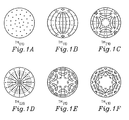
- Figs. 1A-1F disclose, for illustrative purposes, the lower order TM nmp field distributions for a circular parallel plate resonator, i.e. the TM 010 , TM 110 , TM 210 , TM 020 , TM 310 , TM 410 -modes.
- Solid lines indicate the current
- dashed lines indicate the magnetic field
- the field/current distributions are fixed in space by coupling arrangements (such as coupling loops, coupling probes, or a further resonator).
- Parallel plate resonators for example in the form of circular dielectric disks and circular patches on dielectric substrates, have found several different microwave applications.
- the resonators are seen as electrically thin if the thickness (d) is smaller than half the wavelength of the microwave ( ⁇ g ) in the resonator, d ⁇ g /2, so that no standing waves will be present along the axis of the disk.
- Electrically tunable resonators based on circular ferroelectric disks have been largely investigated for applications in tunable filters.
- the third index is 0.
- the above formula may be corrected taking fringing fields into account.
- the mode selected for the resonators is the TM 020 mode.
- the invention is however not limited to any particular mode but substantially any mode could be selected. Mode selection is among others discussed in "Microwave Device and Method Relating Thereto" with Application No. 9901190-0 as discussed earlier in the application.
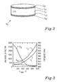
- Fig. 2 schematically illustrates an electronically tunable resonator 10 0 based on a non-linear dielectric substrate 3 0 with an extremely high dielectric constant, e.g. STO (SrTiO 3 which has a dielectric constant of more than 2000 at the temperature of liquid nitrogen (N) and a dielectric constant of about 300 at room temperature.
- an extremely high dielectric constant e.g. STO (SrTiO 3 which has a dielectric constant of more than 2000 at the temperature of liquid nitrogen (N) and a dielectric constant of about 300 at room temperature.
- STO STO
- N liquid nitrogen
- the resonant frequencies of a circular parallel plate disk resonator having a diameter of 10 mm and a thickness of 0.5 mm will be in the range of 0.2-2.0 GHz depending on the temperature and on the applied DC biasing.
- Such resonators can be excited by simple probes or loops as in/out coupling means.
- the thickness of a parallel plate resonator is much smaller than the wavelength of the microwave signal in order for the resonator to support only the lowest order TM-modes, and in order to keep the DC-voltages, which are required for the electrical tuning of the resonator with a non-linear dielectric substrate as low as possible.
- Fig. 3 schematically illustrates a diagram indicating the measured microwave performance of two resonators.
- the unloaded quality factor, Q as a function of the biasing voltage, is illustrated for a resonator in which normally conducting, i.e. non-superconducting, electrode plates are used, corresponding to Q II , and for a resonator in which HTS electrodes of YBCO are used, corresponding to lines Q I .
- the resonant frequencies are illustrated as a function of the applied biasing voltage, corresponding to F I , F II for Cu electrodes and for YBCO electrodes respectively. It can be seen that at high biasing voltages, it does not make much difference whether YBCO electrodes are used or if normally conducting (non-superconducting) electrode are used.
- the resonant frequency of a such resonator should be between 0.5-3GHz, which is the frequency region of cellular communication systems.
- a resonator apparatus comprising two coupled resonators, e.g. as described in Fig. 4 , to provide for a so called loss compensation.
- a first embodiment of the present invention is illustrated. It shows a resonator arrangement 10 comprising a resonator apparatus with a first resonator 1 and a second resonator 2, which resonators are coupled to each other.
- the first resonator comprises a circular disk resonator with a first electrode plate 12, and a linear substrate 11 with a high quality factor (Q) which is not tunable.
- the substrate material may for example comprise sapphire, LaAlO 3 or any of the other materials referred to earlier in the application.
- the first resonator 1 comprises another electrode plate 13 disposed on the other side of the linear substrate.
- the electrodes 12, 13 may comprise a "normally" conducting (i.e.
- non-superconducting, but preferably high conductivity metal such as for example Au, Ag, Cu but they may also comprise a superconducting material.
- the electrode plates 12, 13 comprise a high temperature superconducting material, e.g. YBCO.
- the resonator apparatus 10 further comprises a second resonator 2, which is tunable and comprises a substrate material 21 of e.g. a ferroelectric material, e.g. SrTiO 3 , KTaO 3 or any other of the materials as referred to earlier in the application having a growing loss factor, i.e. for which the quality factor decreases with the applied voltage as discussed above with reference to Fig. 3 .
- the second resonator 2 is a circular disk resonator with a first electrode plate 22 and a second electrode plate 13, which is the same electrode plate as the second electrode of the first resonator 1.
- the common electrode 13 forms a common ground plane for the first and second resonators 1,2.
- the first and second resonators 1,2 are coupled to each other through coupling means 5, here comprising a slot or an aperture in the common ground plane 13 allowing for distributing of electromagnetic energy between the two resonators upon application of a biasing voltage.
- biasing means 3 are provided comprising a variable voltage source which is connected to the ground plane 13 and to the first electrode 22 of the second resonator 2, such that for tuning of the resonator apparatus, the biasing voltage is applied to the second resonator 2.
- V B biasing voltage
- the biasing voltage V B When the biasing voltage V B is applied and increased, the resonant frequency of the second resonator 2 will increase.
- Electromagnetic energy will then be relocated to the first resonator 1, which means that the increased loss tangent of the second resonator, which, as discussed above, increases as the biasing voltage is increased, will have a low influence on the resonator apparatus as such. Thus, as the biasing voltage increases, more and more electromagnetic energy will be transferred or redistributed to the first resonator 1. In this manner the increased loss in the tunable second resonator 2 will be compensated for.
- the coupling slot is circular; which shape it should have depends on the mode(s) that is/are selected.
- the current lines cf. Figs 1A-1F ) should not be interrupted. Normally it functions with a circular slot for all modes. It may also be ellipsoidal. For a rectangular resonator it may be rectangular.
- the first and second resonators may also have other shapes, the same or different.
- the ground plane may also have the same size (and shape) as the first resonator or any other shape as long as it is not smaller than the first resonator.
- input coupling means 4 in the form of an antenna are shown for input of microwave signals to the microwave device for exciting the relevant mode or modes.
- any input/output coupling means can be used and the antenna is merely indicated for indication of an example on input coupling means.
- Different types of input/output coupling means are discussed in the Swedish patent application “Arrangement and Method Relating to Microwave Devices” filed on April 18, 1997 with the application No. 9701450-0 .
- the coupling means can be used for application of a biasing voltage. It also illustrates examples on coupling means that can be used while still requiring separate biasing means, as well as a number of state of the art devices.
- the present invention is not limited to any particular way of coupling microwave energy into/out of the device, the main thing being that the biasing voltage is applied to the second resonator, which is tunable, and which is coupled to another resonator which is not tunable, which resonators are coupled to one another such that redistribution of electromagnetic energy is enabled.
- the second resonator 2 may also be a thin parallel plate microwave resonator, thin here meaning that it is thin in comparison with the wavelength in the resonator, ⁇ g , more specifically d ⁇ g /2, wherein d is the thickness of the resonator 2, and ⁇ g is the wavelength in the resonator.
- ⁇ g the wavelength in the resonator.
- the apparatus could be a thin film device, although bulk substrate devices are preferred, as discussed earlier.
- Fig. 5 the equivalent circuit of the two coupled resonators 1,2 of Fig. 4 is illustrated.
- Z in represents the input impedance of the arrangement
- R 1 , C 1 represent the resistor and the capacitor of the first, non-tunable resonator 1.
- R 2 , C 2 represent the tunable components of the second resonator 2, and
- C 0 5 is the coupling capacitor coupling the first and second resonators to each other.
- Figs. 6A,6B , 7A,7B,7C follows an illustration and explanation of a simulation of the input impedance of the equivalent circuit of Fig. 5 .
- d 1 is the loss factor of the linear dielectric substrate of the first resonator
- d 2 (U) is the loss factor of the non-linear ferroelectric substrate of the second resonator as a function of the biasing voltage.
- the biasing voltage V is given in Volts, L (the inductance) in nH.
- U 0 and k are phenomenological characteristics of the ferroelectric material.
- C1 2.5 pF
- C20 120 pF
- C 0 200 pF
- L 1.59 x 10 -9
- m 0.115
- L2 0,0517 x 10 -9 H
- LO L x m
- L00 L x (1-m).
- C ⁇ 2 U C ⁇ 20 / 1 + U / U ⁇ 0 2
- d ⁇ 2 U d ⁇ 20 ⁇ 1 + k ⁇ ⁇ U / U ⁇ 0 2 .
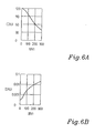
- Fig. 6A illustrates the dependence of C2(U) on the applied voltage U
- Fig. 6B illustrates the dependence of d2(U) on the applied biasing voltage.
- the input impedance of the second resonator is given by:
- Z ⁇ 2 f U i ⁇ ⁇ f ⁇ L ⁇ 2 + 10 12 i ⁇ ⁇ f ⁇ C ⁇ 2 U ⁇ 1 + i ⁇ d ⁇ 2 U
- Figs. 7A illustrate the real and imaginary parts of the input impedance at zero applied voltage.
- Figs. 7B, 7C illustrates the real and imaginary parts of the impedance at a biasing voltage of 100V and 200V respectively.
- the resonant frequency will be about 2459.4 MHz
- a biasing voltage of 100V it will be 2509.3 MHz
- for an applied biasing voltage of 200V it will be about 2530.9 MHz.
- the frequency shift ⁇ F will be 49.9 MHz for 100V and 71.5 MHz for 200 V biasing voltage.
- the loss factor of the ferroelectric, tunable substrate material will change about 30 times.
- the total quality factor change will be no more than about ⁇ 30%. If the frequency band of the resonator is about 0.5 MHz, the resonator figure of merit will be ⁇ F/ ⁇ f ⁇ 71.5/0.5 ⁇ 140. It should however be clear that Figs. 6A,6B , 7A,7B,7C merely are included for illustrative and exemplifying purposes.
- Fig. 8A shows one particular example of a first resonator 1A e.g. as in Fig. 4 , which comprises a circular disk resonator. It comprises a non-tunable, high quality linear substrate 11A, a first conducting electrode 12A, which for example may be superconducting or even high temperature superconducting, and a second electrode 13A which for example is a larger than the substrate 11A and the first electrode 12A. It may for example also have the same size as the first electrode 12A.
- This second electrode plate 13A acts as a common ground plane for the first resonator 1A and for the second resonator 2A of Fig. 8B .
- the common ground plane 13 comprises coupling means 5A for coupling the first resonator 1A and the second resonator 2A to each other.
- the second resonator 2A comprises a first electrode 22A disposed on a ferroelectric substrate e.g. of STO which is non-linear and has an (extremely) high dielectric constant.
- Biasing means comprising a variable voltage source V o 3 with connection leads is connected to the common ground plane 13A and to the first electrode plate 22A of the second resonator 2A.
- the TM 020 modes are excited via input coupling means (not shown in this figure).
- the coupling means 5A may comprise a slot which is circular or ellipsoidal, and through which electromagnetic energy from the second resonator 2A can be redistributed to the first resonator 1A upon application of a biasing voltage to the second resonator 2A.
- Figs. 9A, 9B in a manner similar to that of Figs. 8A, 8B illustrate a first resonator 1B ( Fig. 9A ) and a second resonator 2B ( Fig. 9B ) together forming an alternative resonator apparatus in which the first and second resonators 1B, 2B are square-shaped.
- the first resonator 1B like in the preceding embodiment, comprises a linear material with a high quality which is non-tunable, e.g. of LaAlO 3
- the second resonator 2B comprises a tunable ferroelectric material e.g. of STO.
- the first resonator 1B comprises a first electrode plate 12B which of course can be similar to the electrode plate of Fig. 8A with the difference that it is square-shaped, but it may also, as illustrated in the figure, comprise a very thin, (thin in order not to affect the surface impedance) superconducting layer 12B 1 covered, on the side opposite to the substrate, by a non-superconducting high conductivity film 12B 2 e.g. of Au, Ag, Cu or similar for protective purposes.
- the superconducting film is high temperature superconducting, e.g. of YBCO.
- the second resonator 2B comprises a first electrode plate 22B with a (high temperature) superconducting layer 22B 1 covered by a non-superconducting metal layer 22B 2 .
- the first and second resonator 1B, 2B like in the preceding embodiment, comprise a common ground plane, for both forming a second electrode 13B which, in this particular implementation, comprises a (high temperature) superconducting layer 13B 1 covered on either side by a very thin non-superconducting metal film 13B 2 , 13B 3 .
- the ground plane just consists of a superconducting layer.
- a biasing voltage is applied between the first and second electrodes 22B, 13B of the second resonator 2B and electromagnetic energy can be redistributed via coupling means 5B, which here comprises a rectangular slot, to the first resonator 1B.
- coupling means 5B which here comprises a rectangular slot
- the coupling means does not have to be a rectangular slot, but it can be any kind of aperture giving the desired properties as far as transfer of electromagnetic energy is concerned for the concerned modes. It may e.g. be circular or ellipsoidal as well. Still further the electrodes may consist of normal metal only.
- the inventive concept is also applicable to dual mode operating resonators, oscillators, filters whereby dual mode operation can be provided for in different manners, e.g. as disclosed in the patent application "Tunable Microwave Devices" referred to above.
- Fig. 10 for illustrative purposes shows a very simplified top view of a dual mode resonator apparatus comprising input 4C in and output 4C out coupling means and a protruding portion 6 for providing coupling enabling dual mode operation.
- a dual mode operating resonator apparatus can also be provided for by rectangularly shaped resonators or in any other appropriate manner.
- the coupling slot for coupling between the first and second resonator is illustrated by the dashed line circle.
- the inventive concept is extended to a tunable filter 100, cf. Fig. 11 .
- two resonator apparatuses 10D, 10E are provided each comprising a first resonator 1D, 1E respectively and a second resonator 2D, 2E respectively, which share a common ground plane 13F.
- the first resonators 1D,1E comprise a common substrate 11C. There may alternatively be separate substrates.
- the distance between the resonator apparatuses gives the coupling strength of the filter.
- the resonator apparatuses comprise circular disk resonators as described in for example Figs.
- Fig. 12 illustrates the equivalent circuit of a two-pole filter 100 as in Fig. 11 which is connected by a transmission line section.
- the first resonator apparatus 10D with resistance R 1D and capacitance C 1D corresponding to the first non-tunable resonator 1D and the tunable resonator 2D comprising a resistor R 2D and capacitor C 2D which resonators are coupled to each other by the coupling means 5D represented by a capacitor C 04 .
- the inductances L 04 , L 004 ; L 05 , L 005 of the resonators are also illustrated in the figure as explained earlier with reference to Fig. 6A, 6B , 7A, 7B .
- a second resonator apparatus 10E comprising a first resonator 1E and second resonator 2E with the respective non-tunable and tunable components resistance R 1E , C 1E and R 2E , C 2E respectively and connecting capacitor C 05 corresponding to coupling means 5E.
- the two-pole filter is connected by a transmission line section.
- the characteristic impedance of the external line Z 0 50 Ohm
- the characteristic impedance of the coupling line Z 01 45 Ohm
- the electrical length of the coupling line at the central frequency is 80°.
- Figs. 13A, 13B are diagrams showing simulated lines of the tunable two-pole filter of Fig. 10 .
- the insertion losses in dB and the return losses in dB correspond to the transmissions T and the reflectivity.
- ⁇ is given for three different values of a biasing voltage V.
- T1 corresponds to the transmission as a function of the frequency at zero biasing voltage
- T 2 corresponds to the transmission as a function of the frequency in GHz for a biasing voltage of 100V
- T 3 is the transmission for a biasing voltage of 200V.
- the reflectivities ⁇ 1 , ⁇ 2 , ⁇ 3 are indicated in Fig. 13B for biasing voltages 0V, 100V, 200V.
- the insertion losses and the return losses are maintained even at a higher biasing voltage.
- the average bandwidth is 15 MHz, and the range of tunability is approximately 70 MHz with an insertion loss ⁇ 0.5 dB.
- the drastically increasing loss factor of the ferroelectric material of the second resonator is largely compensated for through the application of the inventive concept.
- the resonators may be of other different shapes, they may comprise different substrate materials as discussed in the foregoing, they may comprise non-superconducting or particularly (high temperature) superconducting electrodes etc. They may also be single mode operating or dual mode operating and any appropriate type of coupling means may be provided for coupling in of electromagnetic energy to excite the desired modes, i.e. the modes which are selected, particularly the TM 020 modes. However, also other modes can be selected in any appropriate manner.
Abstract
Description
- The present invention relates to a tunable resonating arrangement which comprises a resonator apparatus. Electromagnetic energy is coupled into/out of the resonator apparatus over input/output coupling means, and for tuning of the resonator apparatus, a tuning device is used for application of a biasing/tuning voltage (electric field) to the resonator apparatus. The resonator apparatus comprises a first non-tunable resonator and a second resonator, which is tunable and comprises a ferroelectric substrate. Coupling means are provided for coupling between the first and second resonators, which are separated by a ground plane common for the first and second resonators. The invention also relates to a method of tuning a resonating arrangement.
- Electrically tunable resonators are attractive components for agile radar and mobile radio communication systems. Different types of resonators are known. Dielectric and parallel plate resonator and filters for microwave frequencies using dielectric disks of any shape, for example circular, are known e.g. from Vendik et al., Electronics Letters vol. 31, p. 654, 1995.
- Parallel plate resonators comprising substrates of non-linear dielectric materials with extremely high dielectric constants, for example ferroelectric materials or anti-ferroelectric materials, have small dimensions, and they can for example be used to provide very compact filters in the frequency bands in which advanced microwave communication systems operate. Such non-linear dielectric materials may e.g. be STO(SrTiO3) with a dielectric constant of about 2000 at the temperature of liquid nitrogen and a dielectric constant of about 300 at room temperature.
- Dielectric, parallel plate resonators can be excited by simple probes or loops. For the majority of practical implementations the thickness of a parallel plate resonator is much smaller than the wavelength of the microwave signal in the resonator in order for the resonator to support only the lowest order TM modes and in order to keep the DC-voltages, which are required for the electrical tuning of the resonator comprising a dielectric substrate with electrodes arranged on both sides of it, as low as possible. For such resonators electrical tuning is obtained by means of the application of an external DC-biasing voltage, which is supplied by means of ohmic contacts to the electrodes acting as plates of the resonator. Tunable resonators based on thin film substrates as well as resonators based on dielectric bulk substrates are known. A resonator is considered to be electrically thin if the thickness is smaller than half the wavelength of the microwave signal in the resonator such that no standing waves will be present along the axis of the disk. Electrically tunable resonators based on circular ferroelectric disks have recently been found attractive and have drawn much attention for example for applications as tunable filters in microwave communication systems, as well as in mobile radio communication systems.
- Such devices are for example described in "Tunable Microwave Devices", which is a Swedish patent application with application number 9502137-4 and "Arrangement and method relating to tunable devices" which is a Swedish patent application with application number
9502138-2 - Substrates comprising ferroelectric materials in resonators and filters are of interest for different reasons. Among other things ferroelectric materials are able to handle high peak power, they have a low switching time, and the dielectric constant of the substrate varies with an applied biasing voltage, which makes the impedance of the device vary with an applied biasing electric field. For example
US-A-5 908 811 , "High Tc Superconducting Ferroelectric Tunable Filters", shows an example of such a filter which should get low losses by means of using a single crystal ferroelectric material. A ferroelectric thin film substrate is used. However, this device as well as other resonators and filters based on ferroelectric materials suffer from the drawback of the quality factor (Q-value) of the ferroelectric substrate or element decreasing drastically with the applied voltage, when a biasing voltage is applied. This has recently been established by A. Tagantsev in "DC-Electric-Field-induced microwave loss in ferroelectrics and intrinsic limitation for the quality factor of a tunable component", Applied Physics Letters, Vol. 76, No. 9, p. 1182-84, to be a consequence of a fundamental loss mechanism (called quasi-Debye Effect) induced in the ferroelectric material by the applied biasing field. -
US-A-5 935 910 shows an example of a high power band-pass filter which is made of two waveguide cavities (resonators) limited by respective irises. Both cavities are tunable and comprise hollow waveguides loaded by ferroelectric rings. Electrodes of the rings are formed on the inside and outside of cylindrical surfaces and the rings are used to perturb or tune the hollow cavities (resonators) between the irises. - However, so far, no satisfactory solution to the problem associated with induced losses in tunable ferroelectric resonators has been found.
- What is needed is therefore a tunable resonating arrangement, more particularly for microwaves or millimeter waves, which has small dimensions and which can be used in different kinds of advanced microwave communication systems and mobile radio communication systems. A tunable resonator arrangement is also needed which has a high, or at least satisfactory, performance, and which is easy to fabricate. Particularly a tunable resonating arrangement is needed through which it is possible to compensate for the losses in a ferroelectric substrate upon application of an electric field/voltage for tuning purposes. Particularly an arrangement is needed which has a high power handling capability. Even more particularly an arrangement is needed through which tuning by the means of the application of a DC-biasing can be provided substantially without deteriorating. the quality factor (Q-value) of the resonator.
- An arrangement is also needed which is compact in size for use in different types of components, which can be tuned efficiently without requiring too high amounts of power, and which is reliable in operation. Moreover an arrangement is needed which is robust and which has a satisfactory tuning selectivity and tuning sensitivity, and through which the insertion losses are low or can be compensated for.
- A tunable filter arrangement is also needed which comprises one a more resonator apparatuses and which meets one or more of the objects referred to above. Still further a method of tuning a resonator arrangement is needed through which the above mentioned objects can be achieved, and particularly a method of compensating for the losses induced in a ferroelectric resonator substrate through electrical or electronical tuning.
- Therefore a tunable resonating arrangement as initially referred to is provided wherein the first resonator is a parallel plate resonator which comprises a dielectric bulk or thin film disk substrate with a first electrode plate disposed on one side of the dielectric substrate and a second electrode plate disposed on the other side of the dielectric substrate, the electric permittivity of which substantially does not vary with applied biasing voltage. The second resonator comprises a tunable ferroelectric substrate bulk or thin film disk substrate with a first electrode plate disposed on one side of the ferroelectric substrate and a second electrode plate disposed on the other side of the ferroelectric substrate. The second electrode plate of the second resonator is the same as the second electrode plate of the first resonator and forms the said common ground plane. For tuning of the resonator apparatus, the biasing voltage/electric field is applied to the second resonator.
- The dielectric substrate of the first resonator may for example comprised LaAlO3, MgO, NdGaO3 Al2O3, sapphire or a material with similar properties. Particularly the quality factor (Q-value) of the first resonator may exceed approximately 105-5·105.
- The substrate of the second resonator may for example comprise SrTiO3, KTaO3, or BaSTO3 or any other material with similar properties.
- The first and second electrodes of each resonator, which here means the first electrodes and the common ground plane, in one implementation consist of normal conducting metal, such as for example Au, Ag, Cu. In another implementation the first and second electrodes, i.e. the first electrodes and the common ground plane, consist of a superconducting material. Even more particularly the first and second electrodes, i.e. the first electrodes and the common ground plane, consist of a high temperature superconducting material (HTS), for example YBCO (Y-Ba-Cu-O). Other alternatives are TBCCO and BSCCO. In a particular implementation superconductors or superconducting films (HTS) are used, which may be covered by thin non-superconducting high conductivity films of for example Au, Ag, Cu or similar. Such devices are also discussed in "Tunable Microwave Devices" referred to above. Particularly the first and second resonators are TM020 mode resonators. However, also other modes can be selected, as discussed example in the Swedish patent application "Microwave Devices and Method Relating Thereto" with application number
9901190-0 - Through the application of a tuning (biasing) voltage to said second resonator, electromagnetic energy will be distributed to the first resonator and, particularly, as the biasing voltage increases, more and more electromagnetic energy will be distributed or transferred to the first resonator since the resonators are coupled the way they are. This means that the distribution of electromagnetic energy between the first and second resonators depends on the biasing (tuning) voltage or the electric field and of course the coupling means. The resonating frequency in the second resonator increases with the application of an increasing biasing voltage. As the biasing voltage increases, also the loss tangent of the second, ferroelectric, resonator will increase, at the same time as less of the electromagnetic energy will be located in it. Thereby will automatically be compensated for the increased loss tangent of the second resonator in that the influence thereof on the coupled resonator apparatus comprising the first and the second resonators will be reduced.
- Particularly the first and second resonators comprise disk resonators based on a dielectric/ferroelectric bulk material. They may however also comprise thin film substrates. However, by using tunable disk resonators resonating arrangements, particularly filters, which have a much higher power handling capability than those made of tunable thin film, can be realized.
- Particularly the resonating arrangement comprises at least two resonator apparatuses, and the common ground plane is common for (shared by) the at least two resonator apparatuses to form a tunable filter.
- According to the invention, for coupling a first and a second resonator to each other, the coupling means may comprise, for each resonator apparatus, a slot or an aperture in the common ground plane. The resonators may be of substantially any appropriate shape, they may e.g. be circular, square-shaped, rectangular or ellipsoidal etc. The shape of the first resonator may also differ from that of the second resonator. The resonator apparatus may also be a dual mode resonator apparatus. Then each resonator comprises mode coupling means such as for example a protrusion, a cut-out or any other means to provide for dual mode operation. According to the invention it can be said that tunability and losses is exchanged or distributed between the two resonators of a resonator apparatus, thereby reducing the effect of the induced increasing losses caused by the electrical tuning.
- According to the invention thus a tunable resonator apparatus is provided which comprises a first resonator and a second resonator, wherein in said first resonator is non tunable, said second resonator is tunable and ferroelectric, i.e. comprises a ferroelectric substrate, whereby said first and second resonators are separated by a ground plane which is common for said first and second resonators. Coupling means are provided for providing coupling between said first and second resonators, and for tuning of the resonator apparatus, a tuning voltage is applied to the second resonator. Particularly the first and the second resonator comprises disk resonators or parallel plate resonators, and the common ground plane is formed by a second electrode plate of the first resonator which is common with a second electrode plate of the second resonator. The coupling means particularly comprises a slot or an aperture or similar in the common ground plane, through which electromagnetic energy can be transferred from one of the resonators to the other.
- The invention also discloses a method of tuning a resonator apparatus which comprises the steps of; providing a first, non-tunable resonator; providing a second tunable resonator; providing coupling means such that the first and second resonators become coupled, allowing transfer of electromagnetic energy between the first and second resonators; applying a biasing, tuning, voltage to said second resonator. The method is characterized in that the first resonator is a parallel plate resonator with a disk bulk or thin film dielectric substrate and with a first electrode plate disposed on one side of the dielectric substrate and a second electrode plate disposed on the other side of the dielectric substrate, the electric permittivity of which substantially does not vary with applied biasing voltage.
- The second resonator comprises a tunable ferroelectric substrate bulk or thin film disk substrate with a first electrode plate disposed on one side of the ferroelectric substrate and a second electrode plate disposed on the other side of the ferroelectric substrate.
- The second electrode of the second resonator is the same as the second electrode plate of the first resonator and forms a common ground plane, and further comprises: applying the biasing, tuning, voltage to the second resonator while optimizing the application of the biasing voltage such that the influence of the increased loss tangent in the first resonator, or the coupled resonator apparatus, will be compensated for, by an increased transfer of electromagnetic energy to the first resonator via the coupling means.
- The invention will in the following be further described in a non-limiting manner and with reference to the accompanying drawings, in which:
- Figs. 1A-1F
- for illustrative purposes show the current lines (field distributions) for a number of different TM modes of a circular, parallel plate resonator,
- Fig. 2
- particularly illustrates a state of the art resonator having a field distribution as in
Fig. 1A , - Fig. 3
- shows the measured microwave performance of the resonator in
Fig. 2 , - Fig. 4
- illustrates a cross-sectional view of a first embodiment of a resonator apparatus according the present invention,
- Fig. 5
- illustrates the equivalent circuit of the two coupled resonators of the resonator apparatus in
Fig. 4 , - Fig. 6A
- is a diagram illustrating a dependence of the capacitance of the resonator as a function of the biasing voltage,
- Fig. 6B
- diagram illustrating the loss factor as function of biasing voltage,
- Figs. 7A-7C show
- simulated results of the dependence of the input impedances, of the equivalent circuit, on biasing voltage,
- Fig. 8A
- schematically illustrates one example of a first resonator that can be used in the resonator apparatus of
Fig. 4 , - Fig. 8B
- schematically illustrates an example of a resonator that can be used as a second resonator in the resonator apparatus of
Fig. 4 , - Fig. 9A
- shows an alternative implementation of a first resonator of a resonator apparatus according to the invention,
- Fig. 9B
- illustrates an example of a second resonator that can be used with the first resonator of
Fig. 9A in a resonator apparatus according to the invention, - Fig. 10
- very schematically illustrates an example of a dual mode resonator that can be used in a resonator apparatus according to the invention,
- Fig. 11
- schematically illustrates a two-pole filter based on a resonating arrangement according to the present invention,
- Fig. 12
- illustrates the equivalent circuit for the two-pole filter of
Fig. 11 , - Figs. 13A,B
- illustrate simulated results of the insertion losses and the return losses as functions of the frequency for different values of the biasing voltage for a tunable two-pole filter as in
Fig. 11 . -
Figs. 1A-1F disclose, for illustrative purposes, the lower order TMnmp field distributions for a circular parallel plate resonator, i.e. the TM010, TM110, TM210, TM020, TM310, TM410-modes. Solid lines indicate the current, dashed lines indicate the magnetic field and dots and crosses indicate the electric field. It is supposed that p=0, i.e. that the thickness of the substrate is smaller than half a wavelength in the resonator, and that the resonator only supports TMnm0-modes. The field/current distributions are fixed in space by coupling arrangements (such as coupling loops, coupling probes, or a further resonator). - Parallel plate resonators, for example in the form of circular dielectric disks and circular patches on dielectric substrates, have found several different microwave applications. The resonators are seen as electrically thin if the thickness (d) is smaller than half the wavelength of the microwave (λg) in the resonator, d<λg/2, so that no standing waves will be present along the axis of the disk. Electrically tunable resonators based on circular ferroelectric disks have been largely investigated for applications in tunable filters. A simplified electrodynamic analysis of a parallel plate resonator proposes a simple formula for the resonant frequency:

where c0=3.108m/s is the velocity of light in vacuum, ε is the relative dielectric constant of the disk/substrate, r is the radius of the conducting plate, and knm are the roots of Bessel functions with mode indexes n and m. For an electrically thin parallel-plate resonator the third index is 0. The above formula may be corrected taking fringing fields into account. - Particularly attractive for filter applications are for example the axially symmetric modes with plate currents only in the radial direction. These modes are characterized by higher quality factors (Q) since they do not have any surface currents along the edges of the conductor plates.
- In a particularly advantageous implementation of the present invention, the mode selected for the resonators is the TM020 mode. The invention is however not limited to any particular mode but substantially any mode could be selected. Mode selection is among others discussed in "Microwave Device and Method Relating Thereto" with Application No.
9901190-0 -
Fig. 2 schematically illustrates an electronicallytunable resonator 100 based on a non-lineardielectric substrate 30 with an extremely high dielectric constant, e.g. STO (SrTiO3 which has a dielectric constant of more than 2000 at the temperature of liquid nitrogen (N) and a dielectric constant of about 300 at room temperature. On both sides of the substratehigh temperature superconductors high conductivity films Fig. 1A above, for the TM010 mode, and inFig. 1D for the TM020 mode. -
Fig. 3 schematically illustrates a diagram indicating the measured microwave performance of two resonators. In the figure the unloaded quality factor, Q, as a function of the biasing voltage, is illustrated for a resonator in which normally conducting, i.e. non-superconducting, electrode plates are used, corresponding to QII, and for a resonator in which HTS electrodes of YBCO are used, corresponding to lines QI. Correspondingly the resonant frequencies are illustrated as a function of the applied biasing voltage, corresponding to FI, FII for Cu electrodes and for YBCO electrodes respectively. It can be seen that at high biasing voltages, it does not make much difference whether YBCO electrodes are used or if normally conducting (non-superconducting) electrode are used. - Advantageously the resonant frequency of a such resonator should be between 0.5-3GHz, which is the frequency region of cellular communication systems. Thus, the problem of the Q - values of the ferroelectric elements, or non-linear dielectric materials, as discussed above, decreasing drastically with the applied electric field, according to the invention is solved by means of a resonator apparatus comprising two coupled resonators, e.g. as described in
Fig. 4 , to provide for a so called loss compensation. - Thus, in
Fig. 4 a first embodiment of the present invention is illustrated. It shows aresonator arrangement 10 comprising a resonator apparatus with afirst resonator 1 and asecond resonator 2, which resonators are coupled to each other. The first resonator comprises a circular disk resonator with afirst electrode plate 12, and alinear substrate 11 with a high quality factor (Q) which is not tunable. The substrate material may for example comprise sapphire, LaAlO3 or any of the other materials referred to earlier in the application. Thefirst resonator 1 comprises anotherelectrode plate 13 disposed on the other side of the linear substrate. Theelectrodes electrode plates - The
resonator apparatus 10 further comprises asecond resonator 2, which is tunable and comprises asubstrate material 21 of e.g. a ferroelectric material, e.g. SrTiO3, KTaO3 or any other of the materials as referred to earlier in the application having a growing loss factor, i.e. for which the quality factor decreases with the applied voltage as discussed above with reference toFig. 3 . Also thesecond resonator 2 is a circular disk resonator with afirst electrode plate 22 and asecond electrode plate 13, which is the same electrode plate as the second electrode of thefirst resonator 1. - Thus the
common electrode 13 forms a common ground plane for the first andsecond resonators second resonators common ground plane 13 allowing for distributing of electromagnetic energy between the two resonators upon application of a biasing voltage. For application of said biasing voltage, biasing means 3 are provided comprising a variable voltage source which is connected to theground plane 13 and to thefirst electrode 22 of thesecond resonator 2, such that for tuning of the resonator apparatus, the biasing voltage is applied to thesecond resonator 2. When the biasing voltage VB is applied and increased, the resonant frequency of thesecond resonator 2 will increase. Electromagnetic energy will then be relocated to thefirst resonator 1, which means that the increased loss tangent of the second resonator, which, as discussed above, increases as the biasing voltage is increased, will have a low influence on the resonator apparatus as such. Thus, as the biasing voltage increases, more and more electromagnetic energy will be transferred or redistributed to thefirst resonator 1. In this manner the increased loss in the tunablesecond resonator 2 will be compensated for. - Preferably the coupling slot is circular; which shape it should have depends on the mode(s) that is/are selected. Generally the current lines (cf.
Figs 1A-1F ) should not be interrupted. Normally it functions with a circular slot for all modes. It may also be ellipsoidal. For a rectangular resonator it may be rectangular. - The first and second resonators may also have other shapes, the same or different. The ground plane may also have the same size (and shape) as the first resonator or any other shape as long as it is not smaller than the first resonator.
- In the figure input coupling means 4 in the form of an antenna are shown for input of microwave signals to the microwave device for exciting the relevant mode or modes. In principle any input/output coupling means can be used and the antenna is merely indicated for indication of an example on input coupling means. Different types of input/output coupling means are discussed in the Swedish patent application "Arrangement and Method Relating to Microwave Devices" filed on April 18, 1997 with the application No.
9701450-0 - One example of a second resonator that can be used in a resonator apparatus according to the present invention was disclosed in
Fig. 3 . Thesecond resonator 2 may also be a thin parallel plate microwave resonator, thin here meaning that it is thin in comparison with the wavelength in the resonator, λg, more specifically d<λg/2, wherein d is the thickness of theresonator 2, and λg is the wavelength in the resonator. (Generally the apparatus could be a thin film device, although bulk substrate devices are preferred, as discussed earlier.) - In
Fig. 5 the equivalent circuit of the two coupledresonators Fig. 4 is illustrated. Zin represents the input impedance of the arrangement R1, C1 represent the resistor and the capacitor of the first,non-tunable resonator 1. R2, C2 represent the tunable components of thesecond resonator 2, andC 0 5 is the coupling capacitor coupling the first and second resonators to each other. - With reference to
Figs. 6A,6B ,7A,7B,7C follows an illustration and explanation of a simulation of the input impedance of the equivalent circuit ofFig. 5 . It is here supposed that d1 is the loss factor of the linear dielectric substrate of the first resonator and d2(U) is the loss factor of the non-linear ferroelectric substrate of the second resonator as a function of the biasing voltage. The biasing voltage V is given in Volts, L (the inductance) in nH. U0 and k are phenomenological characteristics of the ferroelectric material. The simulations are done for three different biasing voltages, namely for V = 0, 100, 200V and U0 = 200V. It is further supposed that C1 = 2.5 pF, C20 = 120 pF, and C0 = 200 pF. L = 1.59 x 10⁻⁹, m = 0.115, L2 = 0,0517 x 10⁻⁹ H, d20 = 3 x 10⁻⁴ and k = 30, LO = L x m and L00 = L x (1-m).
-
Fig. 6A illustrates the dependence of C2(U) on the applied voltage U andFig. 6B illustrates the dependence of d2(U) on the applied biasing voltage. The input impedance of the first resonator is given by:
and the input impedance of the second resonator is given by:
- Thus the input impedance of the equivalent circuit will be:

-
Figs. 7A illustrate the real and imaginary parts of the input impedance at zero applied voltage. CorrespondinglyFigs. 7B, 7C illustrates the real and imaginary parts of the impedance at a biasing voltage of 100V and 200V respectively. As can be seen from the figures, for zero biasing voltage the resonant frequency will be about 2459.4 MHz, for a biasing voltage of 100V it will be 2509.3 MHz and for an applied biasing voltage of 200V it will be about 2530.9 MHz. The frequency shift ΔF will be 49.9 MHz for 100V and 71.5 MHz for 200 V biasing voltage. In the given range of the applied voltage, the loss factor of the ferroelectric, tunable substrate material will change about 30 times. However, the total quality factor change will be no more than about ±30%. If the frequency band of the resonator is about 0.5 MHz, the resonator figure of merit will be ΔF/Δf ≈ 71.5/0.5 ≈ 140. It should however be clear thatFigs. 6A,6B ,7A,7B,7C merely are included for illustrative and exemplifying purposes. -
Fig. 8A shows one particular example of afirst resonator 1A e.g. as inFig. 4 , which comprises a circular disk resonator. It comprises a non-tunable, high qualitylinear substrate 11A, afirst conducting electrode 12A, which for example may be superconducting or even high temperature superconducting, and asecond electrode 13A which for example is a larger than thesubstrate 11A and thefirst electrode 12A. It may for example also have the same size as thefirst electrode 12A. Thissecond electrode plate 13A acts as a common ground plane for thefirst resonator 1A and for thesecond resonator 2A ofFig. 8B . Thecommon ground plane 13 comprises coupling means 5A for coupling thefirst resonator 1A and thesecond resonator 2A to each other. - The
second resonator 2A comprises afirst electrode 22A disposed on a ferroelectric substrate e.g. of STO which is non-linear and has an (extremely) high dielectric constant. Biasing means comprising a variablevoltage source V o 3 with connection leads is connected to thecommon ground plane 13A and to thefirst electrode plate 22A of thesecond resonator 2A. Preferably the TM020 modes are excited via input coupling means (not shown in this figure). The coupling means 5A may comprise a slot which is circular or ellipsoidal, and through which electromagnetic energy from thesecond resonator 2A can be redistributed to thefirst resonator 1A upon application of a biasing voltage to thesecond resonator 2A. -
Figs. 9A, 9B in a manner similar to that ofFigs. 8A, 8B illustrate afirst resonator 1B (Fig. 9A ) and asecond resonator 2B (Fig. 9B ) together forming an alternative resonator apparatus in which the first andsecond resonators first resonator 1B, like in the preceding embodiment, comprises a linear material with a high quality which is non-tunable, e.g. of LaAlO3, and thesecond resonator 2B comprises a tunable ferroelectric material e.g. of STO. Thefirst resonator 1B comprises afirst electrode plate 12B which of course can be similar to the electrode plate ofFig. 8A with the difference that it is square-shaped, but it may also, as illustrated in the figure, comprise a very thin, (thin in order not to affect the surface impedance)superconducting layer 12B1 covered, on the side opposite to the substrate, by a non-superconductinghigh conductivity film 12B2 e.g. of Au, Ag, Cu or similar for protective purposes. Particularly the superconducting film is high temperature superconducting, e.g. of YBCO. - In a corresponding manner the
second resonator 2B comprises afirst electrode plate 22B with a (high temperature)superconducting layer 22B1 covered by anon-superconducting metal layer 22B2. The first andsecond resonator second electrode 13B which, in this particular implementation, comprises a (high temperature)superconducting layer 13B1 covered on either side by a very thinnon-superconducting metal film second electrodes second resonator 2B and electromagnetic energy can be redistributed via coupling means 5B, which here comprises a rectangular slot, to thefirst resonator 1B. It should be clear that the coupling means does not have to be a rectangular slot, but it can be any kind of aperture giving the desired properties as far as transfer of electromagnetic energy is concerned for the concerned modes. It may e.g. be circular or ellipsoidal as well. Still further the electrodes may consist of normal metal only. - The inventive concept is also applicable to dual mode operating resonators, oscillators, filters whereby dual mode operation can be provided for in different manners, e.g. as disclosed in the patent application "Tunable Microwave Devices" referred to above.
-
Fig. 10 for illustrative purposes shows a very simplified top view of a dual mode resonatorapparatus comprising input 4Cin andoutput 4Cout coupling means and a protrudingportion 6 for providing coupling enabling dual mode operation. A dual mode operating resonator apparatus can also be provided for by rectangularly shaped resonators or in any other appropriate manner. The coupling slot for coupling between the first and second resonator is illustrated by the dashed line circle. - In one implementation the inventive concept is extended to a
tunable filter 100, cf.Fig. 11 . It is supposed that tworesonator apparatuses 10D, 10E are provided each comprising afirst resonator 1D, 1E respectively and asecond resonator 2D, 2E respectively, which share acommon ground plane 13F. In this embodiment thefirst resonators 1D,1E comprise a common substrate 11C. There may alternatively be separate substrates. The distance between the resonator apparatuses gives the coupling strength of the filter. It may e.g. be supposed that the resonator apparatuses comprise circular disk resonators as described in for exampleFigs. 4-8 or any other alternative kind of resonators, the main thing being that two resonator apparatuses as discussed herein are used to provide a tunable two-pole filter. Coupling between the resonators of each resonator apparatus is provided by coupling means 5D, 5E. By using tunable disk resonators, the power handling capability will be higher than if thin film resonators are used. The in-, and output coupling means are not illustrated in this Fig. -
Fig. 12 illustrates the equivalent circuit of a two-pole filter 100 as inFig. 11 which is connected by a transmission line section. In the figure it is illustrated the first resonator apparatus 10D with resistance R1D and capacitance C1D corresponding to the first non-tunable resonator 1D and the tunable resonator 2D comprising a resistor R2D and capacitor C2D which resonators are coupled to each other by the coupling means 5D represented by a capacitor C04. The inductances L04, L004; L05, L005 of the resonators are also illustrated in the figure as explained earlier with reference toFig. 6A, 6B ,7A, 7B . To the first resonator apparatus is connected asecond resonator apparatus 10E comprising afirst resonator 1E andsecond resonator 2E with the respective non-tunable and tunable components resistance R1E, C1E and R2E, C2E respectively and connecting capacitor C05 corresponding to coupling means 5E. It is supposed that the two-pole filter is connected by a transmission line section. In the exemplifying figure the characteristic impedance of the external line Z0 = 50 Ohm, the characteristic impedance of the coupling line Z01 = 45 Ohm, and the electrical length of the coupling line at the central frequency is 80°. -
Figs. 13A, 13B are diagrams showing simulated lines of the tunable two-pole filter ofFig. 10 . The insertion losses in dB and the return losses in dB correspond to the transmissions T and the reflectivity. Γ is given for three different values of a biasing voltage V. InFig. 13A T1 corresponds to the transmission as a function of the frequency at zero biasing voltage, T2 corresponds to the transmission as a function of the frequency in GHz for a biasing voltage of 100V and T3 is the transmission for a biasing voltage of 200V. Correspondingly the reflectivities Γ1, Γ2, Γ3 are indicated inFig. 13B for biasing voltages 0V, 100V, 200V. As can be seen the insertion losses and the return losses are maintained even at a higher biasing voltage. The average bandwidth is 15 MHz, and the range of tunability is approximately 70 MHz with an insertion loss ≈ 0.5 dB. The drastically increasing loss factor of the ferroelectric material of the second resonator is largely compensated for through the application of the inventive concept. - It should be clear that the inventive concept can be varied in a number of ways without departing from the scope of the appended claims. Particularly the resonators may be of other different shapes, they may comprise different substrate materials as discussed in the foregoing, they may comprise non-superconducting or particularly (high temperature) superconducting electrodes etc. They may also be single mode operating or dual mode operating and any appropriate type of coupling means may be provided for coupling in of electromagnetic energy to excite the desired modes, i.e. the modes which are selected, particularly the TM020 modes. However, also other modes can be selected in any appropriate manner.
- It is also possible to use the concept for building different types of filters, band pass filters as well as band reject filters etc.
Claims (18)
- A tunable resonating arrangement comprising a resonator apparatus (10; 100), input/output coupling means (4; 4Cin, 4Cout) for coupling electromagnetic energy into/out of the resonator apparatus, and a tuning device (3) for application of a biasing voltage/electric field to the resonator apparatus, the resonator apparatus comprising a first resonator (1;1A;1B;1C;1D;1E) and a second resonator (2;2A;2B;2D;2E) wherein said second resonator is tunable and comprises a ferroelectric substrate (21), and wherein said first resonator is non-tunable, coupling means (5;5A;5B;5C;5D;5E) being provided for providing coupling between said first and second resonators, said first and second resonators being separated by a ground plane (13;13A;13B;13F) which is common for said first and second resonators,
characterized in
that the first resonator (1;1A;1B;1C;1D;1E) is a parallel plate resonator which comprises a dielectric bulk or thin film disk substrate (11;11A;11B;11C) with a first electrode plate (12,12A) disposed on one side of the dielectric substrate (11;11A;11B;11C) and a second electrode plate (13;13A;13B;13F) disposed on the other side of the dielectric substrate (11;11A;11B;11C) , the electric permittivity of which substantially does not vary with applied biasing voltage,
that the second resonator (2;2A;2B;2D;2E) comprises a tunable ferroelectric bulk or thin film disk substrate (21) with a first electrode plate (22;22A;22B) disposed on one side of the ferroelectric substrate (21) and a second electrode plate (13;13A;13B;13F) disposed on the other side of the ferroelectric substrate (21),
that said second electrode plate of the second resonator (2;2A;2B;2D;2E) is the same as the second electrode plate of the first resonator (1;1A;1B;1C;1D;1E) and forms he said common ground plane, and in that for tuning of the resonator apparatus, the biasing voltage/electric field is applied to the second resonator (2;2A;2B;2D;2E). - A tunable resonating arrangement according to claim 1, characterized in
that the dielectric substrate (11;11A;11B;11C) of the first resonator comprises LaAlO3, MgO, NdGaO3 Al2O3 or sapphire. - A tunable resonating arrangement according to claim 1 or 2,
characterized in
that the first resonator (1;1A;1B;1C;1D;1E) is adapted to have a quality factor of 105 - 5·105. - A tunable resonating arrangement according to claim 1, 2 or 3,
characterized in
that the ferroelectric substrate (21;21A;21B) of the second resonator comprises SrTiO3 KTaO3 or BaSTO3. - A tunable resonating arrangement according to any one of claims 1-4,
characterized in
that the first and second electrode plates, i.e. the first electrodes and the common ground plane, consist of normal, non-superconducting metal, Au, Ag or Cu. - A tunable resonating arrangement according to any one of claims 1-4,
characterized in
that the first and second electrode plates, i.e. the first electrodes and the common ground plane, consist of a superconducting material. - A tunable resonating arrangement according to any one of claims 1-4 or 6,
characterized in
that the first and second electrode plates, i.e. the first electrode plates and the common ground plane, consist of a high temperature superconducting material. - A tunable resonating arrangement according to any one of the preceding claims,
characterized in
that the coupling means (5;5A;5B;5C;5D;5E) comprise a slot or an aperture in the electrode plate acting as a common ground plane and, upon the application of a tuning, biasing voltage to said second resonator (2;2A;2B;2D;2E), allow redistribution electromagnetic energy between the second and first resonators. - A tunable resonating arrangement according to claim 8,
characterized in
that the biasing means (3) comprises a variable voltage source connected to the electrode plate acting as a common ground plane and to the first electrode plate of the second resonator (2), and that the distribution of electromagnetic energy depends on the applied biasing voltage, whereby the transfer of electromagnetic energy from the second resonator to the first resonator increases with an increasing biasing voltage. - A tunable resonating arrangement according to claim 9,
characterized in
that the resonating frequency and the loss tangent of the second resonator increase with the application of an increasing biasing voltage, and in that also the transfer of electromagnetic energy via the coupling means from the second to the first resonator is increased, automatically compensating for the increased loss tangent of the second resonator by reducing the influence thereof on the coupled resonator apparatus. - A tunable resonating arrangement according to claim 1,
characterized in
that the first and second resonators comprise thin film substrates. - A tunable resonating arrangement according to any one of the preceding claims,
characterized in
that it comprises at least two resonator apparatuses, and in that the common ground plane (13;13A;13B;13F) is common for the at least two resonator apparatuses which form a tunable filter (100). - A tunable resonating arrangement according to claim 12,
characterized in
that the coupling means comprises, for each resonator apparatus, a slot or an aperture (5;5A;5B;5C;5D;5E) in the common ground plane. - A tunable resonating arrangement according to any one of the preceding claims,
characterized in
that each resonator is circular, square shaped, rectangular or ellipsoidal. - A tunable resonating arrangement according to claim 14,
characterized in
that it comprises a dual mode resonator apparatus, and in that each resonator comprises a protrusion (6), a cut-out or a pertubation to provide for dual mode operation. - A method of tuning a resonator apparatus comprising the steps of:- providing a first, non-tunable, resonator,- providing a second tunable resonator,- providing coupling means such that the first and second resonators become coupled, allowing transfer of electromagnetic energy between the first and second resonators,- applying a biasing, tuning, voltage to said second resonator,characterized in
that the first resonator (1;1A;1B;1C;1D;1E) is a parallel plate resonator, with a disk bulk or thin film dielectric substrate (11;11A;11B;11C) with a first electrode plate (12,12A) disposed on one side of the dielectric substrate (11;11A;11B;11C) and a second electrode plate (13;13A;13B;13F) disposed on the other side of the dielectric substrate (11;11A;11B;11C), the electric permittivity of which substantially does not vary with applied biasing voltage,
that the second resonator (2;2A;2B;2D;2E) comprises a tunable ferroelectric bulk or thin film disk substrate (21) with a first electrode plate (22;22A;22B) disposed on one side of the ferroelectric substrate (21) and a second electrode plate (13;13A;13B;13F) disposed on the other side of the ferroelectric substrate (21),
that said second electrode of the second resonator (2;2A;2B;2D;2E) is the same as the second electrode plate of the first resonator (1;1A;1B;1C;1D;1E) and forms a common ground plane, and that the method comprises:applying the biasing, tuning, voltage to the second resonator while optimizing the application of the biasing voltage such that the influence of the increased loss tangent in the first resonator, or the coupled resonator apparatus, will be compensated for, by an increased transfer of electromagnetic energy to the first resonator via the coupling means. - The method of claim 16,
characterized in
that the first resonator comprises a substrate, bulk or thin film, of LaAlO3, MgO, NdGaO3 Al2O3 or sapphire and in that the second resonator comprises a substrate, bulk or thin film, of SrTiO3, KTaO3, the electrode plates comprising normal metal, or superconductors or high temperature superconductors. - The method of any one of claims 16 or 17,
characterized in
that it comprises the step of:- coupling two or more resonator apparatuses such that a filter is provided,- optimizing the coupling between the respective first and second resonator such that the increasing loss factor produced by an increased biasing voltage, in the ferroelectric substrates, can be reduced.
Applications Claiming Priority (3)
| Application Number | Priority Date | Filing Date | Title |
|---|---|---|---|
| SE0102785A SE519705C2 (en) | 2001-08-22 | 2001-08-22 | A tunable ferroelectric resonator device |
| SE0102785 | 2001-08-22 | ||
| PCT/SE2002/001461 WO2003019715A1 (en) | 2001-08-22 | 2002-08-16 | A tunable ferroelectric resonator arrangement |
Publications (2)
| Publication Number | Publication Date |
|---|---|
| EP1433218A1 EP1433218A1 (en) | 2004-06-30 |
| EP1433218B1 true EP1433218B1 (en) | 2011-07-20 |
Family
ID=20285083
Family Applications (1)
| Application Number | Title | Priority Date | Filing Date |
|---|---|---|---|
| EP02759031A Expired - Lifetime EP1433218B1 (en) | 2001-08-22 | 2002-08-16 | A tunable ferroelectric resonator arrangement |
Country Status (8)
| Country | Link |
|---|---|
| US (1) | US7069064B2 (en) |
| EP (1) | EP1433218B1 (en) |
| JP (1) | JP4021844B2 (en) |
| KR (1) | KR100907358B1 (en) |
| CN (1) | CN1284265C (en) |
| AT (1) | ATE517449T1 (en) |
| SE (1) | SE519705C2 (en) |
| WO (1) | WO2003019715A1 (en) |
Families Citing this family (104)
| Publication number | Priority date | Publication date | Assignee | Title |
|---|---|---|---|---|
| US7825543B2 (en) * | 2005-07-12 | 2010-11-02 | Massachusetts Institute Of Technology | Wireless energy transfer |
| CN102983639B (en) * | 2005-07-12 | 2016-01-27 | 麻省理工学院 | Wireless non-radiative energy transmits |
| JP4813171B2 (en) * | 2005-12-16 | 2011-11-09 | 株式会社豊田自動織機 | Stator manufacturing method and manufacturing apparatus |
| US9130602B2 (en) | 2006-01-18 | 2015-09-08 | Qualcomm Incorporated | Method and apparatus for delivering energy to an electrical or electronic device via a wireless link |
| JP4707650B2 (en) * | 2006-03-30 | 2011-06-22 | 富士通株式会社 | Superconducting filter device |
| JP4855150B2 (en) * | 2006-06-09 | 2012-01-18 | 株式会社トプコン | Fundus observation apparatus, ophthalmic image processing apparatus, and ophthalmic image processing program |
| US9774086B2 (en) | 2007-03-02 | 2017-09-26 | Qualcomm Incorporated | Wireless power apparatus and methods |
| US8115448B2 (en) | 2007-06-01 | 2012-02-14 | Michael Sasha John | Systems and methods for wireless power |
| US9421388B2 (en) | 2007-06-01 | 2016-08-23 | Witricity Corporation | Power generation for implantable devices |
| US9124120B2 (en) | 2007-06-11 | 2015-09-01 | Qualcomm Incorporated | Wireless power system and proximity effects |
| KR100933855B1 (en) * | 2008-01-25 | 2009-12-24 | 최정심 | Feeder Antenna of Air Conditioning Duct |
| CN102099958B (en) * | 2008-05-14 | 2013-12-25 | 麻省理工学院 | Wireless energy transfer, including interference enhancement |
| US8963488B2 (en) | 2008-09-27 | 2015-02-24 | Witricity Corporation | Position insensitive wireless charging |
| US8497601B2 (en) | 2008-09-27 | 2013-07-30 | Witricity Corporation | Wireless energy transfer converters |
| US8669676B2 (en) | 2008-09-27 | 2014-03-11 | Witricity Corporation | Wireless energy transfer across variable distances using field shaping with magnetic materials to improve the coupling factor |
| US9246336B2 (en) | 2008-09-27 | 2016-01-26 | Witricity Corporation | Resonator optimizations for wireless energy transfer |
| US8410636B2 (en) | 2008-09-27 | 2013-04-02 | Witricity Corporation | Low AC resistance conductor designs |
| US8471410B2 (en) | 2008-09-27 | 2013-06-25 | Witricity Corporation | Wireless energy transfer over distance using field shaping to improve the coupling factor |
| US9184595B2 (en) | 2008-09-27 | 2015-11-10 | Witricity Corporation | Wireless energy transfer in lossy environments |
| US8772973B2 (en) | 2008-09-27 | 2014-07-08 | Witricity Corporation | Integrated resonator-shield structures |
| US8922066B2 (en) | 2008-09-27 | 2014-12-30 | Witricity Corporation | Wireless energy transfer with multi resonator arrays for vehicle applications |
| US9035499B2 (en) | 2008-09-27 | 2015-05-19 | Witricity Corporation | Wireless energy transfer for photovoltaic panels |
| US8629578B2 (en) | 2008-09-27 | 2014-01-14 | Witricity Corporation | Wireless energy transfer systems |
| US8907531B2 (en) | 2008-09-27 | 2014-12-09 | Witricity Corporation | Wireless energy transfer with variable size resonators for medical applications |
| US9601270B2 (en) | 2008-09-27 | 2017-03-21 | Witricity Corporation | Low AC resistance conductor designs |
| US8461720B2 (en) | 2008-09-27 | 2013-06-11 | Witricity Corporation | Wireless energy transfer using conducting surfaces to shape fields and reduce loss |
| US8901778B2 (en) | 2008-09-27 | 2014-12-02 | Witricity Corporation | Wireless energy transfer with variable size resonators for implanted medical devices |
| US9744858B2 (en) | 2008-09-27 | 2017-08-29 | Witricity Corporation | System for wireless energy distribution in a vehicle |
| US9544683B2 (en) | 2008-09-27 | 2017-01-10 | Witricity Corporation | Wirelessly powered audio devices |
| US9105959B2 (en) | 2008-09-27 | 2015-08-11 | Witricity Corporation | Resonator enclosure |
| US8928276B2 (en) | 2008-09-27 | 2015-01-06 | Witricity Corporation | Integrated repeaters for cell phone applications |
| US8643326B2 (en) | 2008-09-27 | 2014-02-04 | Witricity Corporation | Tunable wireless energy transfer systems |
| US9577436B2 (en) | 2008-09-27 | 2017-02-21 | Witricity Corporation | Wireless energy transfer for implantable devices |
| US8552592B2 (en) | 2008-09-27 | 2013-10-08 | Witricity Corporation | Wireless energy transfer with feedback control for lighting applications |
| US8587155B2 (en) | 2008-09-27 | 2013-11-19 | Witricity Corporation | Wireless energy transfer using repeater resonators |
| US9515494B2 (en) | 2008-09-27 | 2016-12-06 | Witricity Corporation | Wireless power system including impedance matching network |
| US8686598B2 (en) | 2008-09-27 | 2014-04-01 | Witricity Corporation | Wireless energy transfer for supplying power and heat to a device |
| US8946938B2 (en) | 2008-09-27 | 2015-02-03 | Witricity Corporation | Safety systems for wireless energy transfer in vehicle applications |
| US8461722B2 (en) | 2008-09-27 | 2013-06-11 | Witricity Corporation | Wireless energy transfer using conducting surfaces to shape field and improve K |
| US8324759B2 (en) | 2008-09-27 | 2012-12-04 | Witricity Corporation | Wireless energy transfer using magnetic materials to shape field and reduce loss |
| US8692412B2 (en) | 2008-09-27 | 2014-04-08 | Witricity Corporation | Temperature compensation in a wireless transfer system |
| US9160203B2 (en) | 2008-09-27 | 2015-10-13 | Witricity Corporation | Wireless powered television |
| US8304935B2 (en) | 2008-09-27 | 2012-11-06 | Witricity Corporation | Wireless energy transfer using field shaping to reduce loss |
| US8912687B2 (en) | 2008-09-27 | 2014-12-16 | Witricity Corporation | Secure wireless energy transfer for vehicle applications |
| US8937408B2 (en) | 2008-09-27 | 2015-01-20 | Witricity Corporation | Wireless energy transfer for medical applications |
| US8598743B2 (en) * | 2008-09-27 | 2013-12-03 | Witricity Corporation | Resonator arrays for wireless energy transfer |
| US9601266B2 (en) | 2008-09-27 | 2017-03-21 | Witricity Corporation | Multiple connected resonators with a single electronic circuit |
| US8933594B2 (en) | 2008-09-27 | 2015-01-13 | Witricity Corporation | Wireless energy transfer for vehicles |
| US8692410B2 (en) | 2008-09-27 | 2014-04-08 | Witricity Corporation | Wireless energy transfer with frequency hopping |
| US8901779B2 (en) | 2008-09-27 | 2014-12-02 | Witricity Corporation | Wireless energy transfer with resonator arrays for medical applications |
| US9601261B2 (en) | 2008-09-27 | 2017-03-21 | Witricity Corporation | Wireless energy transfer using repeater resonators |
| US8569914B2 (en) | 2008-09-27 | 2013-10-29 | Witricity Corporation | Wireless energy transfer using object positioning for improved k |
| US9318922B2 (en) | 2008-09-27 | 2016-04-19 | Witricity Corporation | Mechanically removable wireless power vehicle seat assembly |
| US9065423B2 (en) | 2008-09-27 | 2015-06-23 | Witricity Corporation | Wireless energy distribution system |
| US8476788B2 (en) | 2008-09-27 | 2013-07-02 | Witricity Corporation | Wireless energy transfer with high-Q resonators using field shaping to improve K |
| US8957549B2 (en) | 2008-09-27 | 2015-02-17 | Witricity Corporation | Tunable wireless energy transfer for in-vehicle applications |
| US9106203B2 (en) | 2008-09-27 | 2015-08-11 | Witricity Corporation | Secure wireless energy transfer in medical applications |
| US8947186B2 (en) | 2008-09-27 | 2015-02-03 | Witricity Corporation | Wireless energy transfer resonator thermal management |
| US8487480B1 (en) | 2008-09-27 | 2013-07-16 | Witricity Corporation | Wireless energy transfer resonator kit |
| US8723366B2 (en) * | 2008-09-27 | 2014-05-13 | Witricity Corporation | Wireless energy transfer resonator enclosures |
| US9093853B2 (en) | 2008-09-27 | 2015-07-28 | Witricity Corporation | Flexible resonator attachment |
| US8466583B2 (en) | 2008-09-27 | 2013-06-18 | Witricity Corporation | Tunable wireless energy transfer for outdoor lighting applications |
| US8400017B2 (en) | 2008-09-27 | 2013-03-19 | Witricity Corporation | Wireless energy transfer for computer peripheral applications |
| US8461721B2 (en) | 2008-09-27 | 2013-06-11 | Witricity Corporation | Wireless energy transfer using object positioning for low loss |
| US8441154B2 (en) | 2008-09-27 | 2013-05-14 | Witricity Corporation | Multi-resonator wireless energy transfer for exterior lighting |
| US8587153B2 (en) | 2008-09-27 | 2013-11-19 | Witricity Corporation | Wireless energy transfer using high Q resonators for lighting applications |
| US9396867B2 (en) | 2008-09-27 | 2016-07-19 | Witricity Corporation | Integrated resonator-shield structures |
| CN107026511A (en) | 2008-09-27 | 2017-08-08 | 韦特里西提公司 | Wireless energy transfer systems |
| US8482158B2 (en) | 2008-09-27 | 2013-07-09 | Witricity Corporation | Wireless energy transfer using variable size resonators and system monitoring |
| US8362651B2 (en) | 2008-10-01 | 2013-01-29 | Massachusetts Institute Of Technology | Efficient near-field wireless energy transfer using adiabatic system variations |
| US9602168B2 (en) | 2010-08-31 | 2017-03-21 | Witricity Corporation | Communication in wireless energy transfer systems |
| US9948145B2 (en) | 2011-07-08 | 2018-04-17 | Witricity Corporation | Wireless power transfer for a seat-vest-helmet system |
| EP3435389A1 (en) | 2011-08-04 | 2019-01-30 | WiTricity Corporation | Tunable wireless power architectures |
| EP2754222B1 (en) | 2011-09-09 | 2015-11-18 | Witricity Corporation | Foreign object detection in wireless energy transfer systems |
| US20130062966A1 (en) | 2011-09-12 | 2013-03-14 | Witricity Corporation | Reconfigurable control architectures and algorithms for electric vehicle wireless energy transfer systems |
| US9318257B2 (en) | 2011-10-18 | 2016-04-19 | Witricity Corporation | Wireless energy transfer for packaging |
| AU2012332131A1 (en) | 2011-11-04 | 2014-05-22 | Witricity Corporation | Wireless energy transfer modeling tool |
| JP2015508987A (en) | 2012-01-26 | 2015-03-23 | ワイトリシティ コーポレーションWitricity Corporation | Wireless energy transmission with reduced field |
| US9343922B2 (en) | 2012-06-27 | 2016-05-17 | Witricity Corporation | Wireless energy transfer for rechargeable batteries |
| US9287607B2 (en) | 2012-07-31 | 2016-03-15 | Witricity Corporation | Resonator fine tuning |
| US9595378B2 (en) | 2012-09-19 | 2017-03-14 | Witricity Corporation | Resonator enclosure |
| WO2014063159A2 (en) | 2012-10-19 | 2014-04-24 | Witricity Corporation | Foreign object detection in wireless energy transfer systems |
| US9842684B2 (en) | 2012-11-16 | 2017-12-12 | Witricity Corporation | Systems and methods for wireless power system with improved performance and/or ease of use |
| WO2015023899A2 (en) | 2013-08-14 | 2015-02-19 | Witricity Corporation | Impedance tuning |
| US9780573B2 (en) | 2014-02-03 | 2017-10-03 | Witricity Corporation | Wirelessly charged battery system |
| WO2015123614A2 (en) | 2014-02-14 | 2015-08-20 | Witricity Corporation | Object detection for wireless energy transfer systems |
| WO2015161035A1 (en) | 2014-04-17 | 2015-10-22 | Witricity Corporation | Wireless power transfer systems with shield openings |
| US9842687B2 (en) | 2014-04-17 | 2017-12-12 | Witricity Corporation | Wireless power transfer systems with shaped magnetic components |
| US9837860B2 (en) | 2014-05-05 | 2017-12-05 | Witricity Corporation | Wireless power transmission systems for elevators |
| EP3140680B1 (en) | 2014-05-07 | 2021-04-21 | WiTricity Corporation | Foreign object detection in wireless energy transfer systems |
| WO2015196123A2 (en) | 2014-06-20 | 2015-12-23 | Witricity Corporation | Wireless power transfer systems for surfaces |
| US10574091B2 (en) | 2014-07-08 | 2020-02-25 | Witricity Corporation | Enclosures for high power wireless power transfer systems |
| WO2016007674A1 (en) | 2014-07-08 | 2016-01-14 | Witricity Corporation | Resonator balancing in wireless power transfer systems |
| US9843217B2 (en) | 2015-01-05 | 2017-12-12 | Witricity Corporation | Wireless energy transfer for wearables |
| WO2017062647A1 (en) | 2015-10-06 | 2017-04-13 | Witricity Corporation | Rfid tag and transponder detection in wireless energy transfer systems |
| CN108700620B (en) | 2015-10-14 | 2021-03-05 | 无线电力公司 | Phase and amplitude detection in wireless energy transfer systems |
| WO2017070227A1 (en) | 2015-10-19 | 2017-04-27 | Witricity Corporation | Foreign object detection in wireless energy transfer systems |
| WO2017070009A1 (en) | 2015-10-22 | 2017-04-27 | Witricity Corporation | Dynamic tuning in wireless energy transfer systems |
| US10075019B2 (en) | 2015-11-20 | 2018-09-11 | Witricity Corporation | Voltage source isolation in wireless power transfer systems |
| WO2017136491A1 (en) | 2016-02-02 | 2017-08-10 | Witricity Corporation | Controlling wireless power transfer systems |
| CN114123540A (en) | 2016-02-08 | 2022-03-01 | 韦特里西提公司 | Variable capacitance device and high-power wireless energy transmission system |
| LU100258B1 (en) * | 2017-05-19 | 2019-01-04 | Iee Sa | Tunable Metamaterial Lens for Radar Sensing |
| US11031818B2 (en) | 2017-06-29 | 2021-06-08 | Witricity Corporation | Protection and control of wireless power systems |
| CN111478000B (en) * | 2020-04-21 | 2021-09-28 | 南京智能高端装备产业研究院有限公司 | Multi-zero-point band-pass balance filter adopting double-layer circular patches |
Citations (1)
| Publication number | Priority date | Publication date | Assignee | Title |
|---|---|---|---|---|
| US5935910A (en) * | 1994-08-16 | 1999-08-10 | Das; Satyendranath | High power superconductive filters |
Family Cites Families (22)
| Publication number | Priority date | Publication date | Assignee | Title |
|---|---|---|---|---|
| SE506807C2 (en) * | 1994-05-03 | 1998-02-16 | Ericsson Telefon Ab L M | Device providing weak links in a superconducting film and device comprising weak links |
| KR0142774B1 (en) * | 1994-12-22 | 1998-07-15 | 구자홍 | Magnetron |
| WO1996022008A1 (en) * | 1995-01-10 | 1996-07-18 | Hitachi, Ltd. | Low-emi electronic apparatus, low-emi circuit board, and method of manufacturing the low-emi circuit board |
| SE506313C2 (en) * | 1995-06-13 | 1997-12-01 | Ericsson Telefon Ab L M | Tunable microwave appliances |
| SE506303C2 (en) * | 1995-06-13 | 1997-12-01 | Ericsson Telefon Ab L M | Device and method of tunable devices |
| SE512591C2 (en) * | 1995-06-30 | 2000-04-10 | Ericsson Telefon Ab L M | Digital information device and method |
| US6114931A (en) * | 1995-12-19 | 2000-09-05 | Telefonaktiebolaget Lm Ericsson | Superconducting arrangement with non-orthogonal degenerate resonator modes |
| US6111485A (en) * | 1995-12-19 | 2000-08-29 | Telefonaktiebolaget Lm Ericsson | Arrangement and method relating to filtering of signals |
| US5914296A (en) * | 1997-01-30 | 1999-06-22 | E. I. Du Pont De Nemours And Company | Resonators for high power high temperature superconducting devices |
| US5908811A (en) | 1997-03-03 | 1999-06-01 | Das; Satyendranath | High Tc superconducting ferroelectric tunable filters |
| SE511343C2 (en) * | 1997-04-18 | 1999-09-13 | Ericsson Telefon Ab L M | Microwave device apparatus and method |
| KR19990013489A (en) * | 1997-07-01 | 1999-02-25 | 오카모토 유지 | METHOD FOR GENERATING ELECTRICAL VECTOR POTENTIAL, ENERGY WIRELESS COMMUNICATION SYSTEM, COMMUNICATION SYSTEM, AND COMMUNICATION SYSTEM |
| US5969584A (en) * | 1997-07-02 | 1999-10-19 | Adc Solitra Inc. | Resonating structure providing notch and bandpass filtering |
| SE513354C2 (en) * | 1998-07-17 | 2000-08-28 | Ericsson Telefon Ab L M | Switchable inductor |
| US6114758A (en) * | 1998-08-21 | 2000-09-05 | Lucent Technologies Inc. | Article comprising a superconducting RF filter |
| SE514610C2 (en) * | 1998-11-27 | 2001-03-19 | Ericsson Telefon Ab L M | Superconducting transistor device and a method related thereto |
| SE513891C2 (en) * | 1999-03-22 | 2000-11-20 | Ericsson Telefon Ab L M | A magnetoresistive element and a method of producing a crystal structure |
| SE9901190L (en) * | 1999-04-01 | 2000-10-02 | Ericsson Telefon Ab L M | Microwave devices and method related thereto |
| SE513809C2 (en) * | 1999-04-13 | 2000-11-06 | Ericsson Telefon Ab L M | Tunable microwave appliances |
| SE9904263L (en) * | 1999-11-23 | 2001-05-24 | Ericsson Telefon Ab L M | Superconducting substrate structure and a method for producing such a structure |
| SE517440C2 (en) * | 2000-06-20 | 2002-06-04 | Ericsson Telefon Ab L M | Electrically tunable device and a method related thereto |
| SE520018C2 (en) * | 2001-05-09 | 2003-05-06 | Ericsson Telefon Ab L M | Ferroelectric devices and method related thereto |
-
2001
- 2001-08-22 SE SE0102785A patent/SE519705C2/en not_active IP Right Cessation
-
2002
- 2002-08-16 EP EP02759031A patent/EP1433218B1/en not_active Expired - Lifetime
- 2002-08-16 CN CNB02816279XA patent/CN1284265C/en not_active Expired - Fee Related
- 2002-08-16 AT AT02759031T patent/ATE517449T1/en not_active IP Right Cessation
- 2002-08-16 WO PCT/SE2002/001461 patent/WO2003019715A1/en active Application Filing
- 2002-08-16 KR KR1020047002530A patent/KR100907358B1/en active IP Right Grant
- 2002-08-16 JP JP2003523053A patent/JP4021844B2/en not_active Expired - Fee Related
-
2004
- 2004-02-20 US US10/781,930 patent/US7069064B2/en not_active Expired - Lifetime
Patent Citations (1)
| Publication number | Priority date | Publication date | Assignee | Title |
|---|---|---|---|---|
| US5935910A (en) * | 1994-08-16 | 1999-08-10 | Das; Satyendranath | High power superconductive filters |
Also Published As
| Publication number | Publication date |
|---|---|
| KR20040027958A (en) | 2004-04-01 |
| CN1545747A (en) | 2004-11-10 |
| JP4021844B2 (en) | 2007-12-12 |
| US7069064B2 (en) | 2006-06-27 |
| KR100907358B1 (en) | 2009-07-10 |
| EP1433218A1 (en) | 2004-06-30 |
| ATE517449T1 (en) | 2011-08-15 |
| WO2003019715A1 (en) | 2003-03-06 |
| CN1284265C (en) | 2006-11-08 |
| SE519705C2 (en) | 2003-04-01 |
| SE0102785L (en) | 2003-02-23 |
| SE0102785D0 (en) | 2001-08-22 |
| US20040183622A1 (en) | 2004-09-23 |
| JP2005501449A (en) | 2005-01-13 |
Similar Documents
| Publication | Publication Date | Title |
|---|---|---|
| EP1433218B1 (en) | A tunable ferroelectric resonator arrangement | |
| Miranda et al. | Design and development of ferroelectric tunable microwave components for Kuand K-band satellite communication systems | |
| Konishi | Novel dielectric waveguide components-microwave applications of new ceramic materials | |
| Findikoglu et al. | Tunable and adaptive bandpass filter using a nonlinear dielectric thin film of SrTiO3 | |
| Hong | Reconfigurable planar filters | |
| Hsieh et al. | Tunable microstrip bandpass filters with two transmission zeros | |
| US6094588A (en) | Rapidly tunable, high-temperature superconductor, microwave filter apparatus and method and radar receiver employing such filter in a simplified configuration with full dynamic range | |
| Liu et al. | BaSrTiO/sub 3/interdigitated capacitors for distributed phase shifter applications | |
| Adhikari et al. | Simultaneous electric and magnetic two-dimensionally tuned parameter-agile SIW devices | |
| US6216020B1 (en) | Localized electrical fine tuning of passive microwave and radio frequency devices | |
| Matthaei | Narrow-band, fixed-tuned, and tunable bandpass filters with zig-zag hairpin-comb resonators | |
| Atwater | Mlcrostrip Reactive Circuit Elements | |
| WO2001033660A1 (en) | Microstrip tunable filters tuned by dielectric varactors | |
| US7030463B1 (en) | Tuneable electromagnetic bandgap structures based on high resistivity silicon substrates | |
| Aitchison et al. | Lumped-circuit elements at microwave frequencies | |
| US4020429A (en) | High power radio frequency tunable circuits | |
| WO1994028592A1 (en) | High tc superconductor/ferroelectric tunable microwave circuits | |
| Papapolymerou et al. | A miniature low-loss slow-wave tunable ferroelectric bandpass filter from 11-14 GHz | |
| US5589440A (en) | Ferroelectric RF limiter | |
| Sheng et al. | Coupled microstrip line microwave phase shifter using ferroelectric thin film varactors | |
| US5869429A (en) | High Tc superconducting ferroelectric CPW tunable filters | |
| Courreges et al. | Two-Pole $ X $-Band-Tunable Ferroelectric Filters With Tunable Center Frequency, Fractional Bandwidth, and Return Loss | |
| WO1998048471A1 (en) | Arrangement and method relating to microwave devices | |
| JPH08125415A (en) | Variable superconducting delay line | |
| US6111485A (en) | Arrangement and method relating to filtering of signals |
Legal Events
| Date | Code | Title | Description |
|---|---|---|---|
| PUAI | Public reference made under article 153(3) epc to a published international application that has entered the european phase |
Free format text: ORIGINAL CODE: 0009012 |
|
| 17P | Request for examination filed |
Effective date: 20040322 |
|
| AK | Designated contracting states |
Kind code of ref document: A1 Designated state(s): AT BE BG CH CY CZ DE DK EE ES FI FR GB GR IE IT LI LU MC NL PT SE SK TR |
|
| AX | Request for extension of the european patent |
Extension state: AL LT LV MK RO SI |
|
| 17Q | First examination report despatched |
Effective date: 20080229 |
|
| GRAP | Despatch of communication of intention to grant a patent |
Free format text: ORIGINAL CODE: EPIDOSNIGR1 |
|
| GRAS | Grant fee paid |
Free format text: ORIGINAL CODE: EPIDOSNIGR3 |
|
| GRAL | Information related to payment of fee for publishing/printing deleted |
Free format text: ORIGINAL CODE: EPIDOSDIGR3 |
|
| GRAS | Grant fee paid |
Free format text: ORIGINAL CODE: EPIDOSNIGR3 |
|
| GRAA | (expected) grant |
Free format text: ORIGINAL CODE: 0009210 |
|
| AK | Designated contracting states |
Kind code of ref document: B1 Designated state(s): AT BE BG CH CY CZ DE DK EE ES FI FR GB GR IE IT LI LU MC NL PT SE SK TR |
|
| REG | Reference to a national code |
Ref country code: GB Ref legal event code: FG4D |
|
| REG | Reference to a national code |
Ref country code: CH Ref legal event code: EP |
|
| REG | Reference to a national code |
Ref country code: DE Ref legal event code: R096 Ref document number: 60240568 Country of ref document: DE Effective date: 20110915 |
|
| REG | Reference to a national code |
Ref country code: NL Ref legal event code: VDEP Effective date: 20110720 |
|
| REG | Reference to a national code |
Ref country code: AT Ref legal event code: MK05 Ref document number: 517449 Country of ref document: AT Kind code of ref document: T Effective date: 20110720 |
|
| PG25 | Lapsed in a contracting state [announced via postgrant information from national office to epo] |
Ref country code: SE Free format text: LAPSE BECAUSE OF FAILURE TO SUBMIT A TRANSLATION OF THE DESCRIPTION OR TO PAY THE FEE WITHIN THE PRESCRIBED TIME-LIMIT Effective date: 20110720 Ref country code: NL Free format text: LAPSE BECAUSE OF FAILURE TO SUBMIT A TRANSLATION OF THE DESCRIPTION OR TO PAY THE FEE WITHIN THE PRESCRIBED TIME-LIMIT Effective date: 20110720 Ref country code: FI Free format text: LAPSE BECAUSE OF FAILURE TO SUBMIT A TRANSLATION OF THE DESCRIPTION OR TO PAY THE FEE WITHIN THE PRESCRIBED TIME-LIMIT Effective date: 20110720 Ref country code: BE Free format text: LAPSE BECAUSE OF FAILURE TO SUBMIT A TRANSLATION OF THE DESCRIPTION OR TO PAY THE FEE WITHIN THE PRESCRIBED TIME-LIMIT Effective date: 20110720 Ref country code: PT Free format text: LAPSE BECAUSE OF FAILURE TO SUBMIT A TRANSLATION OF THE DESCRIPTION OR TO PAY THE FEE WITHIN THE PRESCRIBED TIME-LIMIT Effective date: 20111121 |
|
| PG25 | Lapsed in a contracting state [announced via postgrant information from national office to epo] |
Ref country code: CY Free format text: LAPSE BECAUSE OF FAILURE TO SUBMIT A TRANSLATION OF THE DESCRIPTION OR TO PAY THE FEE WITHIN THE PRESCRIBED TIME-LIMIT Effective date: 20110720 Ref country code: AT Free format text: LAPSE BECAUSE OF FAILURE TO SUBMIT A TRANSLATION OF THE DESCRIPTION OR TO PAY THE FEE WITHIN THE PRESCRIBED TIME-LIMIT Effective date: 20110720 Ref country code: GR Free format text: LAPSE BECAUSE OF FAILURE TO SUBMIT A TRANSLATION OF THE DESCRIPTION OR TO PAY THE FEE WITHIN THE PRESCRIBED TIME-LIMIT Effective date: 20111021 |
|
| PG25 | Lapsed in a contracting state [announced via postgrant information from national office to epo] |
Ref country code: MC Free format text: LAPSE BECAUSE OF NON-PAYMENT OF DUE FEES Effective date: 20110831 |
|
| REG | Reference to a national code |
Ref country code: CH Ref legal event code: PL |
|
| PG25 | Lapsed in a contracting state [announced via postgrant information from national office to epo] |
Ref country code: CH Free format text: LAPSE BECAUSE OF NON-PAYMENT OF DUE FEES Effective date: 20110831 Ref country code: LI Free format text: LAPSE BECAUSE OF NON-PAYMENT OF DUE FEES Effective date: 20110831 Ref country code: SK Free format text: LAPSE BECAUSE OF FAILURE TO SUBMIT A TRANSLATION OF THE DESCRIPTION OR TO PAY THE FEE WITHIN THE PRESCRIBED TIME-LIMIT Effective date: 20110720 Ref country code: CZ Free format text: LAPSE BECAUSE OF FAILURE TO SUBMIT A TRANSLATION OF THE DESCRIPTION OR TO PAY THE FEE WITHIN THE PRESCRIBED TIME-LIMIT Effective date: 20110720 |
|
| REG | Reference to a national code |
Ref country code: IE Ref legal event code: MM4A |
|
| PLBE | No opposition filed within time limit |
Free format text: ORIGINAL CODE: 0009261 |
|
| STAA | Information on the status of an ep patent application or granted ep patent |
Free format text: STATUS: NO OPPOSITION FILED WITHIN TIME LIMIT |
|
| PG25 | Lapsed in a contracting state [announced via postgrant information from national office to epo] |
Ref country code: EE Free format text: LAPSE BECAUSE OF FAILURE TO SUBMIT A TRANSLATION OF THE DESCRIPTION OR TO PAY THE FEE WITHIN THE PRESCRIBED TIME-LIMIT Effective date: 20110720 |
|
| 26N | No opposition filed |
Effective date: 20120423 |
|
| PG25 | Lapsed in a contracting state [announced via postgrant information from national office to epo] |
Ref country code: DK Free format text: LAPSE BECAUSE OF FAILURE TO SUBMIT A TRANSLATION OF THE DESCRIPTION OR TO PAY THE FEE WITHIN THE PRESCRIBED TIME-LIMIT Effective date: 20110720 |
|
| PG25 | Lapsed in a contracting state [announced via postgrant information from national office to epo] |
Ref country code: IE Free format text: LAPSE BECAUSE OF NON-PAYMENT OF DUE FEES Effective date: 20110816 |
|
| REG | Reference to a national code |
Ref country code: DE Ref legal event code: R097 Ref document number: 60240568 Country of ref document: DE Effective date: 20120423 |
|
| PG25 | Lapsed in a contracting state [announced via postgrant information from national office to epo] |
Ref country code: ES Free format text: LAPSE BECAUSE OF FAILURE TO SUBMIT A TRANSLATION OF THE DESCRIPTION OR TO PAY THE FEE WITHIN THE PRESCRIBED TIME-LIMIT Effective date: 20111031 |
|
| PG25 | Lapsed in a contracting state [announced via postgrant information from national office to epo] |
Ref country code: LU Free format text: LAPSE BECAUSE OF NON-PAYMENT OF DUE FEES Effective date: 20110816 |
|
| PG25 | Lapsed in a contracting state [announced via postgrant information from national office to epo] |
Ref country code: BG Free format text: LAPSE BECAUSE OF FAILURE TO SUBMIT A TRANSLATION OF THE DESCRIPTION OR TO PAY THE FEE WITHIN THE PRESCRIBED TIME-LIMIT Effective date: 20111020 |
|
| PG25 | Lapsed in a contracting state [announced via postgrant information from national office to epo] |
Ref country code: TR Free format text: LAPSE BECAUSE OF FAILURE TO SUBMIT A TRANSLATION OF THE DESCRIPTION OR TO PAY THE FEE WITHIN THE PRESCRIBED TIME-LIMIT Effective date: 20110720 |
|
| REG | Reference to a national code |
Ref country code: FR Ref legal event code: PLFP Year of fee payment: 14 |
|
| PGFP | Annual fee paid to national office [announced via postgrant information from national office to epo] |
Ref country code: DE Payment date: 20150827 Year of fee payment: 14 Ref country code: GB Payment date: 20150827 Year of fee payment: 14 |
|
| PGFP | Annual fee paid to national office [announced via postgrant information from national office to epo] |
Ref country code: FR Payment date: 20150817 Year of fee payment: 14 |
|
| PGFP | Annual fee paid to national office [announced via postgrant information from national office to epo] |
Ref country code: IT Payment date: 20150825 Year of fee payment: 14 |
|
| REG | Reference to a national code |
Ref country code: DE Ref legal event code: R119 Ref document number: 60240568 Country of ref document: DE |
|
| GBPC | Gb: european patent ceased through non-payment of renewal fee |
Effective date: 20160816 |
|
| REG | Reference to a national code |
Ref country code: FR Ref legal event code: ST Effective date: 20170428 |
|
| PG25 | Lapsed in a contracting state [announced via postgrant information from national office to epo] |
Ref country code: GB Free format text: LAPSE BECAUSE OF NON-PAYMENT OF DUE FEES Effective date: 20160816 Ref country code: FR Free format text: LAPSE BECAUSE OF NON-PAYMENT OF DUE FEES Effective date: 20160831 Ref country code: DE Free format text: LAPSE BECAUSE OF NON-PAYMENT OF DUE FEES Effective date: 20170301 |
|
| PG25 | Lapsed in a contracting state [announced via postgrant information from national office to epo] |
Ref country code: IT Free format text: LAPSE BECAUSE OF NON-PAYMENT OF DUE FEES Effective date: 20160816 |