EP1433197B1 - Chemical mechanical polishing pad having wave-shaped grooves - Google Patents
Chemical mechanical polishing pad having wave-shaped grooves Download PDFInfo
- Publication number
- EP1433197B1 EP1433197B1 EP01965710A EP01965710A EP1433197B1 EP 1433197 B1 EP1433197 B1 EP 1433197B1 EP 01965710 A EP01965710 A EP 01965710A EP 01965710 A EP01965710 A EP 01965710A EP 1433197 B1 EP1433197 B1 EP 1433197B1
- Authority
- EP
- European Patent Office
- Prior art keywords
- polishing pad
- grooves
- chemical mechanical
- mechanical polishing
- pad
- Prior art date
- Legal status (The legal status is an assumption and is not a legal conclusion. Google has not performed a legal analysis and makes no representation as to the accuracy of the status listed.)
- Expired - Lifetime
Links
Images



Classifications
-
- B—PERFORMING OPERATIONS; TRANSPORTING
- B24—GRINDING; POLISHING
- B24B—MACHINES, DEVICES, OR PROCESSES FOR GRINDING OR POLISHING; DRESSING OR CONDITIONING OF ABRADING SURFACES; FEEDING OF GRINDING, POLISHING, OR LAPPING AGENTS
- B24B37/00—Lapping machines or devices; Accessories
- B24B37/11—Lapping tools
- B24B37/20—Lapping pads for working plane surfaces
- B24B37/26—Lapping pads for working plane surfaces characterised by the shape of the lapping pad surface, e.g. grooved
-
- H—ELECTRICITY
- H10—SEMICONDUCTOR DEVICES; ELECTRIC SOLID-STATE DEVICES NOT OTHERWISE PROVIDED FOR
- H10P—GENERIC PROCESSES OR APPARATUS FOR THE MANUFACTURE OR TREATMENT OF DEVICES COVERED BY CLASS H10
- H10P52/00—Grinding, lapping or polishing of wafers, substrates or parts of devices
-
- H—ELECTRICITY
- H10—SEMICONDUCTOR DEVICES; ELECTRIC SOLID-STATE DEVICES NOT OTHERWISE PROVIDED FOR
- H10P—GENERIC PROCESSES OR APPARATUS FOR THE MANUFACTURE OR TREATMENT OF DEVICES COVERED BY CLASS H10
- H10P52/00—Grinding, lapping or polishing of wafers, substrates or parts of devices
- H10P52/40—Chemomechanical polishing [CMP]
- H10P52/402—Chemomechanical polishing [CMP] of semiconductor materials
-
- Y—GENERAL TAGGING OF NEW TECHNOLOGICAL DEVELOPMENTS; GENERAL TAGGING OF CROSS-SECTIONAL TECHNOLOGIES SPANNING OVER SEVERAL SECTIONS OF THE IPC; TECHNICAL SUBJECTS COVERED BY FORMER USPC CROSS-REFERENCE ART COLLECTIONS [XRACs] AND DIGESTS
- Y10—TECHNICAL SUBJECTS COVERED BY FORMER USPC
- Y10S—TECHNICAL SUBJECTS COVERED BY FORMER USPC CROSS-REFERENCE ART COLLECTIONS [XRACs] AND DIGESTS
- Y10S451/00—Abrading
- Y10S451/921—Pad for lens shaping tool
Definitions
- the present invention relates to a polishing pad used in a chemical mechanical polishing process, and more particularly to a chemical mechanical polishing pad formed at a polishing surface thereof with a plurality of wave-shaped concentric grooves of different diameters each having a desired depth, width and shape.
- CMP chemical mechanical polishing
- a slurry is supplied between a polishing pad and a wafer to be polished, so as to chemically etch the surface of the wafer.
- the polishing pad uses the polishing pad, the etched surface of the wafer is mechanically polished.
- a typical CMP machine which is denoted by the reference numeral 1
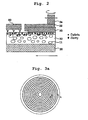
- a CMP method using the CMP machine 1 is schematically illustrated in Fig. 2 .
- the CMP method includes a chemical etching reaction process and a mechanical polishing process, which are conducted using a polishing pad 10 included in the CMP machine 1.
- the chemical etching reaction is carried out by a slurry 42. That is, the slurry 42 serves to chemically react with the surface of a wafer 30 to be polished, thereby making it possible for the mechanical polishing process, following the chemical etching reaction, to be easily carried out.
- the polishing pad 10 which is fixedly mounted on a platen 20, rotates.
- a slurry containing abrasive particles is supplied to the polishing pad 10 by a slurry supply means 40.
- the supplied slurry is introduced between the polishing pad 10 and the wafer 30.
- the introduced abrasive particles come into frictional contact with the wafer 30 by virtue of a relative rotating speed difference between the polishing pad 10 and the wafer 30, so that they conduct mechanical polishing.
- the slurry 42 is a colloidal liquid containing abrasive particles having a grain size of nanometers. This slurry 42 is spread on the polishing pad 10 during the polishing process.
- the polishing pad 10 rotates during the polishing process, the slurry 42 supplied to the polishing pad 10 is outwardly discharged from the periphery of the polishing pad 10 due to a centrifugal force caused by the rotation of the polishing pad 10.
- many abrasive particles should remain for a desirable lengthy period of time on the upper surface of the polishing pad 10 so that they participate in the polishing of the wafer. That is, the polishing pad 10 should make the slurry 42 be held on the surface thereof for as long a period of time as possible.
- Centrifugal force generated during the rotation of the CMP pad is higher at a position nearer to the periphery of the polishing pad. Due to such a centrifugal force difference between different radial positions on the polishing pad, the slurry on the polishing pad exhibits an increased flow rate as it approaches the periphery of the polishing pad. Thus, the slurry is non-uniformly distributed in the radial direction of the polishing pad. Due to such a non-uniform distribution of the slurry, the wafer is non-uniformly polished because its polishing rate is varied depending on a radial position of the polishing pad in contact with the wafer's surface. Such a variation in polishing rate affects the planarization of the wafer. As a result, The polishing pad exhibits a considerable difference in polishing rate between its central portion and its peripheral portion. For this reason, it is necessary to uniformly distribute the slurry over the polishing pad by controlling the flow of slurry on the polishing pad.
- the wafer is pressed against the polishing pad so that it comes into frictional contact with abrasive particles. Due to this pressure, however, it may be difficult for the slurry to reach the central.portion of the wafer. For this reason, the slurry may be distributed at the central portion of the wafer in a relatively reduced amount, as compared to the amount at the peripheral portion of the wafer. As a result, the wafer is non-uniformly polished.
- holes or grooves having a desired width, depth and shape are formed on a CMP pad. Such holes or grooves act to control the flow and distribution of the slurry continuously supplied during the polishing process.
- Fig. 3a is a schematic view illustrating a polishing pad formed with grooves respectively having the form of concentric circles.
- Fig. 3b is a cross-sectional view taken along the line A - A of Fig. 3a .
- the grooves formed on the polishing pad have the form of concentric circles uniformly spaced apart from one another in a radial direction while having different diameters, respectively.
- the slurry which is continuously supplied onto the polishing pad, is forced to move outwardly by a centrifugal force generated as the polishing pad rotates. As a result, during the polishing process, the slurry is temporarily collected in the concentric circular grooves, and then outwardly discharged from those grooves.
- concentric circular grooves An example of such concentric circular grooves is disclosed in U.S. Patent No. 5,984,769 and EP1066928 .
- EP1066928 also a polishing pad is disclosed that contains a plurality of concentric circular grooves and a plurality of concentric wave shaped grooves, the wave shaped grooves of different diameters each have a desired depth, desired width and desired shape.
- a polishing pad with only wave shaped grooves is disclosed to JP2001071256 .
- Fig. 4a is a schematic view illustrating a polishing pad formed with grooves having the form of a lattice.
- Fig. 4b is a cross-sectional view illustrating the lattice-shaped grooves of Fig. 4a .
- the polishing pad shown in Fig. 4a has a plurality of grooves extending an X axis and a plurality of grooves extending a Y axis while crossing the X-axis grooves to form a lattice.
- Such lattice-shaped grooves serve two collect a slurry continuously supplied onto the polishing pad, thereby retarding the discharge of the slurry caused by centrifugal force.
- the slurry supplied onto the polishing pad is hindered from flowing toward the central portion of a wafer being polished at regions where the polishing pad is in contact with the wafer. As a result, a degradation in polishing rate occurs at the central portion of the wafer.
- lattice-shaped grooves extend in an opened state to the periphery of the polishing pad without having any closed portion, the slurry supplied onto the polishing pad is easily discharged from the polishing pad. As a result, the lattice-shaped grooves cause an increased consumption of slurry, as compared to concentric circular grooves. It was also reported that holes cause increased consumption of slurry, as compared to lattice-shaped grooves, because those holes involve a reduction of the cross-sectional area capable of storing slurry. In the case of concentric circular grooves, a superior slurry storage capacity is obtained because each groove has a partially closed structure having vertical groove walls capable of retaining the slurry in the groove against centrifugal force, as compared to other structures. However, this structure has a drawback in that each groove has an insufficient depth corresponding to 1/4 of the thickness of the polishing pad.
- the conventional method which is used to form grooves at a polishing pad, utilize a cutting process conducted by a lathe or milling, the grooves have a fixed pattern such as concentric circles or a lattice. For this reason, it is difficult to form a groove pattern capable of effectively controlling the flow of a slurry.
- an object of the invention is to provide a CMP pad for a CMP process which is formed with wave-shaped grooves capable of retarding the discharge rate of a slurry supplied onto a polishing surface while uniformly distributing the slurry over the polishing surface.
- Another object of the invention is to provide a CMP pad formed with wave-shaped grooves capable of effectively controlling the flow of a slurry supplied onto the polishing pad during a CMP process.
- a CMP pad used for a CMP process, wherein a plurality of wave-shaped concentric grooves of different diameters each having a desired depth, a desired width and a desired shape are formed at a polishing surface of the pad.
- the CMP pad is divided into a plurality of radial regions having the same groove depths and the same groove width while each of the radial regions is different from the remaining radial regions in terms of groove depths and groove width.
- the concentric grooves are non-uniformly spaced apart from one another so that the groove space defined between ones adjacent to the concentric grooves is gradually reduced from a central portion of the pad to a peripheral portion of the pad, and the groove space are inversely proportional to an increase in the radius thereof.
- a CMP pad which has, at a polishing surface thereof, a plurality of wave-shaped concentric grooves of different diameters each having a desired depth, width and shape.
- the wave-shaped grooves of the present invention have the form of concentric sinusoidal loops each having a desired amplitude and a desired number of cycles.
- Various examples of such wave-shaped grooves are illustrated in Figs. 5 to 8 , respectively
- Such wave-shaped concentric grooves each having the form of a sinusoidal loop have diverse shapes in accordance with the number of cycles and amplitude of the sinusoidal loop.
- the wave-shaped concentric grooves may have an asteroid shape.
- the sinusoidal. loop has a number of cycles corresponding to 3 to 1,000.
- the shape of the grooves may be varied by adjusting the number of cycles and amplitude of the sinusoidal loop in accordance with the given polishing conditions. Referring to Figs.
- wave-shaped concentric grooves each having the form of a sinusoidal loop having a number of cycles corresponding to 12 are illustrated, respectively.
- Fig. 6 illustrates wave-shaped concentric grooves each having the form of a sinusoidal loop having a number of cycles corresponding to 6, respectively.
- each groove has a width of 10 ⁇ m to 10 mm.
- the space defined between adjacent ones of the grooves is preferable within a range of 10 ⁇ m to 100 mm.
- the wave-shaped concentric grooves formed on the polishing pad are non-uniformly spaced apart from one another.
- the groove space varies in accordance with the radius thereof.
- the polishing pad has at least two sets of grooves having different groove spaces in order to minimize the non-uniformity of the slurry caused by centrifugal force generated during a polishing process.
- the groove space is gradually reduced from the central portion to the peripheral portion of the polishing pad while being inversely proportional to an increase in the radius thereof.
- the polishing pad is divided into a plurality of radial regions.
- Each radial region may have a groove depth, groove width, or groove different from that of the remaining radial region.
- the polishing pad may be divided into inner and outer radial regions respectively defined at opposite sides of a circle having a radius r 0 .
- the inner radial region has a radius smaller than the radius r 0 (r ⁇ r 0 ) whereas the outer radial region has a radius larger than the radius r 0 (r > r 0 ).
- Each of the inner and outer radial regions has a uniform grooves space.
- the inner radial region may have a larger grooves space than that of the outer radial region.
- Concentric circles or lines each composed of holes, grooves, or a combination thereof may be additionally formed on the polishing pad formed with the above described wave-shaped concentric grooves.
- a polishing pad which has, at its polishing surface, a plurality of concentric circles of different diameters each composed of holes, in addition to the grooves shown in Fig. 5 .
- the space between adjacent ones of the concentric circles is non-uniform. Also, the circle space varies gradually in accordance with the radius thereof.
- a polishing pad which has, at its polishing surface, a plurality of concentric circles of different diameters each composed of holes and four diametrically-extending straight lines each composed of holes, in addition to the above described wave-shaped concentric holes.
- the straight lines formed on the polishing pad are symmetrical in a diametrical direction.
- the present invention provides a polishing pad formed with a plurality of wave-shaped concentric grooves of the same shape while having different diameters. It is possible to make the grooves with diverse patterns by varying the wave shape, groove width, groove depth or groove space.
- the pattern of the grooves may be further diversified where the polishing pad is additionally formed with a plurality of concentric circles or straight lines each composed of grooves, holes or a combination thereof.
- the groove space, width or depth at a portion of the polishing pad most frequently contacting the central portion of the wafer may also be adjusted.
- the formation of holes or grooves according to the present invention is achieved using a laser machining process.
- the laser machining process provides advantages in that it is capable of precisely machining holes or grooves having a complicates structure, making the holes or grooves with a smooth inner surface, and easily adjusting the shape, size, and depth of the holes or grooves.
- the polishing pad which is formed with a plurality of wave-shaped concentric grooves having the same shape while having different diameters in accordance with the present invention, is advantageous in that it can have diverse groove and hole patterns capable of optimally meeting the given polishing process conditions.
- the wave-shaped grooves of the polishing pad according to the present invention provides an increased area, through which a slurry passes before outwardly being discharged during a polishing process, as compared to grooves having the form of concentric circles. Accordingly, it is possible to retard the discharge rate of the slurry while uniformly distributing the slurry over the polishing surface, and effectively controlling the flow of the slurry during the polishing process, thereby maintaining a stable desired polishing rate and achieving an improved planarization.
Landscapes
- Engineering & Computer Science (AREA)
- Mechanical Engineering (AREA)
- Mechanical Treatment Of Semiconductor (AREA)
- Finish Polishing, Edge Sharpening, And Grinding By Specific Grinding Devices (AREA)
- Sampling And Sample Adjustment (AREA)
Abstract
Description
- The present invention relates to a polishing pad used in a chemical mechanical polishing process, and more particularly to a chemical mechanical polishing pad formed at a polishing surface thereof with a plurality of wave-shaped concentric grooves of different diameters each having a desired depth, width and shape.
- Generally, chemical mechanical polishing (CMP) is a high precision/mirrored surface polishing method used to obtain global planarization in a semiconductor device manufacturing process. In accordance with such CMP, a slurry is supplied between a polishing pad and a wafer to be polished, so as to chemically etch the surface of the wafer. Using the polishing pad, the etched surface of the wafer is mechanically polished.
- Referring to
Fig. 1 , a typical CMP machine, which is denoted by thereference numeral 1, is schematically illustrated. Also, a CMP method using theCMP machine 1 is schematically illustrated inFig. 2 . The CMP method includes a chemical etching reaction process and a mechanical polishing process, which are conducted using apolishing pad 10 included in theCMP machine 1. The chemical etching reaction is carried out by aslurry 42. That is, theslurry 42 serves to chemically react with the surface of awafer 30 to be polished, thereby making it possible for the mechanical polishing process, following the chemical etching reaction, to be easily carried out. In the mechanical polishing process, thepolishing pad 10, which is fixedly mounted on aplaten 20, rotates. Thewafer 30, which is firmly held by aretainer ring 32, rotates while oscillating. A slurry containing abrasive particles is supplied to thepolishing pad 10 by a slurry supply means 40. The supplied slurry is introduced between thepolishing pad 10 and thewafer 30. The introduced abrasive particles come into frictional contact with thewafer 30 by virtue of a relative rotating speed difference between thepolishing pad 10 and thewafer 30, so that they conduct mechanical polishing. Theslurry 42 is a colloidal liquid containing abrasive particles having a grain size of nanometers. Thisslurry 42 is spread on thepolishing pad 10 during the polishing process. As thepolishing pad 10 rotates during the polishing process, theslurry 42 supplied to thepolishing pad 10 is outwardly discharged from the periphery of thepolishing pad 10 due to a centrifugal force caused by the rotation of thepolishing pad 10. In order to achieve an enhanced polishing efficiency, many abrasive particles should remain for a desirable lengthy period of time on the upper surface of thepolishing pad 10 so that they participate in the polishing of the wafer. That is, thepolishing pad 10 should make theslurry 42 be held on the surface thereof for as long a period of time as possible. - Centrifugal force generated during the rotation of the CMP pad is higher at a position nearer to the periphery of the polishing pad. Due to such a centrifugal force difference between different radial positions on the polishing pad, the slurry on the polishing pad exhibits an increased flow rate as it approaches the periphery of the polishing pad. Thus, the slurry is non-uniformly distributed in the radial direction of the polishing pad. Due to such a non-uniform distribution of the slurry, the wafer is non-uniformly polished because its polishing rate is varied depending on a radial position of the polishing pad in contact with the wafer's surface. Such a variation in polishing rate affects the planarization of the wafer. As a result, The polishing pad exhibits a considerable difference in polishing rate between its central portion and its peripheral portion. For this reason, it is necessary to uniformly distribute the slurry over the polishing pad by controlling the flow of slurry on the polishing pad.
- During the polishing process, the wafer is pressed against the polishing pad so that it comes into frictional contact with abrasive particles. Due to this pressure, however, it may be difficult for the slurry to reach the central.portion of the wafer. For this reason, the slurry may be distributed at the central portion of the wafer in a relatively reduced amount, as compared to the amount at the peripheral portion of the wafer. As a result, the wafer is non-uniformly polished.
- In order to solve such a problem, a method has been proposed, in which holes or grooves having a desired width, depth and shape are formed on a CMP pad. Such holes or grooves act to control the flow and distribution of the slurry continuously supplied during the polishing process.
- Now, holes or grooves conventionally formed on a polishing pad will be described in conjunction with the annexed drawings.
-
Fig. 3a is a schematic view illustrating a polishing pad formed with grooves respectively having the form of concentric circles.Fig. 3b is a cross-sectional view taken along the line A - A ofFig. 3a . As shown inFigs. 3a and3b , the grooves formed on the polishing pad have the form of concentric circles uniformly spaced apart from one another in a radial direction while having different diameters, respectively. The slurry, which is continuously supplied onto the polishing pad, is forced to move outwardly by a centrifugal force generated as the polishing pad rotates. As a result, during the polishing process, the slurry is temporarily collected in the concentric circular grooves, and then outwardly discharged from those grooves. An example of such concentric circular grooves is disclosed inU.S. Patent No. 5,984,769 andEP1066928 . InEP1066928 also a polishing pad is disclosed that contains a plurality of concentric circular grooves and a plurality of concentric wave shaped grooves, the wave shaped grooves of different diameters each have a desired depth, desired width and desired shape. A polishing pad with only wave shaped grooves is disclosed toJP2001071256 -
Fig. 4a is a schematic view illustrating a polishing pad formed with grooves having the form of a lattice.Fig. 4b is a cross-sectional view illustrating the lattice-shaped grooves ofFig. 4a . The polishing pad shown inFig. 4a has a plurality of grooves extending an X axis and a plurality of grooves extending a Y axis while crossing the X-axis grooves to form a lattice. Such lattice-shaped grooves serve two collect a slurry continuously supplied onto the polishing pad, thereby retarding the discharge of the slurry caused by centrifugal force. - In the case of the conventional polishing pad having grooves uniformly spaced apart from one another, the slurry supplied onto the polishing pad is hindered from flowing toward the central portion of a wafer being polished at regions where the polishing pad is in contact with the wafer. As a result, a degradation in polishing rate occurs at the central portion of the wafer.
- Since lattice-shaped grooves extend in an opened state to the periphery of the polishing pad without having any closed portion, the slurry supplied onto the polishing pad is easily discharged from the polishing pad. As a result, the lattice-shaped grooves cause an increased consumption of slurry, as compared to concentric circular grooves. It was also reported that holes cause increased consumption of slurry, as compared to lattice-shaped grooves, because those holes involve a reduction of the cross-sectional area capable of storing slurry. In the case of concentric circular grooves, a superior slurry storage capacity is obtained because each groove has a partially closed structure having vertical groove walls capable of retaining the slurry in the groove against centrifugal force, as compared to other structures. However, this structure has a drawback in that each groove has an insufficient depth corresponding to 1/4 of the thickness of the polishing pad.
- Since the conventional method, which is used to form grooves at a polishing pad, utilize a cutting process conducted by a lathe or milling, the grooves have a fixed pattern such as concentric circles or a lattice. For this reason, it is difficult to form a groove pattern capable of effectively controlling the flow of a slurry.
- In order to solve such a problem, it is necessary to design the shape, density and distribution of grooves, taking into consideration given polishing process conditions such as centrifugal force and wafer position.
- Therefore, an object of the invention is to provide a CMP pad for a CMP process which is formed with wave-shaped grooves capable of retarding the discharge rate of a slurry supplied onto a polishing surface while uniformly distributing the slurry over the polishing surface.
- Another object of the invention is to provide a CMP pad formed with wave-shaped grooves capable of effectively controlling the flow of a slurry supplied onto the polishing pad during a CMP process.
- In accordance with the present invention, these objects are accomplished by providing a CMP pad used for a CMP process, wherein a plurality of wave-shaped concentric grooves of different diameters each having a desired depth, a desired width and a desired shape are formed at a polishing surface of the pad. The CMP pad is divided into a plurality of radial regions having the same groove depths and the same groove width while each of the radial regions is different from the remaining radial regions in terms of groove depths and groove width.
The concentric grooves are non-uniformly spaced apart from one another so that the groove space defined between ones adjacent to the concentric grooves is gradually reduced from a central portion of the pad to a peripheral portion of the pad, and the groove space are inversely proportional to an increase in the radius thereof. -
-
Fig. 1 is a schematic view illustrating the configuration of a atypical CAMP machine and a polishing method performed using the CMP machine; -
Fig. 2 is a schematic view illustrating the concept of a CMP method; -
Fig. 3a is a schematic view illustrating a polishing pad formed with grooves respectively having the form of concentric circles; -
Fig. 3b is a crcss-sectional view taken along the line A - A ofFig. 3a ; -
Fig. 4a is a schematic view illustrating a polishing pad formed with lattice-shaped grooves having a conventional structure; -
Fig. 4b is a cross-sectional view illustrating the lattice-shaped grooves shown inFig. 4a ; -
Figs. 5 and6 are schematic views respectively illustrating polishing pads each formed with a plurality of wave-shaped concentric grooves having the same shape while having different diameters and being divided into two radial regions having different groove spaces in accordance with the present invention; -
Fig. 7 is a schematic view illustrating the polishing pad ofFig. 5 further formed with a plurality of concentric circles of different diameters each composed of holes; and -
Fig. 8 is a schematic view illustrating a polishing pad formed with a plurality of wave-shaped concentric grooves while being further formed with a plurality of concentric circles of different diameters and diametrical straight lines. - Now, the present invention will be described in detail in terms of its constitution and function, with reference to the annexed drawings.
- In accordance with the present invention, a CMP pad is provided which has, at a polishing surface thereof, a plurality of wave-shaped concentric grooves of different diameters each having a desired depth, width and shape.
- The wave-shaped grooves of the present invention have the form of concentric sinusoidal loops each having a desired amplitude and a desired number of cycles. Various examples of such wave-shaped grooves are illustrated in
Figs. 5 to 8 , respectively Such wave-shaped concentric grooves each having the form of a sinusoidal loop have diverse shapes in accordance with the number of cycles and amplitude of the sinusoidal loop. For example, the wave-shaped concentric grooves may have an asteroid shape. Preferably, the sinusoidal. loop has a number of cycles corresponding to 3 to 1,000. The shape of the grooves may be varied by adjusting the number of cycles and amplitude of the sinusoidal loop in accordance with the given polishing conditions. Referring toFigs. 5 and7 , wave-shaped concentric grooves each having the form of a sinusoidal loop having a number of cycles corresponding to 12 are illustrated, respectively. Also,Fig. 6 illustrates wave-shaped concentric grooves each having the form of a sinusoidal loop having a number of cycles corresponding to 6, respectively. - Such concentric grooves, which have the same wave shape, are formed on a polishing pad while being spaced apart from one another in accordance with the present invention. Preferably, each groove has a width of 10 µm to 10 mm. Also, the space defined between adjacent ones of the grooves is preferable within a range of 10 µm to 100 mm.
- The wave-shaped concentric grooves formed on the polishing pad are non-uniformly spaced apart from one another.
- According to present invention the groove space varies in accordance with the radius thereof. The polishing pad has at least two sets of grooves having different groove spaces in order to minimize the non-uniformity of the slurry caused by centrifugal force generated during a polishing process.
- According to present invention the groove space is gradually reduced from the central portion to the peripheral portion of the polishing pad while being inversely proportional to an increase in the radius thereof.
- In accordance with the present invention, the polishing pad is divided into a plurality of radial regions. Each radial region may have a groove depth, groove width, or groove different from that of the remaining radial region.
- As shown in
Fig. 5 , the polishing pad may be divided into inner and outer radial regions respectively defined at opposite sides of a circle having a radius r0. The inner radial region has a radius smaller than the radius r0 (r < r0) whereas the outer radial region has a radius larger than the radius r0 (r > r0). Each of the inner and outer radial regions has a uniform grooves space. Also, the inner radial region may have a larger grooves space than that of the outer radial region. - Concentric circles or lines each composed of holes, grooves, or a combination thereof may be additionally formed on the polishing pad formed with the above described wave-shaped concentric grooves.
- Referring to
Fig. 7 , a polishing pad is illustrated which has, at its polishing surface, a plurality of concentric circles of different diameters each composed of holes, in addition to the grooves shown inFig. 5 . The space between adjacent ones of the concentric circles is non-uniform. Also, the circle space varies gradually in accordance with the radius thereof. - Referring to
Fig. 8 , a polishing pad is illustrated which has, at its polishing surface, a plurality of concentric circles of different diameters each composed of holes and four diametrically-extending straight lines each composed of holes, in addition to the above described wave-shaped concentric holes. Preferably, the straight lines formed on the polishing pad are symmetrical in a diametrical direction. Of course, it is possible to form straight lines in the form of a lattice or oblique lines. - As apparent from the above description, the present invention provides a polishing pad formed with a plurality of wave-shaped concentric grooves of the same shape while having different diameters. It is possible to make the grooves with diverse patterns by varying the wave shape, groove width, groove depth or groove space. The pattern of the grooves may be further diversified where the polishing pad is additionally formed with a plurality of concentric circles or straight lines each composed of grooves, holes or a combination thereof.
- In order to allow the slurry to easily approach the central portion of the wafer during the polishing process, the groove space, width or depth at a portion of the polishing pad most frequently contacting the central portion of the wafer may also be adjusted.
- Preferably, the formation of holes or grooves according to the present invention is achieved using a laser machining process. The laser machining process provides advantages in that it is capable of precisely machining holes or grooves having a complicates structure, making the holes or grooves with a smooth inner surface, and easily adjusting the shape, size, and depth of the holes or grooves.
- The polishing pad, which is formed with a plurality of wave-shaped concentric grooves having the same shape while having different diameters in accordance with the present invention, is advantageous in that it can have diverse groove and hole patterns capable of optimally meeting the given polishing process conditions.
- The wave-shaped grooves of the polishing pad according to the present invention provides an increased area, through which a slurry passes before outwardly being discharged during a polishing process, as compared to grooves having the form of concentric circles. Accordingly, it is possible to retard the discharge rate of the slurry while uniformly distributing the slurry over the polishing surface, and effectively controlling the flow of the slurry during the polishing process, thereby maintaining a stable desired polishing rate and achieving an improved planarization.
- Although the preferred embodiments of the invention have been disclosed for illustrative purposes in conjunction with a polishing pad having wave-shaped grooves, those skilled in the art will appreciate that various modifications, additions and substitutions are possible, without departing from the scope of the invention as disclosed in the accompanying claims.
Claims (11)
- A chemical mechanical polishing pad (10) used for a chemical mechanical polishing process, which is divided into a plurality of radial regions formed with the wave-shaped concentric grooves having a desired groove depth and a desired groove width, characterized in that
the concentric grooves have a form of a sinusoidal loop having a number of cycles corresponding to 3 to 1000,
the grooves of each of the radial regions having the same groove depth and the same groove width while each of the radial regions being different from the remaining radial regions in terms of groove depth and groove width,
and the concentric grooves are non-uniformly spaced apart from one another so that the groove space defined between ones adjacent to the concentric grooves is gradually reduced from a central portion of the pad to a peripheral portion of the pad (10),
and the groove space being inversely proportional to an increase in the radius thereof. - The chemical mechanical polishing pad (10) according to claim 1, wherein each of the wave-shaped concentric grooves has a width of 10 µm to 10 mm.
- The chemical mechanical polishing pad (10) according to claim 1, wherein the wave-shaped concentric grooves are spaced apart from one another, so as to have a groove space of 10 µm to 100 mm.
- The chemical mechanical polishing pad (10) according to any one of claims 1 to 3, wherein a plurality of concentric circles each composed of grooves,
holes or a combination thereof are further formed at the polishing surface. - The chemical mechanical polishing pad (10) according to claim 4, wherein the concentric circles are spaced apart from on another so that they are grouped into at least two sets having different groove spaces.
- The chemical mechanical polishing pad (10) according to claim 4, wherein the concentric circles are spaced apart from one another so that the circle space defined between adjacent ones of the concentric circles is gradually reduced from a central portion of the pad to a peripheral portion of the pad.
- The chemical mechanical polishing pad (10) according to any one of claims 1 to 3, wherein one or more straight lines each composed of grooves, holes or a combination thereof are further formed at the polishing pad.
- The chemical mechanical polishing pad (10) according to claim 7, wherein the straight lines are grouped into a group of horizontal straight lines spaced apart from one another and a group of vertical straight lines spaced apart from one another while crossing the horizontal straight lines to form a lattice structure.
- The chemical mechanical polishing pad (10) according to claim 7, wherein the straight lines cross together at a center of the polishing surface so that they are symmetrically arranged in a diametrical direction.
- The chemical mechanical polishing pad (10) according to any one of claims 1 to 3, wherein a plurality of concentric circles each composed of grooves, holes or a combination thereof and one or more straight lines each composed of grooves, holes or a combination thereof are further formed at the polishing surface.
- The chemical mechanical polishing pad (10) according to any one of claims 1 to 3, wherein the wave-shaped grooves are machined by a laser.
Applications Claiming Priority (3)
| Application Number | Priority Date | Filing Date | Title |
|---|---|---|---|
| KR2001049354 | 2001-08-16 | ||
| KR1020010049354A KR20030015567A (en) | 2001-08-16 | 2001-08-16 | Chemical mechanical polishing pad having wave grooves |
| PCT/KR2001/001464 WO2003017347A1 (en) | 2001-08-16 | 2001-08-29 | Chemical mechanical polishing pad having wave-shaped grooves |
Publications (3)
| Publication Number | Publication Date |
|---|---|
| EP1433197A1 EP1433197A1 (en) | 2004-06-30 |
| EP1433197A4 EP1433197A4 (en) | 2008-04-09 |
| EP1433197B1 true EP1433197B1 (en) | 2011-04-20 |
Family
ID=19713250
Family Applications (1)
| Application Number | Title | Priority Date | Filing Date |
|---|---|---|---|
| EP01965710A Expired - Lifetime EP1433197B1 (en) | 2001-08-16 | 2001-08-29 | Chemical mechanical polishing pad having wave-shaped grooves |
Country Status (9)
| Country | Link |
|---|---|
| US (1) | US6729950B2 (en) |
| EP (1) | EP1433197B1 (en) |
| JP (1) | JP2005500689A (en) |
| KR (1) | KR20030015567A (en) |
| CN (1) | CN1284210C (en) |
| AT (1) | ATE506695T1 (en) |
| DE (1) | DE60144494D1 (en) |
| TW (1) | TW504429B (en) |
| WO (1) | WO2003017347A1 (en) |
Families Citing this family (62)
| Publication number | Priority date | Publication date | Assignee | Title |
|---|---|---|---|---|
| US7374644B2 (en) * | 2000-02-17 | 2008-05-20 | Applied Materials, Inc. | Conductive polishing article for electrochemical mechanical polishing |
| US20080156657A1 (en) * | 2000-02-17 | 2008-07-03 | Butterfield Paul D | Conductive polishing article for electrochemical mechanical polishing |
| US7077721B2 (en) * | 2000-02-17 | 2006-07-18 | Applied Materials, Inc. | Pad assembly for electrochemical mechanical processing |
| US7059948B2 (en) * | 2000-12-22 | 2006-06-13 | Applied Materials | Articles for polishing semiconductor substrates |
| US7125477B2 (en) * | 2000-02-17 | 2006-10-24 | Applied Materials, Inc. | Contacts for electrochemical processing |
| US7303462B2 (en) * | 2000-02-17 | 2007-12-04 | Applied Materials, Inc. | Edge bead removal by an electro polishing process |
| US6979248B2 (en) * | 2002-05-07 | 2005-12-27 | Applied Materials, Inc. | Conductive polishing article for electrochemical mechanical polishing |
| US7029365B2 (en) | 2000-02-17 | 2006-04-18 | Applied Materials Inc. | Pad assembly for electrochemical mechanical processing |
| US20040020789A1 (en) * | 2000-02-17 | 2004-02-05 | Applied Materials, Inc. | Conductive polishing article for electrochemical mechanical polishing |
| US6962524B2 (en) * | 2000-02-17 | 2005-11-08 | Applied Materials, Inc. | Conductive polishing article for electrochemical mechanical polishing |
| US6991528B2 (en) * | 2000-02-17 | 2006-01-31 | Applied Materials, Inc. | Conductive polishing article for electrochemical mechanical polishing |
| US7066800B2 (en) * | 2000-02-17 | 2006-06-27 | Applied Materials Inc. | Conductive polishing article for electrochemical mechanical polishing |
| US20050092621A1 (en) * | 2000-02-17 | 2005-05-05 | Yongqi Hu | Composite pad assembly for electrochemical mechanical processing (ECMP) |
| US7670468B2 (en) * | 2000-02-17 | 2010-03-02 | Applied Materials, Inc. | Contact assembly and method for electrochemical mechanical processing |
| US7303662B2 (en) * | 2000-02-17 | 2007-12-04 | Applied Materials, Inc. | Contacts for electrochemical processing |
| US7678245B2 (en) * | 2000-02-17 | 2010-03-16 | Applied Materials, Inc. | Method and apparatus for electrochemical mechanical processing |
| US8485862B2 (en) * | 2000-05-19 | 2013-07-16 | Applied Materials, Inc. | Polishing pad for endpoint detection and related methods |
| US7137879B2 (en) * | 2001-04-24 | 2006-11-21 | Applied Materials, Inc. | Conductive polishing article for electrochemical mechanical polishing |
| US7344432B2 (en) * | 2001-04-24 | 2008-03-18 | Applied Materials, Inc. | Conductive pad with ion exchange membrane for electrochemical mechanical polishing |
| US20030072639A1 (en) * | 2001-10-17 | 2003-04-17 | Applied Materials, Inc. | Substrate support |
| JP3843933B2 (en) * | 2002-02-07 | 2006-11-08 | ソニー株式会社 | Polishing pad, polishing apparatus and polishing method |
| US20050194681A1 (en) * | 2002-05-07 | 2005-09-08 | Yongqi Hu | Conductive pad with high abrasion |
| TWI250572B (en) * | 2002-06-03 | 2006-03-01 | Jsr Corp | Polishing pad and multi-layer polishing pad |
| US6942549B2 (en) * | 2003-10-29 | 2005-09-13 | International Business Machines Corporation | Two-sided chemical mechanical polishing pad for semiconductor processing |
| US7018274B2 (en) * | 2003-11-13 | 2006-03-28 | Rohm And Haas Electronic Materials Cmp Holdings, Inc | Polishing pad having slurry utilization enhancing grooves |
| US7125318B2 (en) * | 2003-11-13 | 2006-10-24 | Rohm And Haas Electronic Materials Cmp Holdings, Inc. | Polishing pad having a groove arrangement for reducing slurry consumption |
| JP2005177897A (en) * | 2003-12-17 | 2005-07-07 | Nec Electronics Corp | Polishing method, polishing device, and method of manufacturing semiconductor device |
| US20050178666A1 (en) * | 2004-01-13 | 2005-08-18 | Applied Materials, Inc. | Methods for fabrication of a polishing article |
| US6955587B2 (en) * | 2004-01-30 | 2005-10-18 | Rohm And Haas Electronic Materials Cmp Holdings, Inc | Grooved polishing pad and method |
| US6958002B1 (en) * | 2004-07-19 | 2005-10-25 | Rohm And Haas Electronic Materials Cmp Holdings, Inc. | Polishing pad with flow modifying groove network |
| US20060030156A1 (en) * | 2004-08-05 | 2006-02-09 | Applied Materials, Inc. | Abrasive conductive polishing article for electrochemical mechanical polishing |
| US7252582B2 (en) * | 2004-08-25 | 2007-08-07 | Jh Rhodes Company, Inc. | Optimized grooving structure for a CMP polishing pad |
| US7084064B2 (en) * | 2004-09-14 | 2006-08-01 | Applied Materials, Inc. | Full sequence metal and barrier layer electrochemical mechanical processing |
| WO2006039436A2 (en) * | 2004-10-01 | 2006-04-13 | Applied Materials, Inc. | Pad design for electrochemical mechanical polishing |
| US7520968B2 (en) * | 2004-10-05 | 2009-04-21 | Applied Materials, Inc. | Conductive pad design modification for better wafer-pad contact |
| US7131895B2 (en) * | 2005-01-13 | 2006-11-07 | Rohm And Haas Electronic Materials Cmp Holdings, Inc. | CMP pad having a radially alternating groove segment configuration |
| TWI385050B (en) * | 2005-02-18 | 2013-02-11 | 奈平科技股份有限公司 | Special polishing pad for CMP, its manufacturing method and use thereof |
| US20060219663A1 (en) * | 2005-03-31 | 2006-10-05 | Applied Materials, Inc. | Metal CMP process on one or more polishing stations using slurries with oxidizers |
| US7427340B2 (en) * | 2005-04-08 | 2008-09-23 | Applied Materials, Inc. | Conductive pad |
| JP2007030157A (en) * | 2005-06-20 | 2007-02-08 | Elpida Memory Inc | Polishing device and method |
| KR100752181B1 (en) * | 2005-10-05 | 2007-08-24 | 동부일렉트로닉스 주식회사 | Chemical mechanical polishing machine |
| KR20070070094A (en) * | 2005-12-28 | 2007-07-03 | 제이에스알 가부시끼가이샤 | Chemical mechanical polishing pad and chemical mechanical polishing method |
| US20080003935A1 (en) * | 2006-07-03 | 2008-01-03 | Chung-Chih Feng | Polishing pad having surface texture |
| US20080220702A1 (en) * | 2006-07-03 | 2008-09-11 | Sang Fang Chemical Industry Co., Ltd. | Polishing pad having surface texture |
| US7267610B1 (en) * | 2006-08-30 | 2007-09-11 | Rohm And Haas Electronic Materials Cmp Holdings, Inc. | CMP pad having unevenly spaced grooves |
| US8002611B2 (en) * | 2006-12-27 | 2011-08-23 | Texas Instruments Incorporated | Chemical mechanical polishing pad having improved groove pattern |
| US20080293343A1 (en) * | 2007-05-22 | 2008-11-27 | Yuchun Wang | Pad with shallow cells for electrochemical mechanical processing |
| US9180570B2 (en) * | 2008-03-14 | 2015-11-10 | Nexplanar Corporation | Grooved CMP pad |
| KR101004256B1 (en) | 2008-03-20 | 2011-01-03 | 엠.씨.케이 (주) | Polishing pad and manufacturing method thereof |
| TWI449597B (en) * | 2008-07-09 | 2014-08-21 | Iv Technologies Co Ltd | Polishing pad and method of forming the same |
| TWI535527B (en) * | 2009-07-20 | 2016-06-01 | 智勝科技股份有限公司 | Polishing method, polishing pad and polishing system |
| KR101044281B1 (en) * | 2009-07-30 | 2011-06-28 | 서강대학교산학협력단 | CPM polishing pad with pores formed therein and a method of manufacturing the same |
| CN103109355B (en) * | 2010-09-15 | 2016-07-06 | 株式会社Lg化学 | Abrasive pads for CMP |
| EP2546105B1 (en) | 2011-07-14 | 2014-05-21 | LG Electronics Inc. | Holding apparatus for portable electronic device |
| KR101295921B1 (en) * | 2011-11-07 | 2013-08-13 | 주식회사 엘지실트론 | Surface treatment method of polishing pad and polishing method of wafer using the same |
| CN103372812A (en) * | 2013-07-12 | 2013-10-30 | 中国科学院上海光学精密机械研究所 | Slotting device for polishing plastic disc of large ring polishing machine |
| US9849562B2 (en) | 2015-12-28 | 2017-12-26 | Shine-File Llc | And manufacture of an abrasive polishing tool |
| CN105619202A (en) * | 2016-02-26 | 2016-06-01 | 上海华力微电子有限公司 | Chemical mechanical grinding device and chemical mechanical grinding method thereof |
| TWI595968B (en) * | 2016-08-11 | 2017-08-21 | 宋建宏 | Polishing pad and method for manufacturing the same |
| CN110842764A (en) * | 2019-11-18 | 2020-02-28 | 张俊杰 | A grinding disc device for the development of superhard ceramic spherical parts |
| GB2590511B (en) * | 2019-11-20 | 2023-10-25 | Best Engineered Surface Tech Llc | Hybrid CMP conditioning head |
| CN113153380B (en) * | 2021-05-18 | 2022-04-26 | 中铁第四勘察设计院集团有限公司 | Method for improving waterproof performance of pipe sheet joint in shield tunnel |
Family Cites Families (23)
| Publication number | Priority date | Publication date | Assignee | Title |
|---|---|---|---|---|
| JPS60109859U (en) * | 1983-12-28 | 1985-07-25 | 株式会社 デイスコ | Semiconductor wafer surface grinding equipment |
| US5177908A (en) * | 1990-01-22 | 1993-01-12 | Micron Technology, Inc. | Polishing pad |
| US5329734A (en) * | 1993-04-30 | 1994-07-19 | Motorola, Inc. | Polishing pads used to chemical-mechanical polish a semiconductor substrate |
| JPH0752033A (en) * | 1993-08-06 | 1995-02-28 | Sumitomo Metal Ind Ltd | Polishing equipment |
| US5650039A (en) * | 1994-03-02 | 1997-07-22 | Applied Materials, Inc. | Chemical mechanical polishing apparatus with improved slurry distribution |
| JP3042593B2 (en) * | 1995-10-25 | 2000-05-15 | 日本電気株式会社 | Polishing pad |
| JP2865061B2 (en) * | 1996-06-27 | 1999-03-08 | 日本電気株式会社 | Polishing pad, polishing apparatus, and semiconductor device manufacturing method |
| US5645469A (en) * | 1996-09-06 | 1997-07-08 | Advanced Micro Devices, Inc. | Polishing pad with radially extending tapered channels |
| US6273806B1 (en) * | 1997-05-15 | 2001-08-14 | Applied Materials, Inc. | Polishing pad having a grooved pattern for use in a chemical mechanical polishing apparatus |
| US5921855A (en) * | 1997-05-15 | 1999-07-13 | Applied Materials, Inc. | Polishing pad having a grooved pattern for use in a chemical mechanical polishing system |
| JPH11285962A (en) * | 1998-04-06 | 1999-10-19 | Sony Corp | Polishing pad, polishing apparatus and polishing method |
| JP3920465B2 (en) * | 1998-08-04 | 2007-05-30 | 信越半導体株式会社 | Polishing method and polishing apparatus |
| GB2345255B (en) * | 1998-12-29 | 2000-12-27 | United Microelectronics Corp | Chemical-Mechanical Polishing Pad |
| US6220942B1 (en) * | 1999-04-02 | 2001-04-24 | Applied Materials, Inc. | CMP platen with patterned surface |
| US6238271B1 (en) * | 1999-04-30 | 2001-05-29 | Speed Fam-Ipec Corp. | Methods and apparatus for improved polishing of workpieces |
| US6261168B1 (en) * | 1999-05-21 | 2001-07-17 | Lam Research Corporation | Chemical mechanical planarization or polishing pad with sections having varied groove patterns |
| KR20010002470A (en) * | 1999-06-15 | 2001-01-15 | 고석태 | groove-pattern of polishing pad for chemical-mechanical polishing equipment |
| JP2001071256A (en) * | 1999-08-31 | 2001-03-21 | Shinozaki Seisakusho:Kk | Polishing pad groove forming method and apparatus, and polishing pad |
| KR100348525B1 (en) * | 1999-10-09 | 2002-08-14 | 동성에이앤티 주식회사 | Polishing pad with various groove-pattern |
| JP2001179611A (en) * | 1999-12-24 | 2001-07-03 | Nec Corp | Chemical machine polishing device |
| US6241596B1 (en) * | 2000-01-14 | 2001-06-05 | Applied Materials, Inc. | Method and apparatus for chemical mechanical polishing using a patterned pad |
| US6443815B1 (en) * | 2000-09-22 | 2002-09-03 | Lam Research Corporation | Apparatus and methods for controlling pad conditioning head tilt for chemical mechanical polishing |
| CN1328009C (en) * | 2001-08-02 | 2007-07-25 | 株式会社Skc | Method for fabricating chemical mechanical polishing pad using laser |
-
2001
- 2001-08-16 KR KR1020010049354A patent/KR20030015567A/en not_active Ceased
- 2001-08-29 AT AT01965710T patent/ATE506695T1/en not_active IP Right Cessation
- 2001-08-29 JP JP2003522156A patent/JP2005500689A/en active Pending
- 2001-08-29 US US10/129,386 patent/US6729950B2/en not_active Expired - Lifetime
- 2001-08-29 WO PCT/KR2001/001464 patent/WO2003017347A1/en not_active Ceased
- 2001-08-29 CN CNB018235417A patent/CN1284210C/en not_active Expired - Lifetime
- 2001-08-29 DE DE60144494T patent/DE60144494D1/en not_active Expired - Lifetime
- 2001-08-29 EP EP01965710A patent/EP1433197B1/en not_active Expired - Lifetime
- 2001-10-15 TW TW090125420A patent/TW504429B/en not_active IP Right Cessation
Also Published As
| Publication number | Publication date |
|---|---|
| KR20030015567A (en) | 2003-02-25 |
| EP1433197A4 (en) | 2008-04-09 |
| ATE506695T1 (en) | 2011-05-15 |
| CN1284210C (en) | 2006-11-08 |
| JP2005500689A (en) | 2005-01-06 |
| WO2003017347A1 (en) | 2003-02-27 |
| US20030034131A1 (en) | 2003-02-20 |
| US6729950B2 (en) | 2004-05-04 |
| TW504429B (en) | 2002-10-01 |
| DE60144494D1 (en) | 2011-06-01 |
| EP1433197A1 (en) | 2004-06-30 |
| CN1543670A (en) | 2004-11-03 |
Similar Documents
| Publication | Publication Date | Title |
|---|---|---|
| US6729950B2 (en) | Chemical mechanical polishing pad having wave shaped grooves | |
| EP1417703B1 (en) | Chemical mechanical polishing pad having holes and/or grooves | |
| US6165904A (en) | Polishing pad for use in the chemical/mechanical polishing of a semiconductor substrate and method of polishing the substrate using the pad | |
| US8057282B2 (en) | High-rate polishing method | |
| US8062103B2 (en) | High-rate groove pattern | |
| US5882251A (en) | Chemical mechanical polishing pad slurry distribution grooves | |
| US6955587B2 (en) | Grooved polishing pad and method | |
| US6273806B1 (en) | Polishing pad having a grooved pattern for use in a chemical mechanical polishing apparatus | |
| CN112959212B (en) | Chemical mechanical polishing pad with optimized grooves and application thereof | |
| US6974372B1 (en) | Polishing pad having grooves configured to promote mixing wakes during polishing | |
| EP1430520B1 (en) | Chemical mechanical polishing pad with micro-holes | |
| KR100597710B1 (en) | Chemical Mechanical Polishing Pads with Wave Grooves | |
| KR100636431B1 (en) | Chemical Mechanical Polishing Pads with Wave Grooves | |
| KR20010036591A (en) | Polishing pad with various groove-pattern | |
| KR200357678Y1 (en) | Polishing pad to CMP | |
| KR20010002470A (en) | groove-pattern of polishing pad for chemical-mechanical polishing equipment | |
| KR100652360B1 (en) | Chemical mechanical polishing apparatus with pad | |
| KR102832719B1 (en) | Polishing pad including protruding pattern with vertical groove, method for preparing the same, and polishing apparatus | |
| KR20010002467A (en) | groove-pattern of polishing pad for chemical-mechanical polishing equipment | |
| CN120572458A (en) | A chemical mechanical polishing pad with improved service life and its processing method and application | |
| KR20010002469A (en) | groove of polishing pad for chemical-mechanical polishing equipment |
Legal Events
| Date | Code | Title | Description |
|---|---|---|---|
| PUAI | Public reference made under article 153(3) epc to a published international application that has entered the european phase |
Free format text: ORIGINAL CODE: 0009012 |
|
| 17P | Request for examination filed |
Effective date: 20040213 |
|
| AK | Designated contracting states |
Kind code of ref document: A1 Designated state(s): AT BE CH CY DE DK ES FI FR GB GR IE IT LI LU MC NL PT SE TR |
|
| AX | Request for extension of the european patent |
Extension state: AL LT LV MK RO SI |
|
| A4 | Supplementary search report drawn up and despatched |
Effective date: 20080311 |
|
| RIC1 | Information provided on ipc code assigned before grant |
Ipc: B24B 37/04 20060101ALI20080305BHEP Ipc: H01L 21/304 20060101AFI20030305BHEP Ipc: B24D 13/14 20060101ALI20080305BHEP |
|
| 17Q | First examination report despatched |
Effective date: 20080620 |
|
| GRAP | Despatch of communication of intention to grant a patent |
Free format text: ORIGINAL CODE: EPIDOSNIGR1 |
|
| GRAS | Grant fee paid |
Free format text: ORIGINAL CODE: EPIDOSNIGR3 |
|
| GRAA | (expected) grant |
Free format text: ORIGINAL CODE: 0009210 |
|
| AK | Designated contracting states |
Kind code of ref document: B1 Designated state(s): AT BE CH CY DE DK ES FI FR GB GR IE IT LI LU MC NL PT SE TR |
|
| REG | Reference to a national code |
Ref country code: GB Ref legal event code: FG4D |
|
| REG | Reference to a national code |
Ref country code: CH Ref legal event code: EP |
|
| REG | Reference to a national code |
Ref country code: IE Ref legal event code: FG4D |
|
| REF | Corresponds to: |
Ref document number: 60144494 Country of ref document: DE Date of ref document: 20110601 Kind code of ref document: P |
|
| REG | Reference to a national code |
Ref country code: DE Ref legal event code: R096 Ref document number: 60144494 Country of ref document: DE Effective date: 20110601 |
|
| REG | Reference to a national code |
Ref country code: NL Ref legal event code: VDEP Effective date: 20110420 |
|
| PG25 | Lapsed in a contracting state [announced via postgrant information from national office to epo] |
Ref country code: SE Free format text: LAPSE BECAUSE OF FAILURE TO SUBMIT A TRANSLATION OF THE DESCRIPTION OR TO PAY THE FEE WITHIN THE PRESCRIBED TIME-LIMIT Effective date: 20110420 Ref country code: PT Free format text: LAPSE BECAUSE OF FAILURE TO SUBMIT A TRANSLATION OF THE DESCRIPTION OR TO PAY THE FEE WITHIN THE PRESCRIBED TIME-LIMIT Effective date: 20110822 |
|
| PG25 | Lapsed in a contracting state [announced via postgrant information from national office to epo] |
Ref country code: GR Free format text: LAPSE BECAUSE OF FAILURE TO SUBMIT A TRANSLATION OF THE DESCRIPTION OR TO PAY THE FEE WITHIN THE PRESCRIBED TIME-LIMIT Effective date: 20110721 Ref country code: FI Free format text: LAPSE BECAUSE OF FAILURE TO SUBMIT A TRANSLATION OF THE DESCRIPTION OR TO PAY THE FEE WITHIN THE PRESCRIBED TIME-LIMIT Effective date: 20110420 Ref country code: BE Free format text: LAPSE BECAUSE OF FAILURE TO SUBMIT A TRANSLATION OF THE DESCRIPTION OR TO PAY THE FEE WITHIN THE PRESCRIBED TIME-LIMIT Effective date: 20110420 Ref country code: ES Free format text: LAPSE BECAUSE OF FAILURE TO SUBMIT A TRANSLATION OF THE DESCRIPTION OR TO PAY THE FEE WITHIN THE PRESCRIBED TIME-LIMIT Effective date: 20110731 Ref country code: AT Free format text: LAPSE BECAUSE OF FAILURE TO SUBMIT A TRANSLATION OF THE DESCRIPTION OR TO PAY THE FEE WITHIN THE PRESCRIBED TIME-LIMIT Effective date: 20110420 Ref country code: CY Free format text: LAPSE BECAUSE OF FAILURE TO SUBMIT A TRANSLATION OF THE DESCRIPTION OR TO PAY THE FEE WITHIN THE PRESCRIBED TIME-LIMIT Effective date: 20110420 |
|
| PG25 | Lapsed in a contracting state [announced via postgrant information from national office to epo] |
Ref country code: NL Free format text: LAPSE BECAUSE OF FAILURE TO SUBMIT A TRANSLATION OF THE DESCRIPTION OR TO PAY THE FEE WITHIN THE PRESCRIBED TIME-LIMIT Effective date: 20110420 |
|
| PLBE | No opposition filed within time limit |
Free format text: ORIGINAL CODE: 0009261 |
|
| STAA | Information on the status of an ep patent application or granted ep patent |
Free format text: STATUS: NO OPPOSITION FILED WITHIN TIME LIMIT |
|
| PG25 | Lapsed in a contracting state [announced via postgrant information from national office to epo] |
Ref country code: DK Free format text: LAPSE BECAUSE OF FAILURE TO SUBMIT A TRANSLATION OF THE DESCRIPTION OR TO PAY THE FEE WITHIN THE PRESCRIBED TIME-LIMIT Effective date: 20110420 |
|
| 26N | No opposition filed |
Effective date: 20120123 |
|
| PG25 | Lapsed in a contracting state [announced via postgrant information from national office to epo] |
Ref country code: MC Free format text: LAPSE BECAUSE OF NON-PAYMENT OF DUE FEES Effective date: 20110831 |
|
| REG | Reference to a national code |
Ref country code: CH Ref legal event code: PL |
|
| GBPC | Gb: european patent ceased through non-payment of renewal fee |
Effective date: 20110829 |
|
| PG25 | Lapsed in a contracting state [announced via postgrant information from national office to epo] |
Ref country code: CH Free format text: LAPSE BECAUSE OF NON-PAYMENT OF DUE FEES Effective date: 20110831 Ref country code: LI Free format text: LAPSE BECAUSE OF NON-PAYMENT OF DUE FEES Effective date: 20110831 |
|
| REG | Reference to a national code |
Ref country code: DE Ref legal event code: R097 Ref document number: 60144494 Country of ref document: DE Effective date: 20120123 |
|
| REG | Reference to a national code |
Ref country code: IE Ref legal event code: MM4A |
|
| PG25 | Lapsed in a contracting state [announced via postgrant information from national office to epo] |
Ref country code: IE Free format text: LAPSE BECAUSE OF NON-PAYMENT OF DUE FEES Effective date: 20110829 |
|
| PG25 | Lapsed in a contracting state [announced via postgrant information from national office to epo] |
Ref country code: GB Free format text: LAPSE BECAUSE OF NON-PAYMENT OF DUE FEES Effective date: 20110829 |
|
| PG25 | Lapsed in a contracting state [announced via postgrant information from national office to epo] |
Ref country code: LU Free format text: LAPSE BECAUSE OF NON-PAYMENT OF DUE FEES Effective date: 20110829 |
|
| PG25 | Lapsed in a contracting state [announced via postgrant information from national office to epo] |
Ref country code: TR Free format text: LAPSE BECAUSE OF FAILURE TO SUBMIT A TRANSLATION OF THE DESCRIPTION OR TO PAY THE FEE WITHIN THE PRESCRIBED TIME-LIMIT Effective date: 20110420 |
|
| REG | Reference to a national code |
Ref country code: FR Ref legal event code: PLFP Year of fee payment: 15 |
|
| PGFP | Annual fee paid to national office [announced via postgrant information from national office to epo] |
Ref country code: DE Payment date: 20150626 Year of fee payment: 15 |
|
| PGFP | Annual fee paid to national office [announced via postgrant information from national office to epo] |
Ref country code: FR Payment date: 20150625 Year of fee payment: 15 |
|
| PGFP | Annual fee paid to national office [announced via postgrant information from national office to epo] |
Ref country code: IT Payment date: 20150813 Year of fee payment: 15 |
|
| REG | Reference to a national code |
Ref country code: DE Ref legal event code: R119 Ref document number: 60144494 Country of ref document: DE |
|
| REG | Reference to a national code |
Ref country code: FR Ref legal event code: ST Effective date: 20170428 |
|
| PG25 | Lapsed in a contracting state [announced via postgrant information from national office to epo] |
Ref country code: FR Free format text: LAPSE BECAUSE OF NON-PAYMENT OF DUE FEES Effective date: 20160831 Ref country code: DE Free format text: LAPSE BECAUSE OF NON-PAYMENT OF DUE FEES Effective date: 20170301 |
|
| PG25 | Lapsed in a contracting state [announced via postgrant information from national office to epo] |
Ref country code: IT Free format text: LAPSE BECAUSE OF NON-PAYMENT OF DUE FEES Effective date: 20160829 |