EP1432051A2 - Method for doping a polymer - Google Patents
Method for doping a polymer Download PDFInfo
- Publication number
- EP1432051A2 EP1432051A2 EP04075962A EP04075962A EP1432051A2 EP 1432051 A2 EP1432051 A2 EP 1432051A2 EP 04075962 A EP04075962 A EP 04075962A EP 04075962 A EP04075962 A EP 04075962A EP 1432051 A2 EP1432051 A2 EP 1432051A2
- Authority
- EP
- European Patent Office
- Prior art keywords
- polymer
- dopant
- conjugated polymer
- precursor
- doping
- Prior art date
- Legal status (The legal status is an assumption and is not a legal conclusion. Google has not performed a legal analysis and makes no representation as to the accuracy of the status listed.)
- Granted
Links
Images


Classifications
-
- C—CHEMISTRY; METALLURGY
- C08—ORGANIC MACROMOLECULAR COMPOUNDS; THEIR PREPARATION OR CHEMICAL WORKING-UP; COMPOSITIONS BASED THEREON
- C08L—COMPOSITIONS OF MACROMOLECULAR COMPOUNDS
- C08L65/00—Compositions of macromolecular compounds obtained by reactions forming a carbon-to-carbon link in the main chain; Compositions of derivatives of such polymers
-
- B—PERFORMING OPERATIONS; TRANSPORTING
- B82—NANOTECHNOLOGY
- B82Y—SPECIFIC USES OR APPLICATIONS OF NANOSTRUCTURES; MEASUREMENT OR ANALYSIS OF NANOSTRUCTURES; MANUFACTURE OR TREATMENT OF NANOSTRUCTURES
- B82Y20/00—Nanooptics, e.g. quantum optics or photonic crystals
-
- C—CHEMISTRY; METALLURGY
- C08—ORGANIC MACROMOLECULAR COMPOUNDS; THEIR PREPARATION OR CHEMICAL WORKING-UP; COMPOSITIONS BASED THEREON
- C08K—Use of inorganic or non-macromolecular organic substances as compounding ingredients
- C08K5/00—Use of organic ingredients
- C08K5/49—Phosphorus-containing compounds
- C08K5/51—Phosphorus bound to oxygen
- C08K5/53—Phosphorus bound to oxygen bound to oxygen and to carbon only
- C08K5/5317—Phosphonic compounds, e.g. R—P(:O)(OR')2
-
- C—CHEMISTRY; METALLURGY
- C08—ORGANIC MACROMOLECULAR COMPOUNDS; THEIR PREPARATION OR CHEMICAL WORKING-UP; COMPOSITIONS BASED THEREON
- C08L—COMPOSITIONS OF MACROMOLECULAR COMPOUNDS
- C08L35/00—Compositions of homopolymers or copolymers of compounds having one or more unsaturated aliphatic radicals, each having only one carbon-to-carbon double bond, and at least one being terminated by a carboxyl radical, and containing at least one other carboxyl radical in the molecule, or of salts, anhydrides, esters, amides, imides or nitriles thereof; Compositions of derivatives of such polymers
-
- G—PHYSICS
- G02—OPTICS
- G02B—OPTICAL ELEMENTS, SYSTEMS OR APPARATUS
- G02B1/00—Optical elements characterised by the material of which they are made; Optical coatings for optical elements
- G02B1/10—Optical coatings produced by application to, or surface treatment of, optical elements
-
- G—PHYSICS
- G02—OPTICS
- G02B—OPTICAL ELEMENTS, SYSTEMS OR APPARATUS
- G02B6/00—Light guides; Structural details of arrangements comprising light guides and other optical elements, e.g. couplings
- G02B6/10—Light guides; Structural details of arrangements comprising light guides and other optical elements, e.g. couplings of the optical waveguide type
- G02B6/12—Light guides; Structural details of arrangements comprising light guides and other optical elements, e.g. couplings of the optical waveguide type of the integrated circuit kind
- G02B6/122—Basic optical elements, e.g. light-guiding paths
- G02B6/1221—Basic optical elements, e.g. light-guiding paths made from organic materials
-
- H—ELECTRICITY
- H01—ELECTRIC ELEMENTS
- H01B—CABLES; CONDUCTORS; INSULATORS; SELECTION OF MATERIALS FOR THEIR CONDUCTIVE, INSULATING OR DIELECTRIC PROPERTIES
- H01B1/00—Conductors or conductive bodies characterised by the conductive materials; Selection of materials as conductors
- H01B1/06—Conductors or conductive bodies characterised by the conductive materials; Selection of materials as conductors mainly consisting of other non-metallic substances
- H01B1/12—Conductors or conductive bodies characterised by the conductive materials; Selection of materials as conductors mainly consisting of other non-metallic substances organic substances
-
- H—ELECTRICITY
- H10—SEMICONDUCTOR DEVICES; ELECTRIC SOLID-STATE DEVICES NOT OTHERWISE PROVIDED FOR
- H10K—ORGANIC ELECTRIC SOLID-STATE DEVICES
- H10K50/00—Organic light-emitting devices
- H10K50/10—OLEDs or polymer light-emitting diodes [PLED]
- H10K50/11—OLEDs or polymer light-emitting diodes [PLED] characterised by the electroluminescent [EL] layers
-
- H—ELECTRICITY
- H10—SEMICONDUCTOR DEVICES; ELECTRIC SOLID-STATE DEVICES NOT OTHERWISE PROVIDED FOR
- H10K—ORGANIC ELECTRIC SOLID-STATE DEVICES
- H10K50/00—Organic light-emitting devices
- H10K50/80—Constructional details
- H10K50/85—Arrangements for extracting light from the devices
-
- H—ELECTRICITY
- H10—SEMICONDUCTOR DEVICES; ELECTRIC SOLID-STATE DEVICES NOT OTHERWISE PROVIDED FOR
- H10K—ORGANIC ELECTRIC SOLID-STATE DEVICES
- H10K71/00—Manufacture or treatment specially adapted for the organic devices covered by this subclass
- H10K71/30—Doping active layers, e.g. electron transporting layers
-
- H—ELECTRICITY
- H10—SEMICONDUCTOR DEVICES; ELECTRIC SOLID-STATE DEVICES NOT OTHERWISE PROVIDED FOR
- H10K—ORGANIC ELECTRIC SOLID-STATE DEVICES
- H10K85/00—Organic materials used in the body or electrodes of devices covered by this subclass
- H10K85/10—Organic polymers or oligomers
- H10K85/111—Organic polymers or oligomers comprising aromatic, heteroaromatic, or aryl chains, e.g. polyaniline, polyphenylene or polyphenylene vinylene
- H10K85/114—Poly-phenylenevinylene; Derivatives thereof
-
- G—PHYSICS
- G02—OPTICS
- G02B—OPTICAL ELEMENTS, SYSTEMS OR APPARATUS
- G02B6/00—Light guides; Structural details of arrangements comprising light guides and other optical elements, e.g. couplings
- G02B6/10—Light guides; Structural details of arrangements comprising light guides and other optical elements, e.g. couplings of the optical waveguide type
- G02B6/12—Light guides; Structural details of arrangements comprising light guides and other optical elements, e.g. couplings of the optical waveguide type of the integrated circuit kind
- G02B2006/12035—Materials
- G02B2006/12069—Organic material
-
- G—PHYSICS
- G02—OPTICS
- G02B—OPTICAL ELEMENTS, SYSTEMS OR APPARATUS
- G02B6/00—Light guides; Structural details of arrangements comprising light guides and other optical elements, e.g. couplings
- G02B6/10—Light guides; Structural details of arrangements comprising light guides and other optical elements, e.g. couplings of the optical waveguide type
- G02B6/12—Light guides; Structural details of arrangements comprising light guides and other optical elements, e.g. couplings of the optical waveguide type of the integrated circuit kind
- G02B2006/12083—Constructional arrangements
- G02B2006/12104—Mirror; Reflectors or the like
-
- H—ELECTRICITY
- H01—ELECTRIC ELEMENTS
- H01S—DEVICES USING THE PROCESS OF LIGHT AMPLIFICATION BY STIMULATED EMISSION OF RADIATION [LASER] TO AMPLIFY OR GENERATE LIGHT; DEVICES USING STIMULATED EMISSION OF ELECTROMAGNETIC RADIATION IN WAVE RANGES OTHER THAN OPTICAL
- H01S3/00—Lasers, i.e. devices using stimulated emission of electromagnetic radiation in the infrared, visible or ultraviolet wave range
- H01S3/14—Lasers, i.e. devices using stimulated emission of electromagnetic radiation in the infrared, visible or ultraviolet wave range characterised by the material used as the active medium
- H01S3/16—Solid materials
- H01S3/168—Solid materials using an organic dye dispersed in a solid matrix
-
- H—ELECTRICITY
- H01—ELECTRIC ELEMENTS
- H01S—DEVICES USING THE PROCESS OF LIGHT AMPLIFICATION BY STIMULATED EMISSION OF RADIATION [LASER] TO AMPLIFY OR GENERATE LIGHT; DEVICES USING STIMULATED EMISSION OF ELECTROMAGNETIC RADIATION IN WAVE RANGES OTHER THAN OPTICAL
- H01S5/00—Semiconductor lasers
- H01S5/30—Structure or shape of the active region; Materials used for the active region
- H01S5/36—Structure or shape of the active region; Materials used for the active region comprising organic materials
-
- H—ELECTRICITY
- H10—SEMICONDUCTOR DEVICES; ELECTRIC SOLID-STATE DEVICES NOT OTHERWISE PROVIDED FOR
- H10K—ORGANIC ELECTRIC SOLID-STATE DEVICES
- H10K50/00—Organic light-emitting devices
- H10K50/80—Constructional details
- H10K50/85—Arrangements for extracting light from the devices
- H10K50/852—Arrangements for extracting light from the devices comprising a resonant cavity structure, e.g. Bragg reflector pair
-
- H—ELECTRICITY
- H10—SEMICONDUCTOR DEVICES; ELECTRIC SOLID-STATE DEVICES NOT OTHERWISE PROVIDED FOR
- H10K—ORGANIC ELECTRIC SOLID-STATE DEVICES
- H10K71/00—Manufacture or treatment specially adapted for the organic devices covered by this subclass
- H10K71/40—Thermal treatment, e.g. annealing in the presence of a solvent vapour
Definitions
- the present invention relates to a method for doping a conjugated polymer. Polymers preparable according to the method of the present invention are provided.
- conjugated polymers polymers with pi-conjugated backbone structures and/or pi-conjugated pendant groups
- strong protonic acid p-doping
- p-doping strong oxidising
- n-doping reducing agents
- the chemical driving force for maximum doping is very high, so that it is difficult to arrest the doping level at an intermediate value.
- the system achieves the maximum doping with about 10-50% of the conjugated repeat units doped depending on the polymer system.
- poly(p-phenylenevinylenes) and polyacetylenes this is typically 10-20%; for polythiophenes, 20-30%; for polyanilines, 40-50%.
- This maximum level of doping imparts a high level of electrical conductivity of the order of 1-1000 S/cm to the polymers, depending on the nature and type of the polymers and dopants used, so that they become conducting polymers in the process.
- the bulk carrier concentration is then roughly of the order of 10 20 /cm 3 to 10 21 /cm 3 .
- the films are doped to the maximum, such as achieved by straightforward exposure to strong acids or oxidants, their optical properties change in drastic ways owing to the formation of new sub-gap transitions that change the refractive indices of the films and cause parasitic absorption of any emitted light. Both these factors are not desirable or acceptable for photonic applications. Therefore control of the bulk carrier concentration between 10 17 /cm 3 to 10 20 /cm 3 , at an intermediate doping-level at least about one order of magnitude less than the maximally-doped case, is crucial.
- Synthetic Metals, 68, pages 65-70 (1994) is concerned with field-effect mobility and conductivity data obtained from two different amorphous organic semiconductors which can be doped to a range of different conductivities.
- Synthetic Metals, 30, page 123-131 (1989) discloses a relationship between acid strength and ionization potential of a conjugated polymer that will give a highly conductive doped complex.
- the present invention aims to provide a method for forming a conjugated polymer that is partially doped.
- the present invention further aims to provide a polymer preparable according to the method of the present invention and uses of such polymers.
- the present invention provides a method for forming a conjugated polymer which is doped by a dopant comprising the steps of:
- the present invention further provides a conjugated polymer that is doped to a controlled, low or intermediate level which is preparable according to the method of the present invention.
- the present invention still further provides a photonic device including a polymer according to the present invention.
- One embodiment of the present invention provides a method for forming a partially doped polymer material, comprising: adding a doping agent to the polymer or a precursor thereof, the doping agent being capable of bonding to the precursor or the polymer chain; and causing the doping agent to leave the precursor or the polymer chain to form a dopant capable of doping the polymer chain; wherein fewer moles of the doping agent are added than would be numerically sufficient to fully dope the polymer chain.
- the present invention provides a partially doped polymer material formed by that method.
- the present invention provides a device/structure (such as a photonic device) that includes such a material.
- the conjugated polymer or its precursor is:
- Photonic structures are then fabricated from the partially doped polymer materials, including higher-order blends and composites, containing these modified conjugated polymers by film-forming techniques.
- a subsequent thermal, irradiation or chemical activation step may be required to generate the active dopant to dope the conjugated polymer.
- a method to manipulate a precursor polyelectrolyte to give a controllable partially-doped conjugated polymer after elimination.
- the method involves replacement of a fraction of the counter-anions of the precursor polyelectrolyte by acid anions, such as sulfonates, phosphonates, phosphates, etc, of benzene, naphthalene and other organic derivatives while the precursor polyelectrolyte is in solution.
- acid anions such as sulfonates, phosphonates, phosphates, etc, of benzene, naphthalene and other organic derivatives while the precursor polyelectrolyte is in solution.
- a method for control over partial doping of a host conjugated polymer by blending with measured amounts of another substantially-miscible polymer (the "second polymer") which is derivatised with a small fraction of dopant groups such as sulfonic acid, phosphonic acid or their precursors.
- the second polymer provides a means to distribute substantially homogeneously a controlled amount of dopant groups into the host conjugated polymer matrix. For this to occur, the second polymer must be co-soluble in the same solvent used to deposit the desired conjugated polymer film, and preferably not undergo phase segregation in the matrix.
- a method for control over partial doping of a host conjugated polymer in solution by derivatisation with measured amounts of the dopant moieties, such as sulfonic acid, phosphonic acid or their precursors thereby, in effect, creating a copolymer.
- the order of the reaction may be inverted.
- the polymer can be formed first and then derivatised with a small mole fraction of the dopant; or the monomer could be derivatised first with the dopant group or its precursor and then incorporated at a small mole fraction into the primary conjugated polymer.
- the aim is to distribute substantially homogenously a controlled amount of dopant groups into the conjugated polymer matrix.
- Figure 1 shows the reaction scheme according to Example 1.
- the scheme is applicable to conjugated polymers that are fabricated by thermal elimination of a cationic precursor polyelectrolyte.
- An example of such a polymer is PPV.
- X is an optional alkyl or aryl spacer group
- OR' and OR'' are optional alkoxy groups
- D - is a precursor dopant moiety, for example, PO 3 H - , SO 3 - or OPO 3 H - , y ⁇ 0.05 and n ⁇ 10.
- Figure 2a shows a polymer blend preparable according to the reaction scheme of Example 2.
- Example 2 is generally applicable to soluble conjugated polymers. Examples of such polymers include alkyl- and alkoxy- derivatives of PPV, poly(fluorenes) and their copolymers.
- "A” is a conjugated polymer host that is blended with "B”, the second polymer, that is conjugated or nonconjugated.
- D is a non-precursor dopant moiety such as PO 3 H 2 , SO 3 H or CF 2 COOH and n is as defined for figure 1.
- Figure 2b shows two copolymers preparable according to the reaction scheme in Example 3.
- Example 3 is generally applicable to soluble conjugated polymers. Examples of such polymers include alkyl- and alkoxy- derivatives of PPV, poly(fluorenes) and their copolymers.
- OR', OR'', X, D, n and y are as defined for Figures 1 and 2a.
- Figure 3 shows two reaction schemes for activating a precursor dopant moiety, D, that is (a) bonded to a second polymer in a blend or (b) part of a co-polymer system.
- D suitably may be SO 3 H and
- D' suitably may be OR', OR'', y, n and X are as defined for Figure 1.
- Figure 4 shows a reaction scheme for activating a precursor dopant moiety D' that is part of a co-polymer system.
- D' may be and D may be OR', OR'', y, n and X are as defined for Figure 1.
- Figure 5 shows a reaction scheme for activating a precursor dopant moiety D' that is part of a co-polymer system.
- D' may be SO 3 R or PO 3 R 2 and D may be SO 3 H or PO 3 H 2 .
- R is a leaving group.
- OR', OR'', y, n and X are as defined for Figure 1.
- PAG, a photoacid generator suitably is a diaryliodonium salt, triarylsulfonium salt or other onium salt.
- Figure 6 shows an example of a polymer according to the present invention including a dopant moiety that is a redox group.
- D' may be ferrocenium or viologen.
- OR', OR'', X, n and y are as defined in Figure 1.
- Figure 7 shows schematically the energy level structure of a DBR formed by means of partially doped conjugated polymer materials.
- 1a and 1b are electrodes.
- 2 is an emissive layer.
- 3a-3f are polymer layers which form a "mirror structure”. The HOMO and LUMO levels of the polymer layers 3a-3f are shown.
- the conjugated polymer according to the present invention may be a homopolymer, copolymer, blend or composite material of conjugated polymers.
- a conjugated polymer is defined as a polymer with a partially or fully n-conjugated backbone and/or n-conjugated pendent groups.
- the conjugated polymer after doping is preferably partially conducting.
- the conjugated polymer after doping is preferably partially semi-conducting.
- the present invention realizes the incorporation of an amount of dopant, or its precursor, into a polymer film, via chemical derivatisation on the conjugated polymer chain itself or chemical derivatisation on another polymer partner (the second polymer) with which the first polymer is to blended or copolymerised.
- the second polymer may or may not be conjugated.
- the dopant level of a polymer produced according to the present method is stable and readily controllable.
- the amount of doping agent added in step (a) is in the range of less than 10-20%, preferably 1 to 10%, of the amount required to form a fully doped conjugated polymer.
- the polymer produced in accordance with the present method preferably, is doped to a level of less than 10-20% compared to full or maximum doping. More preferably, the amount of doping agent added in step (a) is sufficient to form a 0.001% to 5% doped conjugated polymer. Even more preferably, the amount of doping agent added in step (a) is sufficient to form a 0.1 to 1% doped conjugated polymer.
- the polymer produced in accordance with the present method preferably, will have one doped site per 10 2 -10 4 repeat units.
- the conductivity of the polymer after doping is suitably more than 10 -9 S/cm and less than 1S/cm, preferably 10 -8 S/cm to 10 -3 S/cm, or preferably 10 -6 to 10 -2 S/cm.
- the conductivity of the polymer after doping is suitably less than 1S/cm.
- the conductivity of the polymer after doping is less than 10 -2 S/cm or 10 -3 S/cm. It is envisaged that the conductivity of the polymer after doping also may be less than 10 -4 S/cm or 10 -5 S/cm.
- the conductivity may be in the range from 10 -9 S/cm to 10 -13 S/cm, and preferably, in the range from 10 -9 S/cm to 10 -3 S/cm or 10 -6 S/cm to 10 -2 S/cm.
- the amount of dopant that is added is preferably an effective amount to achieve a conductivity in such a range.
- the polymer is doped to a level of 10 17 -10 19 cm -3 .
- the doping agent may bond to the precursor or polymer chain by replacing a leaving group on the chain.
- the doping agent is a protonic acid doping agent.
- Suitable dopant moieties include a phosphonic acid group, a sulphonic acid group, a fluoroalkyl carboxylic acid group or an indene carboxylic acid group.
- the dopant moiety comprises a precursor to the dopant
- the precursor preferably comprises phosphonate or sulfonate.
- the dopant is incorporated in the precursor form, subsequent activation to generate the active dopant to dope the polymer may be necessary. This activation could be by thermal, irradiation, chemical or other means. Obviously, this would be unnecessary if the dopant is already incorporated in the active form.
- the method also includes a step of causing the dopant to dissociate, for example by the application of light and/or heat.
- a step of causing the dopant to dissociate for example by the application of light and/or heat. This involves cleaving the dopant moiety from the conjugated polymer, precursor thereof or the second polymer after the dopant moiety has been allowed to bond to it in step (b).
- This additional step enables the dopant to be dispersed uniformly or substantially uniformly into the polymer matrix comprising the conjugated polymer or precursor thereof and, optionally, the second polymer. This renders the dopant substantially non-diffusing and non-volatile.
- the method further comprises a step of forming a conjugated polymer from the precursor thereof.
- the step of causing the doping agent to leave the polymer chain may be effected by heating.
- the step of causing the doping agent to leave the polymer chain may result also in conjugation of the polymer and/or formation of the polymer from the precursor.
- the dopant moiety may bond to the conjugated polymer, precursor thereof or the second polymer in step (b) via spacer group X.
- Suitable spacer groups include, but are not limited to, alkyl and aryl groups.
- the conjugated polymer according to the present invention may be any conjugated polymer and, suitably, may comprise precursor polyelectrolyte PPV or substituted PPVs.
- the dopant moiety counterion Y may comprise a phosphonate, sulfonate, phosphate, antimonate, borate, molybdate. These counterions may form a side-chain attached to the polymer backbone when they bond to the precursor conjugated polymer.
- Non-precursor acid dopants include (a) phosphonic acid, (b) sulfonic acid, (c) fluorocarboxyl acid groups.
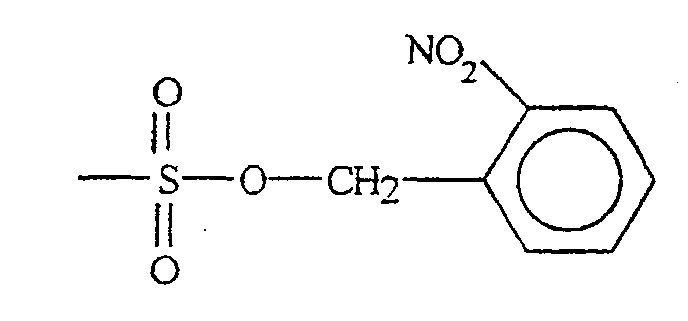
- Precursor acid dopants include (a) o-nitrobenzyl sulfonate side-chains (converting to sulfonic acid group upon irradiation), see figure 3; (b) diazonapthaquinone sulfonate side-chains (converting to indene carboxylic acid upon irradiation), see figure 4; (c) phosphonate or sulfonate ester side-chains, together with an incorporated photoacid generator (PAG) such as one of the onium salts (the onium salts generating a strong protonic acid upon irradiation which cleaves the sulfonate or phosphonate ester leaving group to the corresponding acid), see figure 5.
- PAG photoacid generator
- the conjugated polymer according to the present invention may comprise poly(alkylthiophenes) and poly(alkylfluorenes) or their partners. They should be derivatised with a dopant moiety Y comprising a protonic acid group.
- Suitable protonic acid groups include phosphonic acid, sulfonic acid, carboxylic acid or their precursor in the form of esters, anhydrides, azides, hydrazides, amides, acid chlorides.
- the precursor form is capable of converting to the active protonic acid form under irradiation, thermal exposure, or by reaction with another chemical agent that may be originally deposited with the film or subsequently introduced to the film.
- the acid group or its precursor form could be spaced from the polymer main-chain by an alkyl or aryl spacer and could also be attached as a separate functional unit on the polymer chain.
- a further class of suitable dopant moieties for use in the present method include redox groups based on TCNQ, DDQ, TTF, ferrocene, viologen, iron(III) chelates, or their precursors.
- the precursor form is capable of converting to the active form under irradiation, thermal exposure, or by reaction with another chemical agent.
- These groups could also be spaced from the polymer main chain by an alkyl or aryl spacer or attached to separate functional units on the chain.
- the redox group could accept electrons or donate electrons to the conjugated units, thereby p-doping and n-doping the conjugated units, respectively.
- Partially doped materials formed, for example, as described above could be used to form photonic structures such as distributed Bragg reflectors (potentially pumped reflectors), confinement heterostructures etc.
- photonic structures such as distributed Bragg reflectors (potentially pumped reflectors), confinement heterostructures etc.
- Some examples of device structures which particularly advantageously may include a partially doped conjugated polymer preparable according to the present method are described in our co-pending UK patent application number 9815271.3, the contents of which are incorporated herein by reference.
- the photonic device may include a plurality of layers of such doped materials, the layers alternative in their levels of doping.
- the device could be a mirror, for instance a distributed Bragg reflector.
- Figure 7 shows schematically the energy level structure of a DBR formed by means of partially doped conjugated polymer materials.
- the doping of the materials is controlled so that the HOMO or LUMO levels (depending on whether the mirror is between the anode or the cathode and the emissive layer) of alternate layers of the mirror are at least approximately aligned so that the passage of holes/electrons through the mirror is not significantly impeded at the boundaries between layers of the mirror.
- the thicknesses of the layers of the mirror are chosen to satisfy the conditions for reflection.
- the refractive index of the layers is related to their band gaps, but by means of partial doping the HOMO/LUMO levels can be aligned independently of the band gaps.
- the DBR is formed of conjugated material it could be electrically-pumped to generate photons in addition to reflecting.
- pre-PPV-C1 poly(p-xylylene-alpha-tetrahydrothiophenium chloride)
- pre-PPV-PA poly(p-xylylene-alpha-tetrahydrothiophenium phenylphosphonate) precursor
- the retentate can then be concentrated to the desired concentration and blended with the parent poly(p-xylylene-alpha-tetrahydrothiophenium chloride) in the desired ratio for solution casting. This allows control over the level of doping in the final product.
- Diode structure including partially doped PPV
- diode structures with indium-tin oxide/poly(3,4-dioxy-thiophene):poly(4-styrenesulfonate) composite anodes and calcium cathodes were fabricated for active layers (i) and (ii) defined in Table 1.
- Poly(styrenesulfonic acid-co-styrene) copolymer (PSSH-co-PS) as the “second polymer” is blended in [alkoxylphenyl-PPV]-co-[dialkoxyl-PPV] (P1) or poly(dialkylfluorene-co-triarylamine) (P2) as host. This illustrates the generality of the second aspect of the present invention.
- PSSH-co-PS 0.5 g of polystyrene (4.8 mmol repeat unit) is dissolved with heating into 5 mL anhydrous chloroform in a borosilicate glass reaction flask sealed with teflon-faced silicone rubber septa, and the mixture cooled to -8°C in a bath of calcium chloride and ice-water. 0.01 mL of chlorosulfonic acid (0.15 mmol) is dissolved into 2 mL of chloroform and then syringed into the PS polymer solution. A white cloudy mixture develops almost immediately. The mixture is warmed to room temperature after 30 minutes and 3 mL of water is added, and the mixture optionally refluxed.
- the difference Fourier-transform infrared spectrum of a thin film of the PSSH-co-PS cast on silicon substrates shows the asymmetric and symmetric S-O sulfonate bands at 1000-1200 cm 1 and the appearance of the 2-adjacent hydrogen wagging vibration at 840-860 cm- 1 .
- Increasing the PSSH content to 50 mol% leads to an intractable material that is insoluble in common solvents.
- Increasing the PSSH content further to near 100 mol% gives a material that is soluble in water and methanol.
- the PSSH-co-PS with a low PSSH content less than 10 mol% is therefore compatible with a range of conjugated polymers, and so can be used to regulate the level of doping in these materials.
- a diode structure including a partially doped PPV or polyfluorene
- a substantial reduction in drive voltage for example from 47 V to 9 V at 100 ⁇ A/cm 2 , is achieved upon doping with 10 w/w% of the PSSH-co-PS.
- there is no significant loss of transmission (less than 1% transmission loss) in the sub-gap spectral region of the host polymer. This is because the ratio of PSSH dopant-to-polymer repeat unit is about 0.5 mol%, and the actual doping level (that is, the ratio of ionized PSSH-to-repeat unit) could be even lower depending on the ionization potential of the polymer.
- the difference Fourier-transform infrared spectrum of a thin film of the SP2-co-P2 material cast on silicon substrates shows (i) the asymmetric and symmetric S-O sulfonic bands at 1355 cm -1 and 1175 cm -1 respectively, (ii) the S-O band at 905 cm -1 , (iii) the appearance of the one-hydrogen wagging vibration at 860-880 cm -1 .
- a significant reduction in drive voltage for example from 31 V to 21 V at 100 ⁇ A/cm 2 in 1.1- ⁇ m-thick films, is obtained in the presence of partial doping by an equivalent of 0.05 mol% - 0.1 mol% of sulfonic acid groups. At the same time, there is no significant loss of transmission in the sub-gap spectral region of this P2 polymer.
- This example therefore demonstrates the use of a controlled level of dopant derivatisation of the conjugated polymer to improve the electrical conductivity of conjugated polymer films for use in photonic structures.
- Examples 2 and 3 were repeated but with the sulfonic acid polymer subsequently reacted with quantitative amounts of o-nitrobenzylbromide in chloroform or tetrahydrofuran before film formation to give the o-nitrobenzylsulfonate ester as the precursor dopant.
- the polymer was then blended with the host polymer as in Example 2 or used neat (similar to Example 3) in a suitable solvent and formed into a film.
- the precursor sulfonate ester group was then cleaved by UV exposure to generate the active sulfonic acid group in the film.
- Examples 2 and 3 were repeated but with the sulfonic acid polymer subsequently reacted with excess of methylating agent such as diemthylsulfate before film formation to give the methylsulfonate ester as the precursor dopant.
- the polymer was then blended with small quantities of a photoacid generator such as diphenyliodonium chloride or other diaryliodonium, triarylsulfonium or other onium salts, and further optionally blended with the host polymer (such as in Example 2) or used substantially neat (similar to Example 3) in a suitable solvent and formed into a film.
- the polymer film was then exposed to light or heat to cleave the photoacid generator to produce a strong acid with then cleaves the sulfonate ester to the active sulfonic acid.
- the present invention is not limited to the examples described above.
Landscapes
- Chemical & Material Sciences (AREA)
- Physics & Mathematics (AREA)
- Engineering & Computer Science (AREA)
- Optics & Photonics (AREA)
- Chemical Kinetics & Catalysis (AREA)
- Health & Medical Sciences (AREA)
- Organic Chemistry (AREA)
- Polymers & Plastics (AREA)
- Nanotechnology (AREA)
- Medicinal Chemistry (AREA)
- General Physics & Mathematics (AREA)
- Biophysics (AREA)
- Spectroscopy & Molecular Physics (AREA)
- Microelectronics & Electronic Packaging (AREA)
- Crystallography & Structural Chemistry (AREA)
- Life Sciences & Earth Sciences (AREA)
- Materials Engineering (AREA)
- Manufacturing & Machinery (AREA)
- Compositions Of Macromolecular Compounds (AREA)
- Battery Electrode And Active Subsutance (AREA)
- Polyoxymethylene Polymers And Polymers With Carbon-To-Carbon Bonds (AREA)
- Compounds Of Unknown Constitution (AREA)
- Other Resins Obtained By Reactions Not Involving Carbon-To-Carbon Unsaturated Bonds (AREA)
- Electroluminescent Light Sources (AREA)
- Processes Of Treating Macromolecular Substances (AREA)
Abstract
Description


where n1, n2 are the respective refractive indices; d1, d2 are the corresponding component film thicknesses in the DBR; and λ is the desired reflection wavelength.
| Device structure | Drive voltage required to achieve current density of 1µA/cm2 | Drive voltage required to achieve current density of 10µA/cm2 |
| (i) Undoped 69-nm-thick PPV film with 50 vol% silica | 5.0 V | 7 V |
| (ii) Partially-doped PPV stack having a combined thickness of 207 nm for the films with 50 vol% silica and 171 nm for the neat films, and with an addition 105-nm-thick emitter polymer film | 5.0 V | 10 V |
This illustrates the generality of the second aspect of the present invention.
| Device structure | Drive voltage required to achieve current density of 1µA/cm2 | Drive voltage required to achieve current density of 100µA/cm2 |
| (i) Undoped 1.05-µm-thick P1 film | 5.5 V | 47 V |
| (ii) Partially-doped 1.05-µm-thick P1 film with 1 w/w% of PSSH-co-PS | 2.0 V | 33 V |
| (iii) Partially-doped 1.05-µm-thick P1 film with 10 w/w% of PSSH-co-PS | 1.1 V | 9 V |
| (iv) Undoped 1.65-µm-thick P2 film | 9.5 V | 40 V |
| (v) Partially-doped 1.65-µm-thick P2 film with 1 w/w% of PSSH-co-PS | 5.5 V | 25 V |
| Device structure | Drive voltage for current density of 1µA/cm2 | Drive voltage for current density of 100µA/cm2 |
| (i) Undoped 1.1-µm-thick P2 film | 10.5 V | 31 V |
| (ii) Partially-doped 1.1-µm-thick P2 film with 1 w/w-'s of SP2-co-P2 | 4.5 V | 21 V |
Claims (24)
- A method for partial doping of a host conjugated polymer comprising the step of:blending the host conjugated polymer or a precursor thereof with another substantially-miscible polymer (the "second polymer") which is derivatised with a small fraction of dopant groups or precursors thereof, wherein the small fraction of dopant groups or precursors thereof is selected to be less than the amount required to fully dope the host conjugated polymer.
- A method according to claim 1, wherein the second polymer is a conjugated polymer.
- A method according to claim 1 or claim 2, said method further comprising a step of derivatising with the small fraction of dopant groups or precursors thereof to form the second polymer.
- A method according to any one of the preceding claims, wherein the small fraction is in the range of less than 50% of the amount required to fully dope the host conjugated polymer.
- A method according to any one of the preceding claims, wherein the second polymer is derivatised with precursors of the dopant groups and the method includes heating the precursors to generate the dopant groups.
- A method according to any one of the preceding claims, wherein the method further includes a step of cleaving the dopant groups from the second polymer.
- A method according to any one of the preceding claims, additionally comprising the step of processing to form a film layer comprising the blend.
- A method according to any one of the preceding claims, wherein the host conjugated polymer is selected from the group consisting of alkyl- and alkoxy- derivatives of PPV, poly(fluorenes) and their copolymers.
- A method for partial doping of a host conjugated polymer in solution comprising the step of:incorporating a monomer at a small mole fraction into the host conjugated polymer thereby creating a copolymer, where the monomer is derivatised with a dopant group or its precursor and wherein the small mole fraction of monomers is selected to be less than the amount required to fully dope the host conjugated polymer.
- A method according to claim 9, said method further comprising a step of derivatising the monomers to be incorporated into the host conjugated polymer with the dopant groups or precursors thereof.
- A method according to claim 9 or claim 10, wherein the small fraction is in the range of less than 10-20% of the amount required to fully dope the host conjugated polymer.
- A method according to any one of claims 9 to 11, wherein the monomer is derivatised with a precursor of the dopant group and the method includes heating the precursor to generate the dopant group.
- A method according to any one of claims 9 to 12, wherein the method further includes a step of cleaving the dopant groups from the copolymer.
- A method according to any one of claims 9 to 13, additionally comprising the step of processing to form a film layer comprising the copolymer.
- A method according to any one of claims 9 to 14, wherein the copolymer is selected from the group consisting of alkyl- and alkoxy- derivatives of PPV, poly(fluorenes).
- A method according to any one of the preceding claims, wherein the small fraction is sufficient to form a 0.001% to 5% doped host conjugated polymer.
- A method according to claim 16, wherein the small fraction is sufficient to form a 0.1% to 1% doped host conjugated polymer.
- A method according to any one of the preceding claims, wherein the dopant groups are protonic acid dopant groups.
- A method according to claim 18, wherein the dopant groups or precursors thereof are selected from the group consisting of sulfonic acid, phosphonic acid or their precursors.
- A doped conjugated polymer preparable by the method as defined in any one of the preceding claims.
- A polymer according to claim 20, wherein the dopant groups are distributed substantially homogeneously in the host conjugated polymer matrix.
- A polymer according to claim 20 or claim 21, comprising a light emissive material.
- A photonic device comprising a polymer as defined in any one of claims 20 to 22.
- An optical device comprising a polymer as defined in any one of claims 20 to 22.
Priority Applications (1)
| Application Number | Priority Date | Filing Date | Title |
|---|---|---|---|
| EP08162762A EP1995800B1 (en) | 1999-04-06 | 2000-04-05 | Method for doping a polymer |
Applications Claiming Priority (3)
| Application Number | Priority Date | Filing Date | Title |
|---|---|---|---|
| GBGB9907802.4A GB9907802D0 (en) | 1998-07-14 | 1999-04-06 | Doping |
| GB9907802 | 1999-04-06 | ||
| EP00919019A EP1166281B1 (en) | 1999-04-06 | 2000-04-05 | Method for doping a polymer |
Related Parent Applications (1)
| Application Number | Title | Priority Date | Filing Date |
|---|---|---|---|
| EP00919019A Division EP1166281B1 (en) | 1999-04-06 | 2000-04-05 | Method for doping a polymer |
Related Child Applications (1)
| Application Number | Title | Priority Date | Filing Date |
|---|---|---|---|
| EP08162762A Division EP1995800B1 (en) | 1999-04-06 | 2000-04-05 | Method for doping a polymer |
Publications (3)
| Publication Number | Publication Date |
|---|---|
| EP1432051A2 true EP1432051A2 (en) | 2004-06-23 |
| EP1432051A3 EP1432051A3 (en) | 2007-11-07 |
| EP1432051B1 EP1432051B1 (en) | 2008-10-08 |
Family
ID=10850999
Family Applications (3)
| Application Number | Title | Priority Date | Filing Date |
|---|---|---|---|
| EP04075962A Expired - Lifetime EP1432051B1 (en) | 1999-04-06 | 2000-04-05 | Method for doping a polymer |
| EP00919019A Expired - Lifetime EP1166281B1 (en) | 1999-04-06 | 2000-04-05 | Method for doping a polymer |
| EP08162762A Expired - Lifetime EP1995800B1 (en) | 1999-04-06 | 2000-04-05 | Method for doping a polymer |
Family Applications After (2)
| Application Number | Title | Priority Date | Filing Date |
|---|---|---|---|
| EP00919019A Expired - Lifetime EP1166281B1 (en) | 1999-04-06 | 2000-04-05 | Method for doping a polymer |
| EP08162762A Expired - Lifetime EP1995800B1 (en) | 1999-04-06 | 2000-04-05 | Method for doping a polymer |
Country Status (10)
| Country | Link |
|---|---|
| US (4) | US6835803B1 (en) |
| EP (3) | EP1432051B1 (en) |
| JP (2) | JP4486758B2 (en) |
| KR (2) | KR100674686B1 (en) |
| CN (2) | CN101319045B (en) |
| AT (3) | ATE410791T1 (en) |
| AU (1) | AU3977900A (en) |
| DE (3) | DE60012000T2 (en) |
| HK (1) | HK1046771B (en) |
| WO (1) | WO2000060612A1 (en) |
Cited By (1)
| Publication number | Priority date | Publication date | Assignee | Title |
|---|---|---|---|---|
| US9650245B2 (en) | 2002-08-09 | 2017-05-16 | Semiconductor Energy Laboratory Co., Ltd. | Organic electroluminescent device |
Families Citing this family (34)
| Publication number | Priority date | Publication date | Assignee | Title |
|---|---|---|---|---|
| ATE410791T1 (en) * | 1999-04-06 | 2008-10-15 | Cambridge Display Tech Ltd | METHOD FOR DOPPING POLYMERS |
| WO2000076008A1 (en) | 1999-06-09 | 2000-12-14 | Cambridge Display Technology Limited | Method of producing organic light-emissive devices |
| EP1289342B1 (en) * | 2001-09-04 | 2006-11-22 | Sony Deutschland GmbH | Aligned emissive polymer blends, film and device based thereon |
| SG111090A1 (en) * | 2002-10-25 | 2005-05-30 | Agency Science Tech & Res | Cationic water-soluble conjugated polymers and their precursors |
| JP2004343051A (en) * | 2003-01-25 | 2004-12-02 | Merck Patent Gmbh | Polymer dopant |
| EP1441399A3 (en) * | 2003-01-25 | 2009-07-01 | MERCK PATENT GmbH | Polymer dopants |
| DE102004007399B4 (en) * | 2004-02-16 | 2007-12-27 | Fraunhofer-Gesellschaft zur Förderung der angewandten Forschung e.V. | Polymer system with defined adjustable carrier mobility and its use |
| EP2918590A1 (en) * | 2004-03-11 | 2015-09-16 | Mitsubishi Chemical Corporation | Composition for charge-transport film and ionic compound, charge-transport film and organic electroluminescence device using the same, and production method of the organic electroluminescence device and production method of the charge-transport film |
| US6930322B1 (en) * | 2004-03-26 | 2005-08-16 | Matsushita Electric Industrial Co., Ltd. | Combination insulator and organic semiconductor formed from self-assembling block co-polymers |
| US7795617B2 (en) * | 2004-10-29 | 2010-09-14 | Semiconductor Energy Laboratory Co., Ltd. | Semiconductor device, IC card, IC tag, RFID, transponder, paper money, valuable securities, passport, electronic device, bag, and clothes |
| KR100715548B1 (en) * | 2005-07-29 | 2007-05-07 | 광 석 서 | Conductive Polymers Synthesized Using Partially Substituted Polymer Dopants |
| KR20080043772A (en) * | 2005-08-01 | 2008-05-19 | 플렉스트로닉스, 인크 | Potential Doping of Conductive Polymers |
| WO2007018039A1 (en) * | 2005-08-05 | 2007-02-15 | Matsushita Electric Industrial Co., Ltd. | Semiconductor light-emitting device |
| US20070077452A1 (en) * | 2005-10-04 | 2007-04-05 | Jie Liu | Organic light emitting devices having latent activated layers and methods of fabricating the same |
| US20070176167A1 (en) * | 2006-01-27 | 2007-08-02 | General Electric Company | Method of making organic light emitting devices |
| JP5683104B2 (en) * | 2006-03-21 | 2015-03-11 | ノヴァレッド・アクチエンゲゼルシャフト | Process for the production of doped organic semiconductor materials and formulations used therefor |
| GB0617723D0 (en) * | 2006-09-08 | 2006-10-18 | Cambridge Display Tech Ltd | Conductive polymer compositions in opto-electrical devices |
| EP1912268B1 (en) * | 2006-10-09 | 2020-01-01 | Novaled GmbH | Method for spatial structuring the emission density of an OLED, semiconductor device obtained by the method and its use |
| US20080145697A1 (en) * | 2006-12-13 | 2008-06-19 | General Electric Company | Opto-electronic devices containing sulfonated light-emitting copolymers |
| DE102008046857B4 (en) | 2007-12-17 | 2025-03-27 | Pictiva Displays International Limited | OLED for AC operation and manufacturing processes |
| KR101683026B1 (en) * | 2008-04-11 | 2016-12-07 | 닛산 가가쿠 고교 가부시키 가이샤 | Doped conjugated polymers, devices, and methods of making devices |
| EP2291872A1 (en) * | 2008-06-27 | 2011-03-09 | Universal Display Corporation | Cross linkable ionic dopants |
| JP2010212212A (en) * | 2009-03-12 | 2010-09-24 | Sanyo Electric Co Ltd | Conductive polymer film, conductive polymer material, and electronic device |
| WO2012121417A1 (en) * | 2011-03-09 | 2012-09-13 | Waseda University | Conducting polymer / redox polymer blends via in-situ oxidative polymerization - preparation methods and application as an electro-active polymeric materials |
| KR101936978B1 (en) * | 2011-07-05 | 2019-01-09 | 닛산 가가쿠 가부시키가이샤 | Vertically phase-separating semiconducting organic material layers |
| EA028833B1 (en) | 2014-09-30 | 2018-01-31 | Сикпа Холдинг Са | Liquid containing polymer marker, use of a polymer marker as authentication tool, and method and device for detecting a polymer marker dissolved in a liquid |
| WO2016126209A1 (en) * | 2015-02-03 | 2016-08-11 | National University Of Singapore | P-doped electrically conductive polymeric materials for hole-injection and hole-extraction layers |
| GB2544768A (en) * | 2015-11-25 | 2017-05-31 | Cambridge Display Tech Ltd | Charge transfer salt, electronic device and method of forming the same |
| US11005042B2 (en) * | 2015-12-10 | 2021-05-11 | Merck Patent Gmbh | Formulations containing ketones comprising non-aromatic cycles |
| WO2017136598A1 (en) * | 2016-02-02 | 2017-08-10 | Polydrop, Llc | Transparent conjugated polymer films |
| GB2551730A (en) | 2016-06-28 | 2018-01-03 | Sumitomo Chemical Co | Method and composition |
| US20180240565A1 (en) | 2017-02-17 | 2018-08-23 | Polydrop, Llc | Conductive polymer-matrix compositions and uses thereof |
| NL2022110B1 (en) | 2018-11-30 | 2020-06-26 | Univ Delft Tech | Electrochemical doping of semiconductor materials |
| JP2021144973A (en) * | 2020-03-10 | 2021-09-24 | 三菱ケミカル株式会社 | Photoelectric conversion element and electric power generation device |
Family Cites Families (22)
| Publication number | Priority date | Publication date | Assignee | Title |
|---|---|---|---|---|
| US422903A (en) * | 1890-03-11 | Anti-friction journal | ||
| JPS5279255A (en) | 1975-12-25 | 1977-07-04 | Nippon Electric Co | Solid state electrolytic capacitor |
| US4222903A (en) * | 1978-05-04 | 1980-09-16 | University Patents, Inc. | P-Type electrically conducting doped polyacetylene film and method of preparing same |
| JPS5817609A (en) * | 1981-07-24 | 1983-02-01 | 三洋電機株式会社 | Solid electrolytic condenser and method of pruducing same |
| JPS58123715A (en) * | 1982-01-18 | 1983-07-23 | 三洋電機株式会社 | Solid electrolytic condenser |
| JPS6037114A (en) * | 1983-08-09 | 1985-02-26 | 昭和電工株式会社 | Solid electrolytic condenser |
| JPS6147625A (en) * | 1984-08-14 | 1986-03-08 | 昭和電工株式会社 | Solid electrolytic condenser |
| WO1987005914A1 (en) * | 1986-03-24 | 1987-10-08 | The Regents Of The University Of California | Self-doped polymers |
| DE3736114A1 (en) * | 1987-10-26 | 1989-07-13 | Hoechst Ag | MODIFIED ELECTRICALLY CONDUCTING POLYMERS |
| JP2813428B2 (en) * | 1989-08-17 | 1998-10-22 | 三菱電機株式会社 | Field effect transistor and liquid crystal display device using the field effect transistor |
| JPH04222903A (en) * | 1990-12-25 | 1992-08-12 | Olympus Optical Co Ltd | Magneto-optical driving device |
| US5378404A (en) * | 1991-04-22 | 1995-01-03 | Alliedsignal Inc. | Process for forming dispersions or solutions of electrically conductive conjugated polymers in a polymeric or liquid phase |
| CA2111150C (en) | 1991-06-12 | 2001-10-30 | Yong Cao | Processible forms of electrically conductive polyaniline and conductive products formed therefrom |
| JPH07192790A (en) | 1993-12-27 | 1995-07-28 | Showa Denko Kk | Anisotropic conductive connection material |
| JP3235475B2 (en) * | 1996-07-16 | 2001-12-04 | 日本電気株式会社 | Solid electrolytic capacitor and method of manufacturing the same |
| JP3861131B2 (en) | 1997-05-16 | 2006-12-20 | 独立行政法人産業技術総合研究所 | Organic nonlinear optical materials |
| GB9713074D0 (en) * | 1997-06-21 | 1997-08-27 | Cambridge Display Tech Ltd | Electrically-conducting colour filters for use in organic light-emitting displays |
| WO1999060586A1 (en) * | 1998-05-21 | 1999-11-25 | Showa Denko K.K. | Solid electrolytic capacitor and method for preparing the same |
| GB9815271D0 (en) * | 1998-07-14 | 1998-09-09 | Cambridge Display Tech Ltd | Particles and devices comprising particles |
| ATE410791T1 (en) * | 1999-04-06 | 2008-10-15 | Cambridge Display Tech Ltd | METHOD FOR DOPPING POLYMERS |
| GB0004593D0 (en) | 2000-02-25 | 2000-04-19 | Springbar Water Coolers Limite | Water bottle |
| JP5279255B2 (en) | 2007-12-20 | 2013-09-04 | 花王株式会社 | Ink set for inkjet recording |
-
2000
- 2000-04-05 AT AT04075962T patent/ATE410791T1/en not_active IP Right Cessation
- 2000-04-05 KR KR1020017012766A patent/KR100674686B1/en not_active Expired - Fee Related
- 2000-04-05 HK HK02108243.6A patent/HK1046771B/en not_active IP Right Cessation
- 2000-04-05 KR KR1020067019695A patent/KR100667290B1/en not_active Expired - Fee Related
- 2000-04-05 US US09/958,257 patent/US6835803B1/en not_active Expired - Lifetime
- 2000-04-05 EP EP04075962A patent/EP1432051B1/en not_active Expired - Lifetime
- 2000-04-05 EP EP00919019A patent/EP1166281B1/en not_active Expired - Lifetime
- 2000-04-05 WO PCT/GB2000/001288 patent/WO2000060612A1/en not_active Ceased
- 2000-04-05 EP EP08162762A patent/EP1995800B1/en not_active Expired - Lifetime
- 2000-04-05 JP JP2000610019A patent/JP4486758B2/en not_active Expired - Lifetime
- 2000-04-05 AU AU39779/00A patent/AU3977900A/en not_active Abandoned
- 2000-04-05 CN CN2008101356573A patent/CN101319045B/en not_active Expired - Lifetime
- 2000-04-05 AT AT00919019T patent/ATE270788T1/en not_active IP Right Cessation
- 2000-04-05 DE DE60012000T patent/DE60012000T2/en not_active Expired - Lifetime
- 2000-04-05 CN CNB008070512A patent/CN100412994C/en not_active Expired - Lifetime
- 2000-04-05 DE DE60040492T patent/DE60040492D1/en not_active Expired - Lifetime
- 2000-04-05 AT AT08162762T patent/ATE470958T1/en not_active IP Right Cessation
- 2000-04-05 DE DE60044543T patent/DE60044543D1/en not_active Expired - Lifetime
-
2004
- 2004-04-07 US US10/819,622 patent/US7008999B2/en not_active Expired - Lifetime
-
2006
- 2006-03-03 US US11/367,127 patent/US7279524B2/en not_active Expired - Lifetime
-
2007
- 2007-10-09 US US11/869,662 patent/US8748534B2/en not_active Expired - Fee Related
- 2007-12-17 JP JP2007324548A patent/JP2008156636A/en active Pending
Cited By (1)
| Publication number | Priority date | Publication date | Assignee | Title |
|---|---|---|---|---|
| US9650245B2 (en) | 2002-08-09 | 2017-05-16 | Semiconductor Energy Laboratory Co., Ltd. | Organic electroluminescent device |
Also Published As
Similar Documents
| Publication | Publication Date | Title |
|---|---|---|
| EP1166281B1 (en) | Method for doping a polymer | |
| KR100714386B1 (en) | Optoelectronic devices | |
| KR101942025B1 (en) | Films containing electrically conductive polymers | |
| EP0544771B1 (en) | Patterning of semiconductive polymers | |
| KR101162934B1 (en) | Electronic devices comprising organic semiconductors | |
| Yi et al. | Molecular design of diazo compound for carbene-mediated cross-linking of hole-transport polymer in QLED with reduced energy barrier and improved charge balance | |
| Bae et al. | Reduced efficiency roll-off in light-emitting diodes enabled by quantum dot–conducting polymer nanohybrids | |
| Winkler et al. | Novel poly (p-phenylene vinylene) derivatives with oligo (ethylene oxide) side chains: synthesis and pattern formation | |
| JP6551597B2 (en) | Non-aqueous ink composition containing metal nanoparticles suitable for use in organic electronic devices | |
| US8308987B2 (en) | Conductive polymer compositions in opto-electrical devices | |
| KR20190102077A (en) | Ink Compositions Containing Sulfonated Conjugated Polymers |
Legal Events
| Date | Code | Title | Description |
|---|---|---|---|
| PUAI | Public reference made under article 153(3) epc to a published international application that has entered the european phase |
Free format text: ORIGINAL CODE: 0009012 |
|
| AC | Divisional application: reference to earlier application |
Ref document number: 1166281 Country of ref document: EP Kind code of ref document: P |
|
| AK | Designated contracting states |
Kind code of ref document: A2 Designated state(s): AT BE CH CY DE DK ES FI FR GB GR IE IT LI LU MC NL PT SE |
|
| RIN1 | Information on inventor provided before grant (corrected) |
Inventor name: KIM, JI-SEON Inventor name: HO, PETER KIAN-HOON,DMSFS - N. UNIV. SINGAPORE Inventor name: FRIEND, RICHARD HENRY |
|
| 111Z | Information provided on other rights and legal means of execution |
Free format text: ATBECHCYDEDKESFIFRGBGRIEITLILUMCNLPTSE Effective date: 20040930 |
|
| PUAL | Search report despatched |
Free format text: ORIGINAL CODE: 0009013 |
|
| AK | Designated contracting states |
Kind code of ref document: A3 Designated state(s): AT BE CH CY DE DK ES FI FR GB GR IE IT LI LU MC NL PT SE |
|
| RIC1 | Information provided on ipc code assigned before grant |
Ipc: H01L 51/00 20060101AFI20071004BHEP |
|
| 17P | Request for examination filed |
Effective date: 20080314 |
|
| GRAP | Despatch of communication of intention to grant a patent |
Free format text: ORIGINAL CODE: EPIDOSNIGR1 |
|
| AKX | Designation fees paid |
Designated state(s): AT BE CH CY DE DK ES FI FR GB GR IE IT LI LU MC NL PT SE |
|
| GRAS | Grant fee paid |
Free format text: ORIGINAL CODE: EPIDOSNIGR3 |
|
| GRAA | (expected) grant |
Free format text: ORIGINAL CODE: 0009210 |
|
| AC | Divisional application: reference to earlier application |
Ref document number: 1166281 Country of ref document: EP Kind code of ref document: P |
|
| AK | Designated contracting states |
Kind code of ref document: B1 Designated state(s): AT BE CH CY DE DK ES FI FR GB GR IE IT LI LU MC NL PT SE |
|
| REG | Reference to a national code |
Ref country code: GB Ref legal event code: FG4D |
|
| REG | Reference to a national code |
Ref country code: CH Ref legal event code: EP |
|
| REG | Reference to a national code |
Ref country code: IE Ref legal event code: FG4D |
|
| REF | Corresponds to: |
Ref document number: 60040492 Country of ref document: DE Date of ref document: 20081120 Kind code of ref document: P |
|
| NLV1 | Nl: lapsed or annulled due to failure to fulfill the requirements of art. 29p and 29m of the patents act | ||
| PG25 | Lapsed in a contracting state [announced via postgrant information from national office to epo] |
Ref country code: AT Free format text: LAPSE BECAUSE OF FAILURE TO SUBMIT A TRANSLATION OF THE DESCRIPTION OR TO PAY THE FEE WITHIN THE PRESCRIBED TIME-LIMIT Effective date: 20081008 Ref country code: ES Free format text: LAPSE BECAUSE OF FAILURE TO SUBMIT A TRANSLATION OF THE DESCRIPTION OR TO PAY THE FEE WITHIN THE PRESCRIBED TIME-LIMIT Effective date: 20090119 |
|
| PG25 | Lapsed in a contracting state [announced via postgrant information from national office to epo] |
Ref country code: PT Free format text: LAPSE BECAUSE OF FAILURE TO SUBMIT A TRANSLATION OF THE DESCRIPTION OR TO PAY THE FEE WITHIN THE PRESCRIBED TIME-LIMIT Effective date: 20090218 Ref country code: FI Free format text: LAPSE BECAUSE OF FAILURE TO SUBMIT A TRANSLATION OF THE DESCRIPTION OR TO PAY THE FEE WITHIN THE PRESCRIBED TIME-LIMIT Effective date: 20081008 Ref country code: NL Free format text: LAPSE BECAUSE OF FAILURE TO SUBMIT A TRANSLATION OF THE DESCRIPTION OR TO PAY THE FEE WITHIN THE PRESCRIBED TIME-LIMIT Effective date: 20081008 |
|
| PG25 | Lapsed in a contracting state [announced via postgrant information from national office to epo] |
Ref country code: DK Free format text: LAPSE BECAUSE OF FAILURE TO SUBMIT A TRANSLATION OF THE DESCRIPTION OR TO PAY THE FEE WITHIN THE PRESCRIBED TIME-LIMIT Effective date: 20081008 Ref country code: BE Free format text: LAPSE BECAUSE OF FAILURE TO SUBMIT A TRANSLATION OF THE DESCRIPTION OR TO PAY THE FEE WITHIN THE PRESCRIBED TIME-LIMIT Effective date: 20081008 |
|
| PLBE | No opposition filed within time limit |
Free format text: ORIGINAL CODE: 0009261 |
|
| STAA | Information on the status of an ep patent application or granted ep patent |
Free format text: STATUS: NO OPPOSITION FILED WITHIN TIME LIMIT |
|
| PG25 | Lapsed in a contracting state [announced via postgrant information from national office to epo] |
Ref country code: SE Free format text: LAPSE BECAUSE OF FAILURE TO SUBMIT A TRANSLATION OF THE DESCRIPTION OR TO PAY THE FEE WITHIN THE PRESCRIBED TIME-LIMIT Effective date: 20090108 Ref country code: IT Free format text: LAPSE BECAUSE OF FAILURE TO SUBMIT A TRANSLATION OF THE DESCRIPTION OR TO PAY THE FEE WITHIN THE PRESCRIBED TIME-LIMIT Effective date: 20081008 |
|
| 26N | No opposition filed |
Effective date: 20090709 |
|
| REG | Reference to a national code |
Ref country code: CH Ref legal event code: PL |
|
| REG | Reference to a national code |
Ref country code: FR Ref legal event code: ST Effective date: 20091231 |
|
| PG25 | Lapsed in a contracting state [announced via postgrant information from national office to epo] |
Ref country code: LI Free format text: LAPSE BECAUSE OF NON-PAYMENT OF DUE FEES Effective date: 20090430 Ref country code: CH Free format text: LAPSE BECAUSE OF NON-PAYMENT OF DUE FEES Effective date: 20090430 |
|
| PG25 | Lapsed in a contracting state [announced via postgrant information from national office to epo] |
Ref country code: MC Free format text: LAPSE BECAUSE OF NON-PAYMENT OF DUE FEES Effective date: 20090430 Ref country code: FR Free format text: LAPSE BECAUSE OF NON-PAYMENT OF DUE FEES Effective date: 20091222 Ref country code: IE Free format text: LAPSE BECAUSE OF NON-PAYMENT OF DUE FEES Effective date: 20090405 |
|
| PG25 | Lapsed in a contracting state [announced via postgrant information from national office to epo] |
Ref country code: GR Free format text: LAPSE BECAUSE OF FAILURE TO SUBMIT A TRANSLATION OF THE DESCRIPTION OR TO PAY THE FEE WITHIN THE PRESCRIBED TIME-LIMIT Effective date: 20090109 |
|
| PG25 | Lapsed in a contracting state [announced via postgrant information from national office to epo] |
Ref country code: LU Free format text: LAPSE BECAUSE OF NON-PAYMENT OF DUE FEES Effective date: 20090405 |
|
| PG25 | Lapsed in a contracting state [announced via postgrant information from national office to epo] |
Ref country code: CY Free format text: LAPSE BECAUSE OF FAILURE TO SUBMIT A TRANSLATION OF THE DESCRIPTION OR TO PAY THE FEE WITHIN THE PRESCRIBED TIME-LIMIT Effective date: 20081008 |
|
| PGFP | Annual fee paid to national office [announced via postgrant information from national office to epo] |
Ref country code: GB Payment date: 20190326 Year of fee payment: 20 |
|
| PGFP | Annual fee paid to national office [announced via postgrant information from national office to epo] |
Ref country code: DE Payment date: 20190318 Year of fee payment: 20 |
|
| REG | Reference to a national code |
Ref country code: DE Ref legal event code: R071 Ref document number: 60040492 Country of ref document: DE |
|
| REG | Reference to a national code |
Ref country code: GB Ref legal event code: PE20 Expiry date: 20200404 |
|
| PG25 | Lapsed in a contracting state [announced via postgrant information from national office to epo] |
Ref country code: GB Free format text: LAPSE BECAUSE OF EXPIRATION OF PROTECTION Effective date: 20200404 |