EP1432028A1 - Production method for semiconductor device - Google Patents
Production method for semiconductor device Download PDFInfo
- Publication number
- EP1432028A1 EP1432028A1 EP02799472A EP02799472A EP1432028A1 EP 1432028 A1 EP1432028 A1 EP 1432028A1 EP 02799472 A EP02799472 A EP 02799472A EP 02799472 A EP02799472 A EP 02799472A EP 1432028 A1 EP1432028 A1 EP 1432028A1
- Authority
- EP
- European Patent Office
- Prior art keywords
- substrate
- film
- semiconductor device
- manufacturing
- silica derivative
- Prior art date
- Legal status (The legal status is an assumption and is not a legal conclusion. Google has not performed a legal analysis and makes no representation as to the accuracy of the status listed.)
- Withdrawn
Links
Images


Classifications
-
- H—ELECTRICITY
- H10—SEMICONDUCTOR DEVICES; ELECTRIC SOLID-STATE DEVICES NOT OTHERWISE PROVIDED FOR
- H10P—GENERIC PROCESSES OR APPARATUS FOR THE MANUFACTURE OR TREATMENT OF DEVICES COVERED BY CLASS H10
- H10P14/00—Formation of materials, e.g. in the shape of layers or pillars
- H10P14/60—Formation of materials, e.g. in the shape of layers or pillars of insulating materials
- H10P14/69—Inorganic materials
- H10P14/692—Inorganic materials composed of oxides, glassy oxides or oxide-based glasses
- H10P14/6938—Inorganic materials composed of oxides, glassy oxides or oxide-based glasses the material containing at least one metal element, e.g. metal oxides, metal oxynitrides or metal oxycarbides
- H10P14/69398—Inorganic materials composed of oxides, glassy oxides or oxide-based glasses the material containing at least one metal element, e.g. metal oxides, metal oxynitrides or metal oxycarbides the material having a perovskite structure, e.g. BaTiO3
-
- H—ELECTRICITY
- H10—SEMICONDUCTOR DEVICES; ELECTRIC SOLID-STATE DEVICES NOT OTHERWISE PROVIDED FOR
- H10P—GENERIC PROCESSES OR APPARATUS FOR THE MANUFACTURE OR TREATMENT OF DEVICES COVERED BY CLASS H10
- H10P14/00—Formation of materials, e.g. in the shape of layers or pillars
- H10P14/60—Formation of materials, e.g. in the shape of layers or pillars of insulating materials
-
- H—ELECTRICITY
- H10—SEMICONDUCTOR DEVICES; ELECTRIC SOLID-STATE DEVICES NOT OTHERWISE PROVIDED FOR
- H10B—ELECTRONIC MEMORY DEVICES
- H10B53/00—Ferroelectric RAM [FeRAM] devices comprising ferroelectric memory capacitors
-
- H—ELECTRICITY
- H10—SEMICONDUCTOR DEVICES; ELECTRIC SOLID-STATE DEVICES NOT OTHERWISE PROVIDED FOR
- H10B—ELECTRONIC MEMORY DEVICES
- H10B53/00—Ferroelectric RAM [FeRAM] devices comprising ferroelectric memory capacitors
- H10B53/30—Ferroelectric RAM [FeRAM] devices comprising ferroelectric memory capacitors characterised by the memory core region
-
- H—ELECTRICITY
- H10—SEMICONDUCTOR DEVICES; ELECTRIC SOLID-STATE DEVICES NOT OTHERWISE PROVIDED FOR
- H10P—GENERIC PROCESSES OR APPARATUS FOR THE MANUFACTURE OR TREATMENT OF DEVICES COVERED BY CLASS H10
- H10P14/00—Formation of materials, e.g. in the shape of layers or pillars
- H10P14/60—Formation of materials, e.g. in the shape of layers or pillars of insulating materials
- H10P14/65—Formation of materials, e.g. in the shape of layers or pillars of insulating materials characterised by treatments performed before or after the formation of the materials
- H10P14/6516—Formation of materials, e.g. in the shape of layers or pillars of insulating materials characterised by treatments performed before or after the formation of the materials of treatments performed after formation of the materials
- H10P14/6529—Formation of materials, e.g. in the shape of layers or pillars of insulating materials characterised by treatments performed before or after the formation of the materials of treatments performed after formation of the materials by exposure to a gas or vapour
-
- H—ELECTRICITY
- H10—SEMICONDUCTOR DEVICES; ELECTRIC SOLID-STATE DEVICES NOT OTHERWISE PROVIDED FOR
- H10W—GENERIC PACKAGES, INTERCONNECTIONS, CONNECTORS OR OTHER CONSTRUCTIONAL DETAILS OF DEVICES COVERED BY CLASS H10
- H10W20/00—Interconnections in chips, wafers or substrates
- H10W20/01—Manufacture or treatment
- H10W20/071—Manufacture or treatment of dielectric parts thereof
- H10W20/072—Manufacture or treatment of dielectric parts thereof of dielectric parts comprising air gaps
-
- H—ELECTRICITY
- H10—SEMICONDUCTOR DEVICES; ELECTRIC SOLID-STATE DEVICES NOT OTHERWISE PROVIDED FOR
- H10W—GENERIC PACKAGES, INTERCONNECTIONS, CONNECTORS OR OTHER CONSTRUCTIONAL DETAILS OF DEVICES COVERED BY CLASS H10
- H10W20/00—Interconnections in chips, wafers or substrates
- H10W20/40—Interconnections external to wafers or substrates, e.g. back-end-of-line [BEOL] metallisations or vias connecting to gate electrodes
- H10W20/45—Interconnections external to wafers or substrates, e.g. back-end-of-line [BEOL] metallisations or vias connecting to gate electrodes characterised by their insulating parts
- H10W20/46—Interconnections external to wafers or substrates, e.g. back-end-of-line [BEOL] metallisations or vias connecting to gate electrodes characterised by their insulating parts comprising air gaps
-
- H—ELECTRICITY
- H10—SEMICONDUCTOR DEVICES; ELECTRIC SOLID-STATE DEVICES NOT OTHERWISE PROVIDED FOR
- H10W—GENERIC PACKAGES, INTERCONNECTIONS, CONNECTORS OR OTHER CONSTRUCTIONAL DETAILS OF DEVICES COVERED BY CLASS H10
- H10W20/00—Interconnections in chips, wafers or substrates
- H10W20/40—Interconnections external to wafers or substrates, e.g. back-end-of-line [BEOL] metallisations or vias connecting to gate electrodes
- H10W20/45—Interconnections external to wafers or substrates, e.g. back-end-of-line [BEOL] metallisations or vias connecting to gate electrodes characterised by their insulating parts
- H10W20/48—Insulating materials thereof
-
- H—ELECTRICITY
- H10—SEMICONDUCTOR DEVICES; ELECTRIC SOLID-STATE DEVICES NOT OTHERWISE PROVIDED FOR
- H10W—GENERIC PACKAGES, INTERCONNECTIONS, CONNECTORS OR OTHER CONSTRUCTIONAL DETAILS OF DEVICES COVERED BY CLASS H10
- H10W20/00—Interconnections in chips, wafers or substrates
- H10W20/40—Interconnections external to wafers or substrates, e.g. back-end-of-line [BEOL] metallisations or vias connecting to gate electrodes
- H10W20/495—Capacitive arrangements or effects of, or between wiring layers
-
- H—ELECTRICITY
- H10—SEMICONDUCTOR DEVICES; ELECTRIC SOLID-STATE DEVICES NOT OTHERWISE PROVIDED FOR
- H10W—GENERIC PACKAGES, INTERCONNECTIONS, CONNECTORS OR OTHER CONSTRUCTIONAL DETAILS OF DEVICES COVERED BY CLASS H10
- H10W74/00—Encapsulations, e.g. protective coatings
- H10W74/10—Encapsulations, e.g. protective coatings characterised by their shape or disposition
- H10W74/131—Encapsulations, e.g. protective coatings characterised by their shape or disposition the semiconductor body being only partially enclosed
- H10W74/137—Encapsulations, e.g. protective coatings characterised by their shape or disposition the semiconductor body being only partially enclosed the encapsulations being directly on the semiconductor body
-
- H—ELECTRICITY
- H10—SEMICONDUCTOR DEVICES; ELECTRIC SOLID-STATE DEVICES NOT OTHERWISE PROVIDED FOR
- H10P—GENERIC PROCESSES OR APPARATUS FOR THE MANUFACTURE OR TREATMENT OF DEVICES COVERED BY CLASS H10
- H10P14/00—Formation of materials, e.g. in the shape of layers or pillars
- H10P14/60—Formation of materials, e.g. in the shape of layers or pillars of insulating materials
- H10P14/63—Formation of materials, e.g. in the shape of layers or pillars of insulating materials characterised by the formation processes
- H10P14/6326—Deposition processes
- H10P14/6342—Liquid deposition, e.g. spin-coating, sol-gel techniques or spray coating
-
- H—ELECTRICITY
- H10—SEMICONDUCTOR DEVICES; ELECTRIC SOLID-STATE DEVICES NOT OTHERWISE PROVIDED FOR
- H10P—GENERIC PROCESSES OR APPARATUS FOR THE MANUFACTURE OR TREATMENT OF DEVICES COVERED BY CLASS H10
- H10P14/00—Formation of materials, e.g. in the shape of layers or pillars
- H10P14/60—Formation of materials, e.g. in the shape of layers or pillars of insulating materials
- H10P14/66—Formation of materials, e.g. in the shape of layers or pillars of insulating materials characterised by the type of materials
- H10P14/665—Porous materials
-
- H—ELECTRICITY
- H10—SEMICONDUCTOR DEVICES; ELECTRIC SOLID-STATE DEVICES NOT OTHERWISE PROVIDED FOR
- H10P—GENERIC PROCESSES OR APPARATUS FOR THE MANUFACTURE OR TREATMENT OF DEVICES COVERED BY CLASS H10
- H10P14/00—Formation of materials, e.g. in the shape of layers or pillars
- H10P14/60—Formation of materials, e.g. in the shape of layers or pillars of insulating materials
- H10P14/66—Formation of materials, e.g. in the shape of layers or pillars of insulating materials characterised by the type of materials
- H10P14/668—Formation of materials, e.g. in the shape of layers or pillars of insulating materials characterised by the type of materials the materials being characterised by the deposition precursor materials
- H10P14/6681—Formation of materials, e.g. in the shape of layers or pillars of insulating materials characterised by the type of materials the materials being characterised by the deposition precursor materials the precursor containing a compound comprising Si
- H10P14/6684—Formation of materials, e.g. in the shape of layers or pillars of insulating materials characterised by the type of materials the materials being characterised by the deposition precursor materials the precursor containing a compound comprising Si the compound comprising silicon and oxygen
- H10P14/6686—Formation of materials, e.g. in the shape of layers or pillars of insulating materials characterised by the type of materials the materials being characterised by the deposition precursor materials the precursor containing a compound comprising Si the compound comprising silicon and oxygen the compound being a molecule comprising at least one silicon-oxygen bond and the compound having hydrogen or an organic group attached to the silicon or oxygen, e.g. a siloxane
-
- H—ELECTRICITY
- H10—SEMICONDUCTOR DEVICES; ELECTRIC SOLID-STATE DEVICES NOT OTHERWISE PROVIDED FOR
- H10P—GENERIC PROCESSES OR APPARATUS FOR THE MANUFACTURE OR TREATMENT OF DEVICES COVERED BY CLASS H10
- H10P14/00—Formation of materials, e.g. in the shape of layers or pillars
- H10P14/60—Formation of materials, e.g. in the shape of layers or pillars of insulating materials
- H10P14/69—Inorganic materials
- H10P14/692—Inorganic materials composed of oxides, glassy oxides or oxide-based glasses
- H10P14/6921—Inorganic materials composed of oxides, glassy oxides or oxide-based glasses containing silicon
- H10P14/69215—Inorganic materials composed of oxides, glassy oxides or oxide-based glasses containing silicon the material being a silicon oxide, e.g. SiO2
-
- H—ELECTRICITY
- H10—SEMICONDUCTOR DEVICES; ELECTRIC SOLID-STATE DEVICES NOT OTHERWISE PROVIDED FOR
- H10P—GENERIC PROCESSES OR APPARATUS FOR THE MANUFACTURE OR TREATMENT OF DEVICES COVERED BY CLASS H10
- H10P14/00—Formation of materials, e.g. in the shape of layers or pillars
- H10P14/60—Formation of materials, e.g. in the shape of layers or pillars of insulating materials
- H10P14/69—Inorganic materials
- H10P14/692—Inorganic materials composed of oxides, glassy oxides or oxide-based glasses
- H10P14/6921—Inorganic materials composed of oxides, glassy oxides or oxide-based glasses containing silicon
- H10P14/6922—Inorganic materials composed of oxides, glassy oxides or oxide-based glasses containing silicon the material containing Si, O and at least one of H, N, C, F or other non-metal elements, e.g. SiOC, SiOC:H or SiONC
-
- H—ELECTRICITY
- H10—SEMICONDUCTOR DEVICES; ELECTRIC SOLID-STATE DEVICES NOT OTHERWISE PROVIDED FOR
- H10W—GENERIC PACKAGES, INTERCONNECTIONS, CONNECTORS OR OTHER CONSTRUCTIONAL DETAILS OF DEVICES COVERED BY CLASS H10
- H10W70/00—Package substrates; Interposers; Redistribution layers [RDL]
- H10W70/60—Insulating or insulated package substrates; Interposers; Redistribution layers
- H10W70/67—Insulating or insulated package substrates; Interposers; Redistribution layers characterised by their insulating layers or insulating parts
- H10W70/69—Insulating materials thereof
Definitions
- the invention relates to a method for manufacturing a semiconductor device, and more particularly, to an inorganic dielectric film of low dielectric constants.
- a silica film might be doped with fluorine on the order, at most, of a few percentages in element proportion, due to the restriction being placed by the deterioration problem caused by the heat resistance of the dielectric film. Therefore, the dielectric constant of silica-based interlevel dielectric film formed by the method (1) might be lowered in limited range, such as from 10% to 15%, as compared with that of being formed in conventional ways.
- the heat resistance and mechanical strength might be considerably deteriorated even as compared with those formed by the silica-based interlevel dielectric film by the conventional art, because of organic material as the base material, from which this method is likely to lead to a problem of deteriorating reliability of a semiconductor device.
- the dielectric film always encounters the problem of difficultyof lowering a dielectric constant and/or a problem of insufficient mechanical strength.
- the invention has been conceived in light of the circumstances to be aimed for providing a dielectric film having a low dielectric constant as well as high mechanical strength.
- the invention is characterized by providing a method for manufacturing a semiconductor device, comprising: a process of producing a precursor solution containing a silica derivative and a surface active agent; a contact process for bringing the precursor solution into contact with the surface of a substrate; a treatment process for exposing to a silica derivative atmosphere the substrate with which the precursor solution has been brought into contact; and a process for sintering the substrate to decompose and remove the surface active agent, whereby a dielectric film is formed.
- the surface active agent and the silica derivative are dissolved into a solvent at a desired mole ratio.
- a precursor solution is prepared in a mixing container, and the solution is applied over the substrate.
- the silica derivative is subjected to polymerization through hydrolysis (polycondensation reaction) (i.e., a preliminary crosslinking process), thereby forming a mesoporous silica thin film having cavities, the cavities being formed by taking a cyclic self-agglomerate of the surface active agent as a mold.
- the surface active agent which has acted as the mold, is completely thermally decomposed and removed during a sintering process, thereby forming a pure mesoporous silica thin film.
- the substrate is exposed to a silica derivative atmosphere before being subjected to sintering, and then dried (heated) while being supplied with the silica derivative.
- contraction of the film stemming from hydrolysis is inhibited, and a sturdy mesoporous silica thin film which takes the self-agglomerate of the surface active agent as a mold is obtained while the cavities are maintained intact without being fractured.
- the surface active agent that acts as amold is completely thermally decomposed and removed in the sintering process, to thereby produce a pure mesoporous silica thin film.
- the dielectric film which has extremely superior controllability, superior mechanical strength, and a minimum dielectric constant becomes feasible. Since the dielectric film can be formed at low temperature, a highly-reliable dielectric film can be formed without affecting the substrate even when the dielectric film is used as an interlevel dielectric film of an integrated circuit.
- the pore ratio can be adjusted as required by adjusting the concentration of the precursor solution.
- a dielectric thin film of desired dielectric constant can be formed with extremely superior operability.
- an inorganic dielectric film having a pore ratio of 50% or higher is formed. Since the dielectric constant of air is low, by means of such a configuration the dielectric constant of the dielectric film can be reduced further as compared that achieved when the dielectric film is doped with fluorine. Hence, the dielectric constant of the dielectric film can be minimized.
- the inorganic dielectric film can also be formed such that pores possess an orientation characteristic. As a result, the pores possess an orientation characteristic. Since the inorganic dielectric film has the cyclic porous structure, mechanical strength of the dielectric film can be enhanced, and a dielectric film of high reliability can be obtained.
- the inorganic dielectric film can also be formed so as to assume a cyclic porous structure in which columnar pores are oriented so as to become parallel with the surface of the substrate.
- a low, uniform dielectric constant is achieved in the direction perpendicular to the surface of the substrate.
- the dielectric film is used as an interlevel dielectric film, the pores can assume a closed structure in which no opening sections are provided for upper layer wiring or lower layer wiring.
- the dielectric film plays the role of an effective low dielectric thin film having superior moisture resistance and enhanced reliability.
- the inorganic dielectric film can also be formed so as to include a plurality of cyclic porous structure domains containing columnar pores oriented in one direction so as to become parallel with the surface of the substrate, and adjacent porous structure domains can be oriented in different directions.
- the porous structure is oriented in a different direction in each domain, the opening sections of the pores can be closed by each other.
- a low dielectric thin film having superior moisture resistance substantially equal to that of a dense film, superior mechanical strength derived from a cyclic structure, and an ultimately low dielectric constant.
- an interlevel space is supported by adjacent layers, and hence a layered cyclic porous geometry, which is usually considered to be unstable, can be constituted stablywith superior mechanical strength.
- the inorganic dielectric film can also be formed on the surface of the substrate so as to assume a cyclic porous structure domain in which layered pores are oriented cyclically in one direction so as to become parallel with the surface of the substrate. Since the layered pores are oriented so as to become parallel with the surface of the substrate, a low, uniform dielectric constant is achieved in the direction perpendicular to the surface of the substrate. Particularly when the dielectric film is used as an interlevel dielectric film, the pores can assume a closed structure in which no opening sections are provided for upper layer wiring or lower layer wiring. Hence, the dielectric film plays the role of an effective low dielectric thin film having superior moisture resistance and enhanced reliability. Such a structure enables an attempt to realize a dielectric film which is much higher in pore ratio and lower in dielectric constant than a dielectric film having cylindrical pores.
- the invention is characterized in that the treatment process includes a process for bringing the substrate into contact with silica derivative vapor at a temperature at which the surface active agent is not thermally decomposed.
- the configuration enables good formation of a low dielectric thin film having a high pore ratio and a superior orientation characteristic without destroying the structure.
- the invention is characterized in that the treatment process is performed at a saturation vapor pressure of silica derivative vapor.
- the substrate undergoes treatment at the saturation vapor pressure, and hence a sufficient amount of silica derivative is efficiently diffused from the surface of the substrate.
- a low dielectric thin film having a high pore ratio and a superior orientation characteristic can be formed without destruction of the structure.
- a reaction rate is increased by increasing a partial pressure of the silica derivative and the pressure of the same.
- the invention is characterized in that the treatment process is performed at room temperature to a temperature of 250°C.
- the silica derivative is efficiently supplied to the surface of the substrate. If the temperature is below room temperature, poor reactivity will be achieved. If the temperature has exceeded 250°C, a desired effect may fail to be obtained for reasons of decomposition of the surface active agent.
- the invention is characterized in that the treatment process is performed at a temperature of 90°C to 200°C.
- the invention is characterized in that the treatment process is performed in a vapor atmosphere of TEOS at 90°C to 200°C.
- Such a configuration enables formation of a low dielectric thin film having higher strength.
- the invention is characterized in that the treatment process is performed in a vapor atmosphere of TMOS at 90°C to 200°C.
- Such a configuration enables formation of a low dielectric thin film having higher strength.
- the invention is characterized in that the contact process is a process for immersing the substrate into the precursor solution.
- the configuration enables formation of a low dielectric thin film with superior productivity.
- the invention is characterized in that the contact process includes a process for immersing the substrate into the precursor solution and raising the substrate at a desired speed.
- the configuration enables formation of a low dielectric thin film with superior productivity.
- the invention is characterized in that the contact process is a process for applying the precursor solution over the substrate.
- the configuration enables formation of a low dielectric thin film with superior productivity.
- the invention is characterized in that the contact process is a spin coating process for dropping the precursor solution on the substrate and spinning the substrate.
- the configuration enables easy adjustment of a film thickness or a pore ratio and formation of a low dielectric thin film with superior productivity.
- the invention is characterized by further comprising a preliminary crosslinking process, preceding the contact step, for raising the temperature of the precursor solution to initiate a crosslinking reaction.
- preliminary crosslinking enables efficient progress in crosslinking and high-speed formation of a highly reliable low dielectric thin film.
- the invention further comprises a preliminary crosslinking process, preceding the contact process, for raising the temperature of the precursor solution to initiate a crosslinking reaction, to thereby bring into contact with the substrate the precursor solution that has started crosslinking reaction in the preliminary crosslinking process.
- a preliminary crosslinking process for raising the temperature of the precursor solution to initiate a crosslinking reaction, to thereby bring into contact with the substrate the precursor solution that has started crosslinking reaction in the preliminary crosslinking process.
- a second invention is characterized in that a decomposition removal process is performed through the same process as that of the treatment process and that the substrate is sintered while the silica derivative is being supplied.
- the invention provides a method for forming a dielectric thin film, comprising: a process of producing a precursor solution containing a silica derivative and a surface active agent; a contact process for bringing the precursor solution into contact with the surface of the substrate; and a process for sintering the substrate in a silica derivative atmosphere, to thereby decompose and remove the surface active agent.
- the surface active agent serving as a mold when thermally decomposed and removed in the sintering process, a silica derivative is supplied from a gaseous phase. Hence, destruction of the structure is inhibited, and a sturdy pure mesoporous silica thin film can be obtained. Sediments are often deposited on the surface of the thin film. In such a case, after formation of the thin film, the substrate may be subjected to surface treatment.
- the silica derivative is alkylsilane halide, alkoxysilane halide, alkylalkoxysilane halide, alkoxysilane, or alkylalkoxysilane.
- h denotes pores
- 1 denotes a silicon substrate
- 2 denotes an element isolation dielectric film
- 3 denotes a gate dielectric film
- 4 denotes a gate electrode
- 5 denotes a source region
- 6 denotes a drain region
- 7 denotes a dielectric film
- 8 denotes a contact hole
- 9 denotes a lower electrode
- 10 denotes a ferroelectric film
- 11 denotes an upper electrode.
- FRAM using, as an interlevel insulating film, a low dielectric thin film formed by means of amethod of this invention is described as a first embodiment of the invention.
- the method for forming a low dielectric thin film of the first embodiment of the invention is to provide a highly reliable low dielectric thin film by supplying a precursor solution to the surface of a substrate; leaving the substrate overnight at 90°G to perform preliminary crosslinking; leaving the substrate in a TEOS atmosphere overnight at 135°C; diffusing silica vapor in the film to be placed in rigid condition; and sintering the substrate.
- the FRAM is comprised of a switching transistor fabricated in the region surrounded by an isolation insulating film 2, which is formed on the surface of a silicon substrate 1, and a ferroelectric capacitor.
- the invention is characterized by use of a low dielectric thin film 7 of the invention as an interlevel dielectric film formed between the switching transistor and a lower electrode 9 of the ferroelectric capacitor. As shown in an enlarged perspective view of the featured section shown in Fig.
- the low dielectric thin film 7 is formed from a mesoporous thin film, wherein the mesoporous thin film is made so as to include a plurality of cyclic porous structure domains, and the domains, each domain including a columnar pore "h," being arranged in one direction to be parallel with the surface of the substrate.
- the other portions of the FRAM might be formed by means of the ordinary methods.
- the switching transistor has a gate electrode 4 formed on the surface of the silicon substrate 1 having a gate dielectric film 3 in-between, and a source region 5 and a drain region 6 formed such that the gate electrode is sandwiched therebetween.
- the lower electrode 9 is connected to the drain region 6 by way of a contact hole 8, while the source and drain regions are connected to a bit line BL.
- the ferroelectric capacitor is formed from a ferroelectric thin film 10 which is made from a PZT with being formed between the lower electrode 9 and an upper electrode 11.
- the gate electrode 4 is formed on the surface of the silicon substrate 1 by way of the gate dielectric film 3.
- the substrate is subjected to diffusion of impurities while the gate electrode is taken as a mask, thereby forming the source region 5 and the drain region 6 (Fig. 2 (a)).
- a mesoporous silica thin film is formed to include a plurality of cyclic porous structure domains containing columnar pores oriented in one direction so as to become parallel with the surface of the substrate (Fig. 2(b)).
- cationic cetyltrimethyl ammonium bromide [CTAB: C 16 H 33 N + (CH 3 ) 3 Br - ] serving as a surface active agent; tetramethoxy silane (TMOS) serving as a silica derivative; and hydrochloric acid (HCl) serving as an acid catalyst are dissolved into an H 2 O/alcohol mixed solvent, thereby preparing a precursor solution within a mixing container.
- Mole ratios employed for preparing the precursor solution are determined such that 0.5 parts surface active agent, 3.0 parts silica derivative, and 0.5 to 2.5 parts acid catalyst are mixed together with the solution being taken as 100 parts (the viscosity of the mixture might be adjusted beforehand, as required) .
- the mixed solution is dropped onto the substrate 1, being placed on top of a spinner to be subjected to treatment, on which the MOSFET is fabricated.
- said substrate is spun in a speed at 500 to 5000 rpm, whereby the substrate can be coated with the precursor solution to a desired thickness.
- This coated substrate 1 is held overnight at room temperature (the temperature may ranging from room temperature to 90°C or thereabouts), whereby the silica derivative is subjected to polymerization through hydrolysis (i.e., a polycondensation reaction) (in a preliminary crosslinking process), thereby forming a mesoporous silica thin film while a cyclic self-agglomerate of the surface active agent is taken as a mold.
- hydrolysis i.e., a polycondensation reaction
- the precursor solution is also prepared while the composition of the precursor solution is determined with the solution being taken as 100 parts, the surface active agent being taken as 0.05 parts, the silica derivative being taken as 0.1 parts, and the acid catalyst being taken as 2 parts.
- the solution being taken as 100 parts
- the surface active agent being taken as 0.05 parts
- the silica derivative being taken as 0.1 parts
- the acid catalyst being taken as 2 parts.
- the self-agglomerate forms a spherical micelle structure (Fig. 4 (b)) into which a plurality of molecules, each comprising C 16 (H 33 N + (CH 3 ) 3 Br - , coagulate.
- the degree of coagulation is increased as the concentration increases.
- the substrate 1 is dried in a saturated TEOS atmosphere at 135°C for three to six hours or nearly overnight.
- the saturated TEOS atmosphere is at a temperature of 120°C to 180°C, more preferably 120°C to 150°C or thereabouts.
- the thus-dried substrate 1 is heated and sintered for three hours in the atmosphere at 400°C, to thus completely thermally decompose and remove the surface active agent serving a mold and form a pure mesoporous silica thin film.
- the contraction rate of the thus-sintered mesoporous silica thin film can be suppressed to 2b to 3%.
- the degree of coagulation is increased as the degree of concentration increases, whereupon the portions of the film from which methyl groups have dropped become cavities (Fig. 4(c)).
- the substrate is subjected to the saturated TEOS atmosphere at 235°C in this state (Fig. 3(c)), whereby the substrate is heated and sintered while the cavities are maintained intact without being destroyed (Fig. 3(d)).
- heating and sintering have been described as being performed in the atmosphere, heating and sintering may be performed in an oxygen atmosphere.
- a cylindrical member (Fig. 4(d)) having the oriented columnar pores is formed so that a thin film of lower dielectric constant can be obtained.
- the columnar pores are represented by the areas where bright white images can be identified, and the porous walls can be represented by the gray areas which are surrounding the said white areas.
- the columnar pores are thus arranged so as to be a hexagonal pattern which enables the thin film to be highly reliable and free of distortions.
- a cross-sectional TEM photograph in Fig. 12 shows the mesoporous silica thin film that has been heated and sintered without being exposed to the saturated TEOS atmosphere, in which a pattern of the porous walls or gray areas surrounding the columnar pores in bright white images are in distorted hexagonal geometries. This might be because the contraction was made due to the thin film being not exposed to the saturated TEOS atmosphere.
- the thin film 7 of low dielectric constant of the embodiment is formed.
- the low dielectric thin film must be formed twice.
- contact holes 8 are formed in the thin film 7 of low dielectric constant.
- an iridium oxide layer is formed through use of a gas mixture consisting of argon and oxygen while iridium is used as a target.
- a platinum layer is formed on the iridiumoxide layer while platinum is used as a target. In this way, as shown in Fig. 2(c), the iridium oxide layer having a thickness of about 50 nm and the platinum layer having a thickness of about 200 nm are formed. These layers are patterned through photolithography, to thereby form the lower electrodes 9.
- the PZT film is formed on the lower electrodes 9 as the ferroelectric film 10 by means of the sol-gel method.
- a mixed solution of Pb (CH 3 COO) 2 •3H 2 O, Zr(t-OC 4 H 9 ) 4 , Ti(i-OC 3 H 7 ) 4 is used as a starting material.
- the substrate is dried at 150°C and subjected to pre-sintering for 30 minutes at 400°C in a dry air atmosphere. After having been repeatedly subjected to these operations five times, the substrate is subjected to heat treatment at a temperature of 700°C or greater in an O 2 atmosphere.
- the ferroelectric film 10 having a thickness of 250 nm can be formed.
- the PZT film is formed while "x" in PbZr x Ti 1-x O 3 is taken as 0.52 [hereinafter expressed as PZT (52/48)] (Fig. 2(d)).
- a laminated film consisting of iridium oxide and iridium is formed on the ferroelectric film 10 by means of sputtering.
- the laminated film consisting of the iridium oxide layer and the iridium layer is taken as an upper electrode 11.
- the iridium layer and the iridium oxide layer are formed so that the total thickness becomes 200 nm.
- a ferroelectric capacitor can be obtained, whereby the FRAM as shown in Fig. 1 is formed.
- Fig. 5 shows a result of X-ray diffraction (XRD) performed at the time of formation of the low dielectric thin film.
- a curve "a” denotes a result of XRD in a state in which a silica derivative has been polymerized through hydrolysis polycondensation reaction (i.e., a preliminary crosslinking process) by holding the silica derivative overnight at 90°C.
- Curve "c” denotes a state in which the substrate has been heated overnight in a saturated TEOS atmosphere at 135°C (Fig. 3(c)).
- Curve C denotes a result of XRD pertaining to the mesoporous silica thin film (Fig.
- Fig. 10 shows a result of XRD performed during the course of a film growth process in a comparative example where the thin film is not heated overnight in a saturated TEOS atmosphere at a temperature of 135°C.
- curve "s" denotes a state of the substrate after the substrate has been coated.
- Curve a2 denotes a result of XRD performed when the silica derivative has been polymerized through hydrolysis polycondensation reaction (i.e., a preliminary crosslinking process (shown in Fig.
- Curve “d” denotes a result of XRD pertaining to the mesoporous silica thin film (Fig. 3(d)) formed by heating and sintering the substrate 1 in an atmosphere at 350°C for five hours without being dried in the saturated TEOS atmosphere at 135°C, to thereby completely thermally decompose and remove the surface active agent serving as a mold.
- the vertical axis in the drawing shows the number of reflection counts, scattering counts, diffraction counts per second, and the number of X-ray gratings cps (counts per second).
- ⁇ denotes the wavelength of an incident X ray.
- the crosslinking reaction is considered to have proceeded well as a result of the thin film having been subjected to treatment in the TEOS vapor atmosphere, thereby enhancing the strength of the structure and maintaining the structure without involvement of collapse even when the substrate is sintered.
- the diffraction peaks are considered to have coincided with each other, and sintering of the substrate is considered to have completed well without destruction of the crystalline structure.
- the interlevel dielectric film is formed from a low dielectric thin film made from a mesoporous silica thin film, wherein the silica thin film has superior film strength, a superior characteristic of adhering to the substrate, superior moisture resistance, and an extremely superior orientation characteristic. Therefore, capacitance owing to the interlevel dielectric film can be diminished, whereby FRAM can be fabricated with having a superior switching characteristic as well as a high operation speed.
- the pores are oriented well so as to become parallel with the surface of the substrate, the strength of the substrate is improved, and a low dielectric constant can be formed uniformly in the direction perpendicular to the surface of the substrate.
- the pores' closed structure no opening section is provided for a lower electrode, wirings of the upper layer and the substrate.
- the dielectric film plays the role as an effective low dielectric thin film having superior moisture resistance and enhanced reliability. Accordingly, no leakage current arises, and the interlevel dielectric film becomes longer life.
- the film is exposed to the TEOS vapor atmosphere before being sintered.
- the silica derivative used as a vapor atmosphere is not limited to TEOS (tetraethoxy silane), and use of a silicon alkoxide material, such as TMOS (tetramethoxy silane), is preferable.
- H may also be employed in place of Rn.
- R1 may be used in place of R1-O as a silica derivative to be used in the process in connection with the foregoing chemical formula.
- first to third atomic groups may be replaced with “R1,” “R2,” “R3,” and “R4.”
- R1-O functional groups "R1-O,” “R2-O,” “R3-O,” and “R4-O”
- the composition of the precursor solution is not limited to that described in connection with the embodiment. Under the assumption that the solution assumes a value of 150 (100 parts water + 50 parts ethanol), the surface active agent might be preferably taken a value of 0.1 to 5; the silica derivative might be preferably taken a value of 0.1 to 10 (more preferably 3.0 to 6.0); and the acid catalyst might be preferably taken a value of 0 to 5 (more preferably 0.5 to 2.5).
- Use of the precursor solution having the composition enables formation of a dielectric film of low dielectric constant having columnar pores.
- cationic cetyltrimethyl ammonium bromide [CTAB: C 16 (H 33 N + (CH 3 ) 3 Br - ] is used as a surface active agent.
- the surface active agent might not be limited to such an agent, and another surface active agent might be alternatively employed.
- an inorganic catalyst such as nitric acid (HNO 3 ), sulfuric acid (H 2 SO 4 ), phosphoric acid (H 3 PO 4 ), H 4 SO 4 , or the like may be used as the acid catalyst.
- an organic acid catalyst such as carboxylic acid, sulfonic acid, sulfinic acid, or phenol, may be also used.
- the silica derivative used as raw material is not limited to TMOS.
- Silicon alkoxide material such as tetraethoxy silane (TEOS), is preferably used.
- water H 2 O/alcohol mixed solvent is used as a solvent. However, it might be the case of only water being used.
- the atmosphere is used as a sintering atmosphere
- sintering may be performed in an oxygen atmosphere, under reduced pressure, or in a nitrogen atmosphere.
- a foaming gas formed from a gas mixture consisting of nitrogen and hydrogen enhances moisture resistance, thereby enabling an attempt to reduce a leakage current.
- a mixing ratio of the surface active agent, the silica derivative, the acid catalyst, and the solvent can be changed as required.
- the preliminary crosslinking process is described as being performed at 90°C overnight. Any temperature and any period of time can be selected from the temperature range of 30°C to 150°C and the time range of one to 120 hours, as required. Apreferable temperature ranges from 60°C to 120°C, and a more preferable temperature is 90°C.
- a contraction rate of the film is measured before and after sintering while the processing time is changed in the process for exposing TEOS to saturation vapor pressure at 135°C.
- Fig. 14 shows measurement results.
- the vertical axis shows a contraction rate, and the horizontal axis shows a treatment time.
- a preferable temperature of the TEOS vapor is 135°C or thereabouts, and 120°C to 180°C or thereabouts may also be preferable.
- a desirable time during which TEOS is treated in vapor is six hours or more, more preferably 12 hours or more.
- an attempt to shorten a process time can be realized by supplying the TEOS vapor to the container from the outside, increasing the TEOS partial pressure, and increasing the process temperature. The only requirement is to expose the film to the vapor of silica derivative.
- the temperature is not limited to 135°C.
- a temperature of 90°C or less may also be employed.
- the upper limit temperature may be a temperature at which thermal decomposition of a surface active agent starts (e.g., 200°C to 250°C) or less.
- the sintering process is set to be performed for three hours at 400°C. However, the sintering process may be performed at 300°C to 500°C for one to five hours; preferably 350°C to 450°C.
- TEOS is exposed to the saturation vapor pressure or less before being subjected to sintering.
- the substrate may be sintered in a vapor atmosphere of silica derivative such as TEOS.
- sediments such as oxides, may be deposited on the surface of the substrate.
- the sediments should be removed by subjecting the substrate to surface treatment after the substrate has been sintered.
- the mesoporous silica thin film is formed by means of the spin coating method. Formation of the mesoporous silica thin film is not limited to the spin coating method. As shown in Fig. 6, a dip coating method may also be employed.
- the substrate is lowered in a direction perpendicular to a liquid surface of the prepared precursor solution at a speed of 1 mm/s through 10 m/s until it sinks in the solution to be left stationary in the solution for one second to one hour.
- the substrate After lapse of a desired period of time, the substrate is pulled up in said perpendicular direction at a rate of 1 mm/s through 10 m/s until being taken out of the solution.
- the substrate is held overnight at 90°C, whereby the silica derivative is polymerized through a hydrolysis decomposition polycondensation reaction. Subsequently, the substrate is heated for three to 12 hours in a saturated TEOS atmosphere at 135°C. Finally, the substrate 1 is heated and sintered for three hours in an oxygen atmosphere at 400°C, to thereby completely thermally decompose and remove the surface active agent serving as a mold. Thus, a pure mesoporous silica thin film is formed.
- a method for dropping the precursor solution on the substrate is also effective as the dip coating method.
- the mesoporous silica thin film is formed by means of applying the precursor solution through the spin coating method. Formation of the mesoporous silica thin film is not limited to the spin coating method. As shown in Figs. 7A and 7B, an immersion method may also be employed.
- the mixed precursor solution is prepared, and the substrate 1 having the MOSFET fabricated therein is immersed in the solution in the manner as shown in Fig. 7(b).
- This coated substrate 1 is held for one night at 90°C, whereby the silica derivative is subjected to polymerization through hydrolysis (polycondensation reaction) (i.e., a preliminary crosslinking process), thereby forming a mesoporous silica thin film having cavities, the cavities being formed by taking a cyclic self-agglomerate of the surface active agent as a mold.
- the substrate is held for two nights at 90°C, whereby the silica derivative is polymerized through a hydrolysis decomposition polycondensation reaction. Subsequently, the substrate is dried for one night in a saturated TMOS atmosphere at 135°C. Finally, the substrate 1 is heated and sintered for three hours in an oxygen atmosphere at 400°C, to thereby completely thermally decompose and remove the surface active agent serving as a mold. Thus, a pure mesoporous silica thin film can be formed.
- the film has a cyclic porous structure, and hence the mechanical strength of the film can be improved so that a highly reliable dielectric film can be obtained.
- the pores are oriented in parallel with the surface of the substrate. Hence, a low dielectric constant can be formed uniformly in the direction perpendicular to the surface of the substrate.
- the dielectric film is used as an interlevel dielectric film, the pores have a closed structure where no opening sections is provided either to the upper layer's wirings or lower layer's wirings. Hence, the dielectric film plays the role of an effective low dielectric thin film having superior moisture resistance and enhanced reliability.
- the dielectric film which includes apluralityof cyclicporous structure domains including columnar pores oriented in one direction and in which adjacent porous structure domains are oriented in different directions
- the dielectric film may be formed such that the pores "h" are oriented in one direction over the entire surface of the substrate, as shown in Fig. 8.
- a structure in which the pores "h" are oriented in a layered form is also effective.
- the dielectric film is formed by increasing the concentration of the surface active agent in the precursor solution.
- Fig. 9 (a) When the concentration of the surface active agent in the structure shown in Fig. 4(c) is further increased, molecules are oriented in a layered pattern, as shown in Fig. 9 (a). There is formed a dielectric film of low dielectric constant in which the pores "h" such as those shown in Fig. 9 (b) are oriented in a layered form. Such a configuration realizes an attempt to increase the pore ratio further and reduce the dielectric constant as compared with the case of the structure having the cylindrical pores.
- the structure of the resultant structural body is known to change according to a proportion of the surface active agent to the silica derivative.
- a molecular ratio of the surface active agent to the silica derivative such as CATB/TEOS
- a value of 0.3 to 0.8 a three-dimensional network structure (cubic structure) is known to be obtained. If the molecular ratio is lower than this molecular ratio and assumes a value of 0.1 to 0.5, there is obtained a dielectric film of low dielectric constant in which columnar pores are oriented. In contrast, when the molecular ratio is greater than that molecular ratio and assumes a value of 0.5 to 2, there is obtained a dielectric film of low dielectric constant in which layered pores are oriented.
- the embodiment has described the coating method using the spinner. However, a so-called brush painting method for applying a solution with a brush is also applicable.
- the preliminary crosslinking process is performed before the contact process for coating or immersing the substrate, whereby the precursor solution that has initiated the preliminary crosslinking reaction can be brought into contact with the substrate. Further, after the precursor solution has been brought into contact with the substrate, the preliminary crosslinking may be performed.
- the embodiment has described the interlevel dielectric film of FRAM.
- the invention can also be applied to various semiconductor devices using silicon; a high-speed device including a device, such as HEMT, which uses a compound semiconductor; a high-frequency device such as a microwave IC; highly-integrated ferroelectric memory of MEMIS type; and a microwave transmission line or multilayer wiring board using a film carrier or the like.
- the surface active agent and the acid catalyst are dissolved into a solvent at a desired mole ratio, to thereby prepare a precursor solution.
- the solution is applied over the substrate.
- the silica derivative is subjected to polymerization through hydrolysis decomposition (a polycondensation reaction) (i.e., a preliminary crosslinking process), thereby forming a mesoporous silica thin film having cavities, the cavities being formed by taking a cyclic self-agglomerate of the surface active agent as a mold.
- the substrate is exposed to a silica derivative atmosphere before being subjected to sintering, and a silica derivative is supplied. As a result, contraction of the film is inhibited.
- There can be formed a sturdy mesoporous silica thin film which takes the self-agglomerate of the surface active agent as a mold while the cavities are maintained intact without being fractured.
Landscapes
- Internal Circuitry In Semiconductor Integrated Circuit Devices (AREA)
- Formation Of Insulating Films (AREA)
- Semiconductor Memories (AREA)
Abstract
The invention aims at providing a dielectric film having
a low dielectric constant and enhanced mechanical strength. A
surface active agent and an acid catalyst are dissolved into
a solvent at a desired mole ratio. The precursor solution is
applied over the substrate, and the substrate is exposed to a
silica derivative atmosphere before being sintered, thereby
supplying a silica derivative. Thus, contraction of the film
stemming from hydrolysis is inhibited, and a sturdy mesoporous
silica thin film which takes the self-agglomerate of the surface
active agent as a mold is obtained while cavities are maintained
intact without being fractured. Thus, there is formed an
inorganic dielectric film which is formed on the surface of the
substrate and has a cyclic porous structure including layered
or columnar pores oriented so as to become parallel with the
surface of the substrate.
Description
The invention relates to a method for manufacturing a
semiconductor device, and more particularly, to an inorganic
dielectric film of low dielectric constants.
Lowering the dielectric constant of an interlevel
insulating film is one of important problems to be solved for
fabricating the semiconductor device that is operating faster
and reduces its power consumption. In this regards, various ideas
have been implemented with a view toward lowering a dielectric
constant.
As for semiconductor devices in the related-arts, the
following methods (1) to (3) have been already proposed:
However, in the case of the method as defined in the method
(1), a silica film might be doped with fluorine on the order,
at most, of a few percentages in element proportion, due to the
restriction being placed by the deterioration problem caused
by the heat resistance of the dielectric film. Therefore, the
dielectric constant of silica-based interlevel dielectric film
formed by the method (1) might be lowered in limited range, such
as from 10% to 15%, as compared with that of being formed in
conventional ways.
In the case of the method as defined in the method (2),
the heat resistance and mechanical strength might be considerably
deteriorated even as compared with those formed by the
silica-based interlevel dielectric film by the conventional art,
because of organic material as the base material, from which
this method is likely to lead to a problem of deteriorating
reliability of a semiconductor device.
In the case of the method as defined in the method (3),
due to a random structure of the porous, the mechanical strength
of the interlevel dielectric film might be deteriorated
remarkably. As the result, the semiconductor device becomes
fragile when it is being packaged, which is also ended up being
low reliability of the semiconductor device.
Furthermore, since a porous does not have a closed structure,
the moisture resistance of the interlevel dielectric film might
be lowered remarkably, which also causes the semiconductor
device to decrease its reliability.
As mentioned above, either by the methods of the related-art
or the conventional arts, the dielectric film always encounters
the problem of difficultyof lowering a dielectric constant and/or
a problem of insufficient mechanical strength.
The invention has been conceived in light of the
circumstances to be aimed for providing a dielectric film having
a low dielectric constant as well as high mechanical strength.
Accordingly, the invention is characterized by providing
a method for manufacturing a semiconductor device, comprising:
a process of producing a precursor solution containing a silica
derivative and a surface active agent; a contact process for
bringing the precursor solution into contact with the surface
of a substrate; a treatment process for exposing to a silica
derivative atmosphere the substrate with which the precursor
solution has been brought into contact; and a process for sintering
the substrate to decompose and remove the surface active agent,
whereby a dielectric film is formed.
According to the configuration, the surface active agent
and the silica derivative are dissolved into a solvent at a desired
mole ratio. A precursor solution is prepared in a mixing
container, and the solution is applied over the substrate. The
silica derivative is subjected to polymerization through
hydrolysis (polycondensation reaction) (i.e., a preliminary
crosslinking process), thereby forming a mesoporous silica thin
film having cavities, the cavities being formed by taking a cyclic
self-agglomerate of the surface active agent as a mold. The
surface active agent, which has acted as the mold, is completely
thermally decomposed and removed during a sintering process,
thereby forming a pure mesoporous silica thin film. At this time,
the substrate is exposed to a silica derivative atmosphere before
being subjected to sintering, and then dried (heated) while being
supplied with the silica derivative. As a result, contraction
of the film stemming from hydrolysis is inhibited, and a sturdy
mesoporous silica thin film which takes the self-agglomerate
of the surface active agent as a mold is obtained while the cavities
are maintained intact without being fractured. The surface
active agent that acts as amold is completely thermally decomposed
and removed in the sintering process, to thereby produce a pure
mesoporous silica thin film.
In this way, provision of a dielectric film which has
extremely superior controllability, superior mechanical
strength, and a minimum dielectric constant becomes feasible.
Since the dielectric film can be formed at low temperature, a
highly-reliable dielectric film can be formed without affecting
the substrate even when the dielectric film is used as an interlevel
dielectric film of an integrated circuit.
The pore ratio can be adjusted as required by adjusting
the concentration of the precursor solution. A dielectric thin
film of desired dielectric constant can be formed with extremely
superior operability.
Thus, an inorganic dielectric film having a pore ratio
of 50% or higher is formed. Since the dielectric constant of
air is low, by means of such a configuration the dielectric constant
of the dielectric film can be reduced further as compared that
achieved when the dielectric film is doped with fluorine. Hence,
the dielectric constant of the dielectric film can be minimized.
The inorganic dielectric film can also be formed such that
pores possess an orientation characteristic. As a result, the
pores possess an orientation characteristic. Since the
inorganic dielectric film has the cyclic porous structure,
mechanical strength of the dielectric film can be enhanced, and
a dielectric film of high reliability can be obtained.
The inorganic dielectric film can also be formed so as
to assume a cyclic porous structure in which columnar pores are
oriented so as to become parallel with the surface of the substrate.
As a result, since the pores are oriented in parallel with the
surface of the substrate, a low, uniform dielectric constant
is achieved in the direction perpendicular to the surface of
the substrate. Particularly when the dielectric film is used
as an interlevel dielectric film, the pores can assume a closed
structure in which no opening sections are provided for upper
layer wiring or lower layer wiring. Hence, the dielectric film
plays the role of an effective low dielectric thin film having
superior moisture resistance and enhanced reliability.
Moreover, the inorganic dielectric film can also be formed
so as to include a plurality of cyclic porous structure domains
containing columnar pores oriented in one direction so as to
become parallel with the surface of the substrate, and adjacent
porous structure domains can be oriented in different directions.
As a result, since the porous structure is oriented in a different
direction in each domain, the opening sections of the pores can
be closed by each other. There can be obtained a low dielectric
thin film having superior moisture resistance substantially equal
to that of a dense film, superior mechanical strength derived
from a cyclic structure, and an ultimately low dielectric constant.
Moreover, an interlevel space is supported by adjacent layers,
and hence a layered cyclic porous geometry, which is usually
considered to be unstable, can be constituted stablywith superior
mechanical strength.
The inorganic dielectric film can also be formed on the
surface of the substrate so as to assume a cyclic porous structure
domain in which layered pores are oriented cyclically in one
direction so as to become parallel with the surface of the substrate.
Since the layered pores are oriented so as to become parallel
with the surface of the substrate, a low, uniform dielectric
constant is achieved in the direction perpendicular to the surface
of the substrate. Particularly when the dielectric film is used
as an interlevel dielectric film, the pores can assume a closed
structure in which no opening sections are provided for upper
layer wiring or lower layer wiring. Hence, the dielectric film
plays the role of an effective low dielectric thin film having
superior moisture resistance and enhanced reliability. Such a
structure enables an attempt to realize a dielectric film which
is much higher in pore ratio and lower in dielectric constant
than a dielectric film having cylindrical pores.
Preferably, the invention is characterized in that the
treatment process includes a process for bringing the substrate
into contact with silica derivative vapor at a temperature at
which the surface active agent is not thermally decomposed.
The configuration enables good formation of a low
dielectric thin film having a high pore ratio and a superior
orientation characteristic without destroying the structure.
Preferably, the invention is characterized in that the
treatment process is performed at a saturation vapor pressure
of silica derivative vapor.
According to the configuration, the substrate undergoes
treatment at the saturation vapor pressure, and hence a sufficient
amount of silica derivative is efficiently diffused from the
surface of the substrate. Thus, a low dielectric thin film having
a high pore ratio and a superior orientation characteristic can
be formed without destruction of the structure.
A reaction rate is increased by increasing a partial
pressure of the silica derivative and the pressure of the same.
Preferably, the invention is characterized in that the
treatment process is performed at room temperature to a
temperature of 250°C.
According to the configuration, the silica derivative is
efficiently supplied to the surface of the substrate. If the
temperature is below room temperature, poor reactivity will be
achieved. If the temperature has exceeded 250°C, a desired effect
may fail to be obtained for reasons of decomposition of the surface
active agent.
Preferably, the invention is characterized in that the
treatment process is performed at a temperature of 90°C to 200°C.
According to the configuration, diffusion of the silica
derivative proceeds well with high reactivity.
Preferably, the invention is characterized in that the
treatment process is performed in a vapor atmosphere of TEOS
at 90°C to 200°C.
Such a configuration enables formation of a low dielectric
thin film having higher strength.
Preferably, the invention is characterized in that the
treatment process is performed in a vapor atmosphere of TMOS
at 90°C to 200°C.
Such a configuration enables formation of a low dielectric
thin film having higher strength.
Preferably, the invention is characterized in that the
contact process is a process for immersing the substrate into
the precursor solution.
The configuration enables formation of a low dielectric
thin film with superior productivity.
Preferably, the invention is characterized in that the
contact process includes a process for immersing the substrate
into the precursor solution and raising the substrate at a desired
speed.
The configuration enables formation of a low dielectric
thin film with superior productivity.
Preferably, the invention is characterized in that the
contact process is a process for applying the precursor solution
over the substrate.
The configuration enables formation of a low dielectric
thin film with superior productivity.
Preferably, the invention is characterized in that the
contact process is a spin coating process for dropping the
precursor solution on the substrate and spinning the substrate.
The configuration enables easy adjustment of a film
thickness or a pore ratio and formation of a low dielectric thin
film with superior productivity.
Preferably, the invention is characterized by further
comprising a preliminary crosslinking process, preceding the
contact step, for raising the temperature of the precursor
solution to initiate a crosslinking reaction.
According to the configuration, preliminary crosslinking
enables efficient progress in crosslinking and high-speed
formation of a highly reliable low dielectric thin film.
More preferably, the invention further comprises a
preliminary crosslinking process, preceding the contact process,
for raising the temperature of the precursor solution to initiate
a crosslinking reaction, to thereby bring into contact with the
substrate the precursor solution that has started crosslinking
reaction in the preliminary crosslinking process. According to
the method, after the preliminary crosslinking has been performed,
the precursor solution is brought into contact with the surface
of the substrate. Hence, crosslinking proceeds efficiently, and
a highly reliable low dielectric thin film can be formed at high
speed.
A second invention is characterized in that a decomposition
removal process is performed through the same process as that
of the treatment process and that the substrate is sintered while
the silica derivative is being supplied.
Specifically, the invention provides a method for forming
a dielectric thin film, comprising: a process of producing a
precursor solution containing a silica derivative and a surface
active agent; a contact process for bringing the precursor
solution into contact with the surface of the substrate; and
a process for sintering the substrate in a silica derivative
atmosphere, to thereby decompose and remove the surface active
agent.
According to the configuration, when the surface active
agent serving as a mold is thermally decomposed and removed in
the sintering process, a silica derivative is supplied from a
gaseous phase. Hence, destruction of the structure is inhibited,
and a sturdy pure mesoporous silica thin film can be obtained.
Sediments are often deposited on the surface of the thin film.
In such a case, after formation of the thin film, the substrate
may be subjected to surface treatment.
Here, the invention is characterized in that the silica
derivative is alkylsilane halide, alkoxysilane halide,
alkylalkoxysilane halide, alkoxysilane, or alkylalkoxysilane.
In the drawings, "h" denotes pores; 1 denotes a silicon
substrate; 2 denotes an element isolation dielectric film; 3
denotes a gate dielectric film; 4 denotes a gate electrode; 5
denotes a source region; 6 denotes a drain region; 7 denotes
a dielectric film; 8 denotes a contact hole; 9 denotes a lower
electrode; 10 denotes a ferroelectric film; and 11 denotes an
upper electrode.
Embodiments of a method for manufacturing a semiconductor
device of the invention will now be described in detail by reference
to the drawings.
FRAM using, as an interlevel insulating film, a low
dielectric thin film formed by means of amethod of this invention
is described as a first embodiment of the invention.
The method for forming a low dielectric thin film of the
first embodiment of the invention is to provide a highly reliable
low dielectric thin film by supplying a precursor solution to
the surface of a substrate; leaving the substrate overnight at
90°G to perform preliminary crosslinking; leaving the substrate
in a TEOS atmosphere overnight at 135°C; diffusing silica vapor
in the film to be placed in rigid condition; and sintering the
substrate.
As shown in Figs. 1A and 1B, the FRAM is comprised of a
switching transistor fabricated in the region surrounded by an
isolation insulating film 2, which is formed on the surface of
a silicon substrate 1, and a ferroelectric capacitor. The
invention is characterized by use of a low dielectric thin film
7 of the invention as an interlevel dielectric film formed between
the switching transistor and a lower electrode 9 of the
ferroelectric capacitor. As shown in an enlarged perspective
view of the featured section shown in Fig. 1(b), the low dielectric
thin film 7 is formed from a mesoporous thin film, wherein the
mesoporous thin film is made so as to include a plurality of
cyclic porous structure domains, and the domains, each domain
including a columnar pore "h," being arranged in one direction
to be parallel with the surface of the substrate.
The other portions of the FRAM might be formed by means
of the ordinary methods. The switching transistor has a gate
electrode 4 formed on the surface of the silicon substrate 1
having a gate dielectric film 3 in-between, and a source region
5 and a drain region 6 formed such that the gate electrode is
sandwiched therebetween. The lower electrode 9 is connected to
the drain region 6 by way of a contact hole 8, while the source
and drain regions are connected to a bit line BL.
The ferroelectric capacitor is formed from a ferroelectric
thin film 10 which is made from a PZT with being formed between
the lower electrode 9 and an upper electrode 11.
Processes for manufacturing the FRAM will be described
by reference to Figs. 2A to 2D.
First, by means of the ordinary method, the gate electrode
4 is formed on the surface of the silicon substrate 1 by way
of the gate dielectric film 3. The substrate is subjected to
diffusion of impurities while the gate electrode is taken as
a mask, thereby forming the source region 5 and the drain region
6 (Fig. 2 (a)).
Subsequently, under the method of the invention, a
mesoporous silica thin film is formed to include a plurality
of cyclic porous structure domains containing columnar pores
oriented in one direction so as to become parallel with the surface
of the substrate (Fig. 2(b)).
Specifically, as shown in Fig. 3(a), cationic
cetyltrimethyl ammonium bromide [CTAB: C16H33N+(CH3)3Br-] serving
as a surface active agent; tetramethoxy silane (TMOS) serving
as a silica derivative; and hydrochloric acid (HCl) serving as
an acid catalyst are dissolved into an H2O/alcohol mixed solvent,
thereby preparing a precursor solution within a mixing container.
Mole ratios employed for preparing the precursor solution are
determined such that 0.5 parts surface active agent, 3.0 parts
silica derivative, and 0.5 to 2.5 parts acid catalyst are mixed
together with the solution being taken as 100 parts (the viscosity
of the mixture might be adjusted beforehand, as required) . In
Fig. 3(b), the mixed solution is dropped onto the substrate 1,
being placed on top of a spinner to be subjected to treatment,
on which the MOSFET is fabricated. Fig. 3(b) Further, said
substrate is spun in a speed at 500 to 5000 rpm, whereby the
substrate can be coated with the precursor solution to a desired
thickness. This coated substrate 1 is held overnight at room
temperature (the temperature may ranging from room temperature
to 90°C or thereabouts), whereby the silica derivative is
subjected to polymerization through hydrolysis (i.e., a
polycondensation reaction) (in a preliminary crosslinking
process), thereby forming a mesoporous silica thin film while
a cyclic self-agglomerate of the surface active agent is taken
as a mold.
The precursor solution is also prepared while the
composition of the precursor solution is determined with the
solution being taken as 100 parts, the surface active agent being
taken as 0.05 parts, the silica derivative being taken as 0.1
parts, and the acid catalyst being taken as 2 parts. Here, it
is desirable to be able to effect efficient coating of the substrate
and acquisition of a cyclic structure. A concentration is
adjusted so as to control requirements such that contraction
is minimized. As a result, a more reliable porous silica thin
film can be formed.
As shown in Fig. 4(a), the self-agglomerate forms a
spherical micelle structure (Fig. 4 (b)) into which a plurality
of molecules, each comprising C16(H33N+ (CH3)3Br-, coagulate. The
degree of coagulation is increased as the concentration
increases.
As shown in Fig. 3 (c), the substrate 1 is dried in a saturated
TEOS atmosphere at 135°C for three to six hours or nearly overnight.
The saturated TEOS atmosphere is at a temperature of 120°C to
180°C, more preferably 120°C to 150°C or thereabouts.
Subsequently, as shown in Fig. 3 (d), the thus-dried
substrate 1 is heated and sintered for three hours in the atmosphere
at 400°C, to thus completely thermally decompose and remove the
surface active agent serving a mold and form a pure mesoporous
silica thin film.
As the result of the above mentioned procedures, the
contraction rate of the thus-sintered mesoporous silica thin
film can be suppressed to 2b to 3%.
According to the method, the degree of coagulation is
increased as the degree of concentration increases, whereupon
the portions of the film from which methyl groups have dropped
become cavities (Fig. 4(c)). The substrate is subjected to the
saturated TEOS atmosphere at 235°C in this state (Fig. 3(c)),
whereby the substrate is heated and sintered while the cavities
are maintained intact without being destroyed (Fig. 3(d)).
Here, although heating and sintering have been described
as being performed in the atmosphere, heating and sintering may
be performed in an oxygen atmosphere.
Therefore, a cylindrical member (Fig. 4(d)) having the
oriented columnar pores is formed so that a thin film of lower
dielectric constant can be obtained. As can be seen from a TEM
photograph of a cross section of the low dielectric thin film
as shown in Fig. 11, the columnar pores are represented by the
areas where bright white images can be identified, and the porous
walls can be represented by the gray areas which are surrounding
the said white areas. The columnar pores are thus arranged so
as to be a hexagonal pattern which enables the thin film to be
highly reliable and free of distortions.
For the comparison purpose, a cross-sectional TEM
photograph in Fig. 12 shows the mesoporous silica thin film that
has been heated and sintered without being exposed to the saturated
TEOS atmosphere, in which a pattern of the porous walls or gray
areas surrounding the columnar pores in bright white images are
in distorted hexagonal geometries. This might be because the
contraction was made due to the thin film being not exposed to
the saturated TEOS atmosphere.
Turning back TEM photograph to in Fig. 11, since the low
dielectric thin film is sintered after having been exposed to
the saturated TEOS atmosphere, contraction can be suppressed
to the minimum level. Thus, thin film becomes a low dielectric
thin film that is formed together with a porous thin film whose
pores orientation is good.
In this way, as shown in Fig. 2(b), the thin film 7 of
low dielectric constant of the embodiment is formed. However,
in order to actually form a bit line BL, the low dielectric thin
film must be formed twice.
Subsequently, by means of the ordinary method, contact
holes 8 are formed in the thin film 7 of low dielectric constant.
After plugs being formed by embedding a highly-doped
polycrystalline silicon layer in the respective contact holes,
an iridium oxide layer is formed through use of a gas mixture
consisting of argon and oxygen while iridium is used as a target.
A platinum layer is formed on the iridiumoxide layer while platinum
is used as a target. In this way, as shown in Fig. 2(c), the
iridium oxide layer having a thickness of about 50 nm and the
platinum layer having a thickness of about 200 nm are formed.
These layers are patterned through photolithography, to thereby
form the lower electrodes 9.
The PZT film is formed on the lower electrodes 9 as the
ferroelectric film 10 by means of the sol-gel method. A mixed
solution of Pb (CH3COO)2•3H2O, Zr(t-OC4H9)4, Ti(i-OC3H7)4 is used as
a starting material. After the mixed solution has been applied
over the substrate through spin coating, the substrate is dried
at 150°C and subjected to pre-sintering for 30 minutes at 400°C
in a dry air atmosphere. After having been repeatedly subjected
to these operations five times, the substrate is subjected to
heat treatment at a temperature of 700°C or greater in an O2
atmosphere. Thus, the ferroelectric film 10 having a thickness
of 250 nm can be formed. Here, the PZT film is formed while "x"
in PbZrxTi1-xO3 is taken as 0.52 [hereinafter expressed as PZT
(52/48)] (Fig. 2(d)).
A laminated film consisting of iridium oxide and iridium
is formed on the ferroelectric film 10 by means of sputtering.
The laminated film consisting of the iridium oxide layer and
the iridium layer is taken as an upper electrode 11. The iridium
layer and the iridium oxide layer are formed so that the total
thickness becomes 200 nm. Thus, a ferroelectric capacitor can
be obtained, whereby the FRAM as shown in Fig. 1 is formed.
Fig. 5 shows a result of X-ray diffraction (XRD) performed
at the time of formation of the low dielectric thin film. In
Fig. 5, a curve "a" denotes a result of XRD in a state in which
a silica derivative has been polymerized through hydrolysis
polycondensation reaction (i.e., a preliminary crosslinking
process) by holding the silica derivative overnight at 90°C.
Curve "c" denotes a state in which the substrate has been heated
overnight in a saturated TEOS atmosphere at 135°C (Fig. 3(c)).
Curve C denotes a result of XRD pertaining to the mesoporous
silica thin film (Fig. 3(d)) formed by heating and sintering
the thus-dried substrate 1 in an atmosphere at 400°C for three
hours, and by completely thermally decomposing and removing the
surface active agent serving as a mold. Fig. 10 shows a result
of XRD performed during the course of a film growth process in
a comparative example where the thin film is not heated overnight
in a saturated TEOS atmosphere at a temperature of 135°C. In
the drawing, curve "s" denotes a state of the substrate after
the substrate has been coated. Curve a2 denotes a result of XRD
performed when the silica derivative has been polymerized through
hydrolysis polycondensation reaction (i.e., a preliminary
crosslinking process (shown in Fig. 3 (b) ) ) by holding the coating
film for three nights at 90°C. Curve "d" denotes a result of
XRD pertaining to the mesoporous silica thin film (Fig. 3(d))
formed by heating and sintering the substrate 1 in an atmosphere
at 350°C for five hours without being dried in the saturated TEOS
atmosphere at 135°C, to thereby completely thermally decompose
and remove the surface active agent serving as a mold.
The vertical axis in the drawing shows the number of
reflection counts, scattering counts, diffraction counts per
second, and the number of X-ray gratings cps (counts per second).
The horizontal axis shows an angle of a diffraction peak.
Provided that the angle of the diffraction peak is taken as ,
2dsin = λ. From this expression, d= an interval between surfaces
of the cyclic structure can be computed. Here, λ denotes the
wavelength of an incident X ray.
As shown in Fig. 5, positions of the diffraction peaks
of the curves "a," "b," and "c" coincide with each other and
maintain a superior crystalline structure. However, when the
dielectric film is not subjected to treatment in the TEOS vapor
atmosphere, the diffraction peaks deviate from each other, as
shown in Fig. 10, and crystalline structures are understood to
have become collapsed.
From the result, by means of the method of the embodiment,
the crosslinking reaction is considered to have proceeded well
as a result of the thin film having been subjected to treatment
in the TEOS vapor atmosphere, thereby enhancing the strength
of the structure and maintaining the structure without
involvement of collapse even when the substrate is sintered.
As a result, the diffraction peaks are considered to have coincided
with each other, and sintering of the substrate is considered
to have completed well without destruction of the crystalline
structure.
By means of the configuration, the interlevel dielectric
film is formed from a low dielectric thin film made from a
mesoporous silica thin film, wherein the silica thin film has
superior film strength, a superior characteristic of adhering
to the substrate, superior moisture resistance, and an extremely
superior orientation characteristic. Therefore, capacitance
owing to the interlevel dielectric film can be diminished, whereby
FRAM can be fabricated with having a superior switching
characteristic as well as a high operation speed.
Further, since the pores are oriented well so as to become
parallel with the surface of the substrate, the strength of the
substrate is improved, and a low dielectric constant can be formed
uniformly in the direction perpendicular to the surface of the
substrate. Particularly, thanks to the pores' closed structure,
no opening section is provided for a lower electrode, wirings
of the upper layer and the substrate. Hence, the dielectric film
plays the role as an effective low dielectric thin film having
superior moisture resistance and enhanced reliability.
Accordingly, no leakage current arises, and the interlevel
dielectric film becomes longer life.
In the embodiment, the film is exposed to the TEOS vapor
atmosphere before being sintered. The silica derivative used
as a vapor atmosphere is not limited to TEOS (tetraethoxy silane),
and use of a silicon alkoxide material, such as TMOS (tetramethoxy
silane), is preferable.
In place of TEOS or TMOS, a silica derivative having the
following structural formula expressed by the following formula.
 Rn (n=1, 2, 3, 4, ...) denotes a saturated chain hydrocarbon base
such as CH3 or C2H5; an unsaturated chain hydrocarbon base;
an aromatic base such as a benzene ring; or a saturated cyclic
hydrocarbon such as cyclohexane, wherein R1, R2, R3, and R4 may
be identical with each other or differ from each other. Here,
H may also be employed in place of Rn.
Rn (n=1, 2, 3, 4, ...) denotes a saturated chain hydrocarbon base
such as CH3 or C2H5; an unsaturated chain hydrocarbon base;
an aromatic base such as a benzene ring; or a saturated cyclic
hydrocarbon such as cyclohexane, wherein R1, R2, R3, and R4 may
be identical with each other or differ from each other. Here,
H may also be employed in place of Rn.
R1 may be used in place of R1-O as a silica derivative
to be used in the process in connection with the foregoing chemical
formula.
More preferably, from among functional groups "R1-O,"
"R2-O," "R3-O," and "R4-O," first to third atomic groups may
be replaced with "R1," "R2," "R3," and "R4." One example is
represented by the following formula.
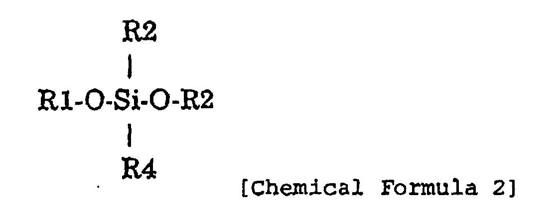
Use of such a sililation agent as a gas enables formation
of a mesoporous silica film having extremely superior moisture
resistance as well as high strength and high adhesion
characteristics. When trimethylchlorosilane is used in lieu of
dialkylkoxysilan such as that expressed by Chemical formula 2,
the moisture resistance of the film is improved further.
The composition of the precursor solution is not limited
to that described in connection with the embodiment. Under the
assumption that the solution assumes a value of 150 (100 parts
water + 50 parts ethanol), the surface active agent might be
preferably taken a value of 0.1 to 5; the silica derivative might
be preferably taken a value of 0.1 to 10 (more preferably 3.0
to 6.0); and the acid catalyst might be preferably taken a value
of 0 to 5 (more preferably 0.5 to 2.5). Use of the precursor
solution having the composition enables formation of a dielectric
film of low dielectric constant having columnar pores.
In the embodiment, cationic cetyltrimethyl ammonium
bromide [CTAB: C16(H33N+ (CH3)3Br-] is used as a surface active agent.
Naturally to say, the surface active agent might not be limited
to such an agent, and another surface active agent might be
alternatively employed.
In case of using alkali ions, such as Na ions, as catalysts,
however, it deteriorates a semiconductor material. Therefore,
eventually, use of a cationic surface active agent with an acid
catalyst might be a preferable option. In placed of HCl, an
inorganic catalyst, such as nitric acid (HNO3), sulfuric acid
(H2SO4), phosphoric acid (H3PO4), H4SO4, or the like may be used
as the acid catalyst. Alternatively, an organic acid catalyst,
such as carboxylic acid, sulfonic acid, sulfinic acid, or phenol,
may be also used.
The silica derivative used as raw material is not limited
to TMOS. Silicon alkoxide material, such as tetraethoxy silane
(TEOS), is preferably used.
Further, the water H2O/alcohol mixed solvent is used as
a solvent. However, it might be the case of only water being
used.
Moreover, although the atmosphere is used as a sintering
atmosphere, sintering may be performed in an oxygen atmosphere,
under reduced pressure, or in a nitrogen atmosphere. Preferably,
use of a foaming gas formed from a gas mixture consisting of
nitrogen and hydrogen enhances moisture resistance, thereby
enabling an attempt to reduce a leakage current.
A mixing ratio of the surface active agent, the silica
derivative, the acid catalyst, and the solvent can be changed
as required.
The preliminary crosslinking process is described as being
performed at 90°C overnight. Any temperature and any period of
time can be selected from the temperature range of 30°C to 150°C
and the time range of one to 120 hours, as required. Apreferable
temperature ranges from 60°C to 120°C, and a more preferable
temperature is 90°C.
As shown in Fig. 13, a contraction rate of the film is
measured before and after sintering while the processing time
is changed in the process for exposing TEOS to saturation vapor
pressure at 135°C. Fig. 14 shows measurement results. The
vertical axis shows a contraction rate, and the horizontal axis
shows a treatment time.
As is apparent from Fig. 14, performing the process for
exposing TEOS to the saturation vapor pressure for three hours
to three nights or thereabouts is sufficient. A preferable
temperature of the TEOS vapor is 135°C or thereabouts, and 120°C
to 180°C or thereabouts may also be preferable. As the temperature
of the TEOS vapor increases, the expected time required for
attaining an equivalent contraction inhibition effect becomes
shorter. A desirable time during which TEOS is treated in vapor
is six hours or more, more preferably 12 hours or more. Moreover,
an attempt to shorten a process time can be realized by supplying
the TEOS vapor to the container from the outside, increasing
the TEOS partial pressure, and increasing the process temperature.
The only requirement is to expose the film to the vapor of silica
derivative. Hence, the temperature is not limited to 135°C. A
temperature of 90°C or less may also be employed. The upper limit
temperature may be a temperature at which thermal decomposition
of a surface active agent starts (e.g., 200°C to 250°C) or less.
The sintering process is set to be performed for three
hours at 400°C. However, the sintering process may be performed
at 300°C to 500°C for one to five hours; preferably 350°C to 450°C.
In addition, in the embodiment, TEOS is exposed to the
saturation vapor pressure or less before being subjected to
sintering. However, the substrate may be sintered in a vapor
atmosphere of silica derivative such as TEOS. In this case,
sediments, such as oxides, may be deposited on the surface of
the substrate. In this case, the sediments should be removed
by subjecting the substrate to surface treatment after the
substrate has been sintered.
In the first embodiment, the mesoporous silica thin film
is formed by means of the spin coating method. Formation of the
mesoporous silica thin film is not limited to the spin coating
method. As shown in Fig. 6, a dip coating method may also be
employed.
Specifically, the substrate is lowered in a direction
perpendicular to a liquid surface of the prepared precursor
solution at a speed of 1 mm/s through 10 m/s until it sinks in
the solution to be left stationary in the solution for one second
to one hour.
After lapse of a desired period of time, the substrate
is pulled up in said perpendicular direction at a rate of 1 mm/s
through 10 m/s until being taken out of the solution.
As in the case of the first embodiment, the substrate is
held overnight at 90°C, whereby the silica derivative is
polymerized through a hydrolysis decomposition polycondensation
reaction. Subsequently, the substrate is heated for three to
12 hours in a saturated TEOS atmosphere at 135°C. Finally, the
substrate 1 is heated and sintered for three hours in an oxygen
atmosphere at 400°C, to thereby completely thermally decompose
and remove the surface active agent serving as a mold. Thus,
a pure mesoporous silica thin film is formed.
In addition to the foregoing method, a method for dropping
the precursor solution on the substrate is also effective as
the dip coating method.
In the first embodiment, the mesoporous silica thin film
is formed by means of applying the precursor solution through
the spin coating method. Formation of the mesoporous silica thin
film is not limited to the spin coating method. As shown in Figs.
7A and 7B, an immersion method may also be employed.
As shown in Fig. 7(a), as in the case of the previous
embodiments, the mixed precursor solution is prepared, and the
substrate 1 having the MOSFET fabricated therein is immersed
in the solution in the manner as shown in Fig. 7(b). This coated
substrate 1 is held for one night at 90°C, whereby the silica
derivative is subjected to polymerization through hydrolysis
(polycondensation reaction) (i.e., a preliminary crosslinking
process), thereby forming a mesoporous silica thin film having
cavities, the cavities being formed by taking a cyclic
self-agglomerate of the surface active agent as a mold.
Finally, as in the case of the first embodiment, the
substrate is held for two nights at 90°C, whereby the silica
derivative is polymerized through a hydrolysis decomposition
polycondensation reaction. Subsequently, the substrate is
dried for one night in a saturated TMOS atmosphere at 135°C.
Finally, the substrate 1 is heated and sintered for three hours
in an oxygen atmosphere at 400°C, to thereby completely thermally
decompose and remove the surface active agent serving as a mold.
Thus, a pure mesoporous silica thin film can be formed.
According to such a configuration, the film has a cyclic
porous structure, and hence the mechanical strength of the film
can be improved so that a highly reliable dielectric film can
be obtained. Further, the pores are oriented in parallel with
the surface of the substrate. Hence, a low dielectric constant
can be formed uniformly in the direction perpendicular to the
surface of the substrate. When the dielectric film is used as
an interlevel dielectric film, the pores have a closed structure
where no opening sections is provided either to the upper layer's
wirings or lower layer's wirings. Hence, the dielectric film
plays the role of an effective low dielectric thin film having
superior moisture resistance and enhanced reliability.
Although the embodiments have described the dielectric
film which includes apluralityof cyclicporous structure domains
including columnar pores oriented in one direction and in which
adjacent porous structure domains are oriented in different
directions, the dielectric film may be formed such that the pores
"h" are oriented in one direction over the entire surface of
the substrate, as shown in Fig. 8.
Further, as shown in Fig. 9 (b) , a structure in which the
pores "h" are oriented in a layered form is also effective. The
dielectric film is formed by increasing the concentration of
the surface active agent in the precursor solution. The other
processes are the same as those described in connection with
the first through fourth embodiments.
When the concentration of the surface active agent in the
structure shown in Fig. 4(c) is further increased, molecules
are oriented in a layered pattern, as shown in Fig. 9 (a). There
is formed a dielectric film of low dielectric constant in which
the pores "h" such as those shown in Fig. 9 (b) are oriented in
a layered form. Such a configuration realizes an attempt to
increase the pore ratio further and reduce the dielectric constant
as compared with the case of the structure having the cylindrical
pores.
At the time of formation of the precursor solution, the
structure of the resultant structural body is known to change
according to a proportion of the surface active agent to the
silica derivative.
For instance, when a molecular ratio of the surface active
agent to the silica derivative, such as CATB/TEOS, assumes a
value of 0.3 to 0.8, a three-dimensional network structure (cubic
structure) is known to be obtained. If the molecular ratio is
lower than this molecular ratio and assumes a value of 0.1 to
0.5, there is obtained a dielectric film of low dielectric constant
in which columnar pores are oriented. In contrast, when the
molecular ratio is greater than that molecular ratio and assumes
a value of 0.5 to 2, there is obtained a dielectric film of low
dielectric constant in which layered pores are oriented.
The embodiment has described the coating method using the
spinner. However, a so-called brush painting method for applying
a solution with a brush is also applicable.
The preliminary crosslinking process is performed before
the contact process for coating or immersing the substrate,
whereby the precursor solution that has initiated the preliminary
crosslinking reaction can be brought into contact with the
substrate. Further, after the precursor solution has been
brought into contact with the substrate, the preliminary
crosslinking may be performed.
In addition, the embodiment has described the interlevel
dielectric film of FRAM. However, the invention can also be
applied to various semiconductor devices using silicon; a
high-speed device including a device, such as HEMT, which uses
a compound semiconductor; a high-frequency device such as a
microwave IC; highly-integrated ferroelectric memory of MEMIS
type; and a microwave transmission line or multilayer wiring
board using a film carrier or the like.
As has been described above, according to the invention,
the surface active agent and the acid catalyst are dissolved
into a solvent at a desired mole ratio, to thereby prepare a
precursor solution. The solution is applied over the substrate.
The silica derivative is subjected to polymerization through
hydrolysis decomposition (a polycondensation reaction) (i.e.,
a preliminary crosslinking process), thereby forming a mesoporous
silica thin film having cavities, the cavities being formed by
taking a cyclic self-agglomerate of the surface active agent
as a mold. The substrate is exposed to a silica derivative
atmosphere before being subjected to sintering, and a silica
derivative is supplied. As a result, contraction of the film
is inhibited. There can be formed a sturdy mesoporous silica
thin film which takes the self-agglomerate of the surface active
agent as a mold while the cavities are maintained intact without
being fractured.
Accordingly, there can be readily obtained, with superior
controllability, a dielectric film which has extremely high
mechanical strength, an extremely high adhesion property, and
a low dielectric constant.
Claims (13)
- A method for manufacturing a semiconductor device, comprising:a process of producing a precursor solution containing a silica derivative and a surface active agent;a contact process for bringing the precursor solution into contact with the surface of a substrate;a treatment process for exposing to a silica derivative atmosphere the substrate with which the precursor solution has been brought into contact; anda process for sintering the substrate to decompose and remove the surface active agent, whereby a dielectric film is formed.
- The method for manufacturing a semiconductor device according to claim 1, wherein the treatment process includes a process for bringing the substrate into contact with silica derivative vapor at a temperature at which the surface active agent is not thermally decomposed.
- The method for manufacturing'a semiconductor device according to claim 2, wherein the treatment process is performed at a saturation vapor pressure of silica derivative vapor.
- The method for manufacturing a semiconductor device according to any one of claims 1 through 3, wherein the treatment process is performed at a temperature of 90°C to 200°C.
- The method for manufacturing a semiconductor device according to any one of claims 1 through 4, wherein the contact process is a process for coating the substrate with the precursor solution.
- The method for manufacturing a semiconductor device according to claim 5, wherein the contact process is a spin coating process for dropping the precursor solution on the substrate and spinning the substrate.
- The method for manufacturing a semiconductor device according to any one of claims 1 through 6, further comprising a preliminary crosslinking process for raising the temperature of the precursor solution to initiate a crosslinking reaction.
- The method for manufacturing a semiconductor device according to claim 1, wherein the decomposition removal process is performed in the same process as that of the treatment process, and the substrate is sintered in a silica derivative atmosphere, to thereby decompose and remove the surface active agent and form a dielectric film.
- The method for manufacturing a semiconductor device according to claim 1, wherein the silica derivative is alkylsilane halide.
- The method for manufacturing a semiconductor device according to claim 1, wherein the silica derivative is alkoxysilane halide.
- The method for manufacturing a semiconductor device according to claim 1, wherein the silica derivative is alkylalkoxysilane halide.
- The method for manufacturing a semiconductor device according to claim 1, wherein the silica derivative is alkoxysilane.
- The method for manufacturing a semiconductor device according to claim 1, wherein the silica derivative is alkylalkoxysilane.
Applications Claiming Priority (3)
| Application Number | Priority Date | Filing Date | Title |
|---|---|---|---|
| JP2001292088 | 2001-09-25 | ||
| JP2001292088 | 2001-09-25 | ||
| PCT/JP2002/009511 WO2003028097A1 (en) | 2001-09-25 | 2002-09-17 | Production method for semiconductor device |
Publications (2)
| Publication Number | Publication Date |
|---|---|
| EP1432028A1 true EP1432028A1 (en) | 2004-06-23 |
| EP1432028A4 EP1432028A4 (en) | 2010-02-24 |
Family
ID=19114122
Family Applications (1)
| Application Number | Title | Priority Date | Filing Date |
|---|---|---|---|
| EP02799472A Withdrawn EP1432028A4 (en) | 2001-09-25 | 2002-09-17 | PROCESS FOR PRODUCING SEMICONDUCTOR DEVICE |
Country Status (7)
| Country | Link |
|---|---|
| US (1) | US7166545B2 (en) |
| EP (1) | EP1432028A4 (en) |
| JP (1) | JP4170219B2 (en) |
| KR (1) | KR100879660B1 (en) |
| CN (1) | CN100343959C (en) |
| TW (1) | TW561634B (en) |
| WO (1) | WO2003028097A1 (en) |
Families Citing this family (9)
| Publication number | Priority date | Publication date | Assignee | Title |
|---|---|---|---|---|
| CN1327497C (en) * | 2002-03-04 | 2007-07-18 | 罗姆股份有限公司 | Method for forming thin film |
| JP4903373B2 (en) | 2004-09-02 | 2012-03-28 | ローム株式会社 | Manufacturing method of semiconductor device |
| JP4903374B2 (en) | 2004-09-02 | 2012-03-28 | ローム株式会社 | Manufacturing method of semiconductor device |
| JP2006120954A (en) * | 2004-10-22 | 2006-05-11 | Osaka Univ | Mesoporous thin film and manufacturing method thereof |
| TWI320401B (en) * | 2005-02-05 | 2010-02-11 | Compal Electronics Inc | Method for manufacturing a microwave substrate |
| JP4623520B2 (en) * | 2006-04-10 | 2011-02-02 | 株式会社神戸製鋼所 | Porous membrane manufacturing method and porous membrane manufactured by the method |
| US9272271B2 (en) * | 2007-09-19 | 2016-03-01 | General Electric Company | Manufacture of catalyst compositions and systems |
| US8530369B2 (en) * | 2007-09-19 | 2013-09-10 | General Electric Company | Catalyst and method of manufacture |
| JPWO2022137985A1 (en) | 2020-12-24 | 2022-06-30 |
Family Cites Families (13)
| Publication number | Priority date | Publication date | Assignee | Title |
|---|---|---|---|---|
| JP2823878B2 (en) * | 1989-03-09 | 1998-11-11 | 触媒化成工業株式会社 | Method for manufacturing semiconductor integrated circuit |
| KR960006961B1 (en) | 1991-09-13 | 1996-05-25 | 니뽄 덴끼 가부시끼가이샤 | Wiring structure and insulating film formation method of semiconductor device and surface protection film formation method thereof |
| JP2792335B2 (en) * | 1992-05-27 | 1998-09-03 | 日本電気株式会社 | Method for manufacturing semiconductor device |
| JPH0770534B2 (en) | 1993-01-11 | 1995-07-31 | 日本電気株式会社 | Method for manufacturing semiconductor device |
| JPH06349817A (en) * | 1993-06-14 | 1994-12-22 | Kawasaki Steel Corp | Method for manufacturing semiconductor device |
| US5492736A (en) * | 1994-11-28 | 1996-02-20 | Air Products And Chemicals, Inc. | Fluorine doped silicon oxide process |
| CN1062836C (en) * | 1997-09-18 | 2001-03-07 | 复旦大学 | Method for preparing MCM-48 mesonore molecular sieve using anionic-cationic surfactant as template agent |
| US5858457A (en) * | 1997-09-25 | 1999-01-12 | Sandia Corporation | Process to form mesostructured films |
| JP3297998B2 (en) | 1998-02-26 | 2002-07-02 | 住友金属工業株式会社 | Melting method of high clean ultra low carbon steel |
| CN1101339C (en) * | 1998-07-01 | 2003-02-12 | 复旦大学 | Composite medium and micro porous molecular sieve and synthesis method therefor |
| US6329017B1 (en) * | 1998-12-23 | 2001-12-11 | Battelle Memorial Institute | Mesoporous silica film from a solution containing a surfactant and methods of making same |
| IL143589A0 (en) * | 1998-12-23 | 2002-04-21 | Battelle Memorial Institute | Mesoporous silica film from a solution containing a surfactant and methods of making same |
| DE60138327D1 (en) * | 2000-02-28 | 2009-05-28 | Jsr Corp | Film-making composition, film-forming method and silica-based film |
-
2002
- 2002-09-16 TW TW091121101A patent/TW561634B/en not_active IP Right Cessation
- 2002-09-17 WO PCT/JP2002/009511 patent/WO2003028097A1/en not_active Ceased
- 2002-09-17 US US10/490,767 patent/US7166545B2/en not_active Expired - Fee Related
- 2002-09-17 CN CNB028187709A patent/CN100343959C/en not_active Expired - Fee Related
- 2002-09-17 KR KR1020047004316A patent/KR100879660B1/en not_active Expired - Fee Related
- 2002-09-17 JP JP2003531523A patent/JP4170219B2/en not_active Expired - Fee Related
- 2002-09-17 EP EP02799472A patent/EP1432028A4/en not_active Withdrawn
Also Published As
| Publication number | Publication date |
|---|---|
| JP4170219B2 (en) | 2008-10-22 |
| US7166545B2 (en) | 2007-01-23 |
| CN1559083A (en) | 2004-12-29 |
| TW561634B (en) | 2003-11-11 |
| KR20040039410A (en) | 2004-05-10 |
| KR100879660B1 (en) | 2009-01-20 |
| CN100343959C (en) | 2007-10-17 |
| JPWO2003028097A1 (en) | 2005-01-13 |
| WO2003028097A1 (en) | 2003-04-03 |
| EP1432028A4 (en) | 2010-02-24 |
| US20050003678A1 (en) | 2005-01-06 |
Similar Documents
| Publication | Publication Date | Title |
|---|---|---|
| EP1482567A1 (en) | Light-emitting device comprising led chip and method for manufacturing this device | |
| US6699797B1 (en) | Method of fabrication of low dielectric constant porous metal silicate films | |
| US20070164437A1 (en) | Semiconductor device and method of manufacturing the same | |
| US7166545B2 (en) | Production method for semiconductor device | |
| JP4391240B2 (en) | Thin film forming method and semiconductor device | |
| KR100645654B1 (en) | Semiconductor device and manufacturing method thereof | |
| KR100622713B1 (en) | Semiconductor device and manufacturing method | |
| CN100369216C (en) | Semiconductor device and manufacturing method thereof | |
| JP2003017483A (en) | Semiconductor device and method of manufacturing the same | |
| JP2003017486A (en) | Semiconductor device and method of manufacturing the same | |
| KR20000027388A (en) | Method for manufacturing bpsg interlayer dielectric of semiconductor devices | |
| JP2003017484A (en) | Semiconductor device and method for manufacturing the same | |
| JP2003017487A (en) | Semiconductor device and method for manufacturing the same | |
| JPH04147625A (en) | Manufacture of semiconductor device |
Legal Events
| Date | Code | Title | Description |
|---|---|---|---|
| PUAI | Public reference made under article 153(3) epc to a published international application that has entered the european phase |
Free format text: ORIGINAL CODE: 0009012 |
|
| 17P | Request for examination filed |
Effective date: 20040325 |
|
| AK | Designated contracting states |
Kind code of ref document: A1 Designated state(s): AT BE CH CY DE DK ES FI FR GB GR IE IT LI LU MC NL PT SE TR |
|
| A4 | Supplementary search report drawn up and despatched |
Effective date: 20100127 |
|
| STAA | Information on the status of an ep patent application or granted ep patent |
Free format text: STATUS: THE APPLICATION IS DEEMED TO BE WITHDRAWN |
|
| 18D | Application deemed to be withdrawn |
Effective date: 20100401 |