EP1431036A1 - Electrostatically actuated drop ejector - Google Patents
Electrostatically actuated drop ejector Download PDFInfo
- Publication number
- EP1431036A1 EP1431036A1 EP03078885A EP03078885A EP1431036A1 EP 1431036 A1 EP1431036 A1 EP 1431036A1 EP 03078885 A EP03078885 A EP 03078885A EP 03078885 A EP03078885 A EP 03078885A EP 1431036 A1 EP1431036 A1 EP 1431036A1
- Authority
- EP
- European Patent Office
- Prior art keywords
- electrode
- emission device
- chamber
- drop
- ejecting
- Prior art date
- Legal status (The legal status is an assumption and is not a legal conclusion. Google has not performed a legal analysis and makes no representation as to the accuracy of the status listed.)
- Granted
Links
- 239000007788 liquid Substances 0.000 claims abstract description 48
- 239000003989 dielectric material Substances 0.000 claims abstract description 11
- 230000007423 decrease Effects 0.000 claims abstract description 3
- 238000002161 passivation Methods 0.000 claims description 7
- 239000004020 conductor Substances 0.000 claims description 5
- 238000007641 inkjet printing Methods 0.000 claims description 3
- 239000000976 ink Substances 0.000 description 15
- 239000010410 layer Substances 0.000 description 13
- 230000007246 mechanism Effects 0.000 description 7
- 229910021420 polycrystalline silicon Inorganic materials 0.000 description 7
- 229920005591 polysilicon Polymers 0.000 description 7
- 239000000463 material Substances 0.000 description 4
- 239000012528 membrane Substances 0.000 description 4
- 239000012530 fluid Substances 0.000 description 3
- 239000011521 glass Substances 0.000 description 3
- XUIMIQQOPSSXEZ-UHFFFAOYSA-N Silicon Chemical compound [Si] XUIMIQQOPSSXEZ-UHFFFAOYSA-N 0.000 description 2
- 230000005684 electric field Effects 0.000 description 2
- 239000010408 film Substances 0.000 description 2
- 238000009413 insulation Methods 0.000 description 2
- 229910052710 silicon Inorganic materials 0.000 description 2
- 239000010703 silicon Substances 0.000 description 2
- 239000000758 substrate Substances 0.000 description 2
- 239000010409 thin film Substances 0.000 description 2
- 238000013022 venting Methods 0.000 description 2
- 229910052581 Si3N4 Inorganic materials 0.000 description 1
- 230000015572 biosynthetic process Effects 0.000 description 1
- 230000015556 catabolic process Effects 0.000 description 1
- 230000037406 food intake Effects 0.000 description 1
- 230000002209 hydrophobic effect Effects 0.000 description 1
- 238000004519 manufacturing process Methods 0.000 description 1
- 230000005499 meniscus Effects 0.000 description 1
- 150000004767 nitrides Chemical class 0.000 description 1
- 238000005381 potential energy Methods 0.000 description 1
- 238000007639 printing Methods 0.000 description 1
- HQVNEWCFYHHQES-UHFFFAOYSA-N silicon nitride Chemical compound N12[Si]34N5[Si]62N3[Si]51N64 HQVNEWCFYHHQES-UHFFFAOYSA-N 0.000 description 1
- 239000002356 single layer Substances 0.000 description 1
- 238000012876 topography Methods 0.000 description 1
Images




Classifications
-
- B—PERFORMING OPERATIONS; TRANSPORTING
- B41—PRINTING; LINING MACHINES; TYPEWRITERS; STAMPS
- B41J—TYPEWRITERS; SELECTIVE PRINTING MECHANISMS, i.e. MECHANISMS PRINTING OTHERWISE THAN FROM A FORME; CORRECTION OF TYPOGRAPHICAL ERRORS
- B41J2/00—Typewriters or selective printing mechanisms characterised by the printing or marking process for which they are designed
- B41J2/005—Typewriters or selective printing mechanisms characterised by the printing or marking process for which they are designed characterised by bringing liquid or particles selectively into contact with a printing material
- B41J2/01—Ink jet
- B41J2/135—Nozzles
- B41J2/14—Structure thereof only for on-demand ink jet heads
- B41J2/14314—Structure of ink jet print heads with electrostatically actuated membrane
Definitions
- the present invention relates generally to micro-electromechanical (MEM) drop-on-demand liquid emission devices such as, for example, ink jet printers, and more particularly such devices which employ an electrostatic actuator for driving liquid from the device.
- MEM micro-electromechanical
- U.S. Patent No. 6,345,884 teaches a device having an electrostatically deformable membrane with an ink refill hole in the membrane. An electric field applied across the ink deflects the membrane and expels an ink drop.
- U.S. Patent No. 6,357,865 by J. Kubby et al. teaches a surface micro-machined drop ejector made with deposited polysilicon layers. Drops from an ink cavity are expelled through an orifice in an upper polysilicon layer when a lower polysilicon layer is first pulled down to contact a conductor and is subsequently released.
- U.S. Patent No. 6,235,212 provides a vented space between a distortable diaphragm and the opposed, fixed electrode.
- the vent is a very thin slot around the perimeter of the device. Because the mechanism relies on hydrophobic layers between the electrodes to keep the chamber clear of fluid, the cross-sectional area of the perimeter vent gap is by necessity insufficient to provide adequate venting.
- the thickness of the vent is given in the patent as 0.5 ⁇ m.
- the cross sectional area of the vent would be only about 120 ⁇ m 2 ; as calculated below:
- the perimeter of the vent would be approximately 480 ⁇ m, for an area-to-perimeter ratio of 0.25 ⁇ m. This would be a very slowly venting device; and therefore would be slow to fire and refill.
- a 20 ⁇ m diameter vent hole in the fixed electrode provides an area of 300 ⁇ m 2 with a perimeter of only 60 ⁇ m for an area-to-perimeter ratio of 5 ⁇ m.
- the present invention would be able to actuate and refill approximately 20 times faster than would the device disclosed in U.S. Patent No. 6,235,212.
- an emission device for ejecting a liquid drop includes a first chamber of variable volume adapted to receive a liquid.
- the chamber has a nozzle orifice through which a drop of received liquid can be emitted.
- An electrically addressable, deformable electrode is associated with the first chamber such that movement of the deformable electrode in a first direction increases the first chamber's volume to draw liquid into the first chamber and movement of the deformable electrode in a second direction decreases the first chamber's volume to emit a drop of liquid from the first chamber through the nozzle orifice.
- a fixed electrode opposes to the deformable electrode to define a second chamber there between such that control of relative voltage differences between the movable and the fixed electrodes selectively moves the deformable electrode in one of the first and second directions.
- the variable volume contains a dielectric material and is vented to a source of such dielectric material through an opening of predetermined cross-sectional area in the fixed electrode.
- the ratio of the cross-sectional area of the opening to the perimeter of the fixed electrode is greater than 0.25 ⁇ m, and is preferably about 5 ⁇ m.
- the present invention provides a novel drop-on-demand liquid emission device.
- the most familiar of such devices are used as printheads in ink jet printing systems.
- Many other applications are emerging which make use of devices similar to ink jet printheads, but which emit liquids (other than inks) that need to be finely metered and deposited with high spatial precision.
- FIG. 1 shows a schematic representation of a drop-on-demand liquid emission device 10, such as an ink jet printer, which may be operated according to the present invention.
- the system includes a source 12 of data (say, image data) which provides signals that are interpreted by a controller 14 as being commands to emit drops.
- Controller 14 outputs signals to a source 16 of electrical energy pulses which are inputted to a drop-on-demand liquid emission device such as an ink jet printer 18.
- Drop-on-demand liquid emission device 10 includes a plurality of electrostatic drop ejection mechanisms 20.
- FIG. 2 is a top view of a portion of drop ejection mechanism 20 of FIG. 1 formed according to a preferred embodiment of the present invention. In this and the following figures, the structure continues to be illustrated in schematic form.
- FIGS. 3-5 are top plan views of nozzle plate 22, showing several alternative embodiments of layout patterns for the several nozzle orifices 24 of a print head. Note that in FIGS. 2 and 3, the interior surface of walls 26 are annular, while in FIG. 5, walls 26 form rectangular chambers. Other shapes are of course possible, and these drawings are merely intended to convey the understanding that alternatives are possible within the spirit and scope of the present invention.
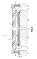
- FIGS. 6, 7, and 8 are cross-sectional views of one of the plurality of electrostatically actuated drop ejection mechanisms 20 taken along line I-I', II-II', and III-III', respectively, of FIG. 2.
- a nozzle orifice 24 is formed in a nozzle plate 22 for each mechanism 20.
- the thickness of nozzle plate 22 is determined to constrain the plate against flexing, as any deformation represents a reduction in the drop ejection energy, and may inhibit drop formation.
- the wall may comprise a single material or may comprise a stack of material layers, as shown in FIG. 6.
- a portion of deformable electrode 28 is sealingly attached to outer wall 25 to define a liquid chamber 30 adapted to receive the liquid, such as for example ink, to be ejected from nozzle orifice 24.
- the liquid is drawn into chamber 30 through one or more refill ports 32 from a supply, not shown, typically forming a meniscus in the nozzle orifice. Ports 32 are sized as discussed below.
- Dielectric material fills the region on the side of deformable electrode 28 opposed to chamber 30.
- the dielectric material is preferably air or other dielectric gas, although a dielectric liquid may be used.
- deformable electrode 28 is made of a somewhat flexible conductive material such as polysilicon, or a combination of layers having a central conductive layer surrounded by an upper and lower insulating layer.
- an alternative electrode 28 comprises a thin film of polysilicon stacked between two thin films of silicon nitride, each film for example, being one micron thick. In the latter case, the nitride acts to stiffen the polysilicon film and to insulate it from liquid in the chamber 30.
- Addressable electrode 28 is preferably at least partially flexible and is spaced from a fixed electrode 34 such that the two electrodes are generally axially aligned with nozzle orifice 24.
- Fixed electrode 34 is preferably made from a conductive central body, and is rigidly attached to walls 26.
- a first passivation layer 35 provides insulation of electrode 34 from the structural supports 44, while a second passivation layer 36 provides insulation of fixed electrode 34 from deformable electrode 28 during pulldown, when the two electrodes will be brought into mechanical contact.
- the thicknesses of passivation layers 35 and 36 are determined by the breakdown voltages of the passivation materials and the voltages applied when the electrodes are brought into contact.
- deformable electrode 28 is in contact with the liquid in chamber 30, it may be preferable that fixed electrode 34 is powered while deformable electrode 28 remains at some reference voltage referred to as ground or zero. Deformable electrode 28 deforms and comes into mechanical contact with fixed electrode 34. The first passivation layer 35 between the two electrodes prevents electrical discharge. Since deformable electrode 28 forms a wall portion of liquid chamber 30 behind the nozzle orifice, movement of deformable electrode 28 away from nozzle plate 22 expands the chamber 30, drawing liquid into the expanding chamber through ports 32.
- deformable electrode 28 is de-energized, that is, the potential difference between electrodes 28 and 34 is made zero.
- Deformable electrode 28 begins to move from the position illustrated in FIG. 9 toward the position illustrated in FIG. 10 under the sole force of stored elastic potential energy in the system. Still referring to FIG. 10, this action pressurizes the liquid in chamber 30 behind nozzle orifice 24, causing a drop to be ejected from the nozzle orifice.
- ports 32 and flow restrictors 38 should be properly sized to present sufficiently low flow resistance so that filling of chamber 30 is not significantly impeded when deformable electrode 28 is energized, and yet present sufficiently high resistance to the back flow of liquid through the port during drop ejection.
- Flow restrictor 38 can be sized to inhibit ingestion of the ambient environment during this step.
- Electrodes 28 and 34 of FIG. 6 are anchored to outer wall 26 by structural supports 44. Both outer wall 26 and structural supports 44 may either comprise a single layer or comprise a stack of material layers as shown in FIG. 7.
- a second fluid path 42 shown in FIGS. 6-11 allows the dielectric material in a chamber below electrode 34 to flow into and out of a dielectric material reservoir (not shown).
- the dielectric material is air, and the ambient atmosphere performs the function of a dielectric material reservoir.
- Fluid path 42 forms a vent opening of predetermined cross-sectional area in fixed electrode 34. The ratio of the cross-sectional area of the vent opening to the perimeter of fixed electrode 34 being greater than 0.25 ⁇ m, and preferably about 5 ⁇ m.
- FIG. 11 illustrates and alternative embodiment of the present invention.
- the drawing is taken as if along line I-I' of FIG. 2.
- nozzle plate 22 is formed separately from the rest of the device and is then bonded to the device. This eliminates some of the topography in the nozzle plate level.
Landscapes
- Particle Formation And Scattering Control In Inkjet Printers (AREA)
Abstract
Description
- The present invention relates generally to micro-electromechanical (MEM) drop-on-demand liquid emission devices such as, for example, ink jet printers, and more particularly such devices which employ an electrostatic actuator for driving liquid from the device.
- Drop-on-demand liquid emission devices with electrostatic actuators are known for ink printing systems. U.S. Patents No. 5,644,341 and No. 5,668,579, which issued to Fuji et al. on July 1, 1997 and September 16, 1997, respectively, disclose such devices having electrostatic actuators composed of-a single diaphragm and opposed electrode. The diaphragm is distorted by application of a voltage differential between two electrodes. Relaxation of the diaphragm expels an ink droplet from the device. Other devices that operate on the principle of electrostatic attraction are disclosed in U.S. Patents No. 5,739,831, No. 6,127,198, and No. 6,318,841; and in U.S. Publication No. 2001/0023523.
- U.S. Patent No. 6,345,884 teaches a device having an electrostatically deformable membrane with an ink refill hole in the membrane. An electric field applied across the ink deflects the membrane and expels an ink drop.
- IEEE Conference Proceeding "MEMS 1998," held January 25-29, 2002 in Heidelberg, Germany, entitled "A Low Power, Small, Electrostatically-Driven Commercial Inkjet Head" by S. Darmisuki, et al., discloses a head made by anodically bonding three substrates, two of glass and one of silicon, to form an ink ejector. Drops from an ink cavity are expelled through an orifice in the top glass plate when a membrane formed in the silicon substrate is first pulled down to contact a conductor on the lower glass plate and subsequently released. There is no electric field in the ink. The device occupies a large area and is expensive to manufacture.
- U.S. Patent No. 6,357,865 by J. Kubby et al. teaches a surface micro-machined drop ejector made with deposited polysilicon layers. Drops from an ink cavity are expelled through an orifice in an upper polysilicon layer when a lower polysilicon layer is first pulled down to contact a conductor and is subsequently released.
- In above-mentioned U.S. Patent No. 6,127,198, air trapped between the distortable diaphragm and the opposed, fixed electrode is compressed when a voltage is applied to the electrode. The air chamber must have a relatively large volume to accommodate the compressed air; reducing the number of ejection nozzles that can be located in a given area.
- U.S. Patent No. 6,235,212 provides a vented space between a distortable diaphragm and the opposed, fixed electrode. The vent is a very thin slot around the perimeter of the device. Because the mechanism relies on hydrophobic layers between the electrodes to keep the chamber clear of fluid, the cross-sectional area of the perimeter vent gap is by necessity insufficient to provide adequate venting. The thickness of the vent is given in the patent as 0.5µm. Even assuming that the entire perimeter on an 80µm device were vented (although it is likely that, say, 25% of the perimeter would be used to anchor the device), the cross sectional area of the vent would be only about 120µm2; as calculated below:The perimeter of the vent would be approximately 480µm, for an area-to-perimeter ratio of 0.25µm. This would be a very slowly venting device; and therefore would be slow to fire and refill.

- It is an object of the present invention to provide a micro-electromechanical (MEM) drop-on-demand liquid emission device of the type discussed that is able to actuate and refill rapidly by providing a vent hole in the rear of the fixed electrode. As an example, a 20 µm diameter vent hole in the fixed electrode provides an area of 300 µm2 with a perimeter of only 60 µm for an area-to-perimeter ratio of 5 µm. Thus, all other things being equal, the present invention would be able to actuate and refill approximately 20 times faster than would the device disclosed in U.S. Patent No. 6,235,212.
- According to a feature of the present invention, an emission device for ejecting a liquid drop includes a first chamber of variable volume adapted to receive a liquid. The chamber has a nozzle orifice through which a drop of received liquid can be emitted. An electrically addressable, deformable electrode is associated with the first chamber such that movement of the deformable electrode in a first direction increases the first chamber's volume to draw liquid into the first chamber and movement of the deformable electrode in a second direction decreases the first chamber's volume to emit a drop of liquid from the first chamber through the nozzle orifice. A fixed electrode, of predetermined perimeter, opposes to the deformable electrode to define a second chamber there between such that control of relative voltage differences between the movable and the fixed electrodes selectively moves the deformable electrode in one of the first and second directions. The variable volume contains a dielectric material and is vented to a source of such dielectric material through an opening of predetermined cross-sectional area in the fixed electrode. The ratio of the cross-sectional area of the opening to the perimeter of the fixed electrode is greater than 0.25 µm, and is preferably about 5 µm.
- FIG. 1 is a schematic illustration of a drop-on-demand liquid emission device according to the present invention;
- FIG. 2 is a top sectional view of a portion of the drop-on-demand liquid emission device of FIG. 1;
- FIGS. 3-5 are top plan views of alternative embodiments of a nozzle plate of the drop-on-demand liquid emission device of FIGS. 1 and 2;
- FIG. 6 is a cross-sectional view of the drop-on-demand liquid emission device of FIG. 1 taken along line I-I' of FIG. 2 with the mechanism at rest;
- FIG. 7 is a cross-sectional view of the drop-on-demand liquid emission device of FIG. 1 taken along line II-II' of FIG. 2;
- FIG. 8 is a cross-sectional view of the drop-on-demand liquid emission device of FIG. 1 taken along line III-III' of FIG. 2;
- FIG. 9 is a cross-sectional view similar to FIG. 6 of the drop-on-demand liquid emission device of FIG. 2 shown in a first actuation stage;
- FIG. 10 is a cross-sectional view similar to FIG. 9 shown in a second actuation stage; and
- FIG. 11 is a cross-sectional view of another embodiment of the drop-on-demand liquid emission device of FIG. 1 taken along line I-I' of FIG. 2.
-
- As described in detail herein below, the present invention provides a novel drop-on-demand liquid emission device. The most familiar of such devices are used as printheads in ink jet printing systems. Many other applications are emerging which make use of devices similar to ink jet printheads, but which emit liquids (other than inks) that need to be finely metered and deposited with high spatial precision.
- FIG. 1 shows a schematic representation of a drop-on-demand
liquid emission device 10, such as an ink jet printer, which may be operated according to the present invention. The system includes asource 12 of data (say, image data) which provides signals that are interpreted by acontroller 14 as being commands to emit drops.Controller 14 outputs signals to asource 16 of electrical energy pulses which are inputted to a drop-on-demand liquid emission device such as anink jet printer 18. - Drop-on-demand
liquid emission device 10 includes a plurality of electrostaticdrop ejection mechanisms 20. FIG. 2 is a top view of a portion ofdrop ejection mechanism 20 of FIG. 1 formed according to a preferred embodiment of the present invention. In this and the following figures, the structure continues to be illustrated in schematic form. - FIGS. 3-5 are top plan views of
nozzle plate 22, showing several alternative embodiments of layout patterns for theseveral nozzle orifices 24 of a print head. Note that in FIGS. 2 and 3, the interior surface ofwalls 26 are annular, while in FIG. 5,walls 26 form rectangular chambers. Other shapes are of course possible, and these drawings are merely intended to convey the understanding that alternatives are possible within the spirit and scope of the present invention. - FIGS. 6, 7, and 8 are cross-sectional views of one of the plurality of electrostatically actuated
drop ejection mechanisms 20 taken along line I-I', II-II', and III-III', respectively, of FIG. 2. Anozzle orifice 24 is formed in anozzle plate 22 for eachmechanism 20. The thickness ofnozzle plate 22 is determined to constrain the plate against flexing, as any deformation represents a reduction in the drop ejection energy, and may inhibit drop formation. A wall orwalls 26, which carry an electrically addressabledeformable electrode 28, bound eachdrop ejection mechanism 20. The wall may comprise a single material or may comprise a stack of material layers, as shown in FIG. 6. - A portion of
deformable electrode 28 is sealingly attached toouter wall 25 to define aliquid chamber 30 adapted to receive the liquid, such as for example ink, to be ejected fromnozzle orifice 24. The liquid is drawn intochamber 30 through one ormore refill ports 32 from a supply, not shown, typically forming a meniscus in the nozzle orifice.Ports 32 are sized as discussed below. Dielectric material fills the region on the side ofdeformable electrode 28 opposed tochamber 30. The dielectric material is preferably air or other dielectric gas, although a dielectric liquid may be used. - Typically,
deformable electrode 28 is made of a somewhat flexible conductive material such as polysilicon, or a combination of layers having a central conductive layer surrounded by an upper and lower insulating layer. For example analternative electrode 28 comprises a thin film of polysilicon stacked between two thin films of silicon nitride, each film for example, being one micron thick. In the latter case, the nitride acts to stiffen the polysilicon film and to insulate it from liquid in thechamber 30. -
Addressable electrode 28 is preferably at least partially flexible and is spaced from a fixedelectrode 34 such that the two electrodes are generally axially aligned withnozzle orifice 24. - Fixed
electrode 34 is preferably made from a conductive central body, and is rigidly attached towalls 26. Afirst passivation layer 35 provides insulation ofelectrode 34 from thestructural supports 44, while asecond passivation layer 36 provides insulation of fixedelectrode 34 fromdeformable electrode 28 during pulldown, when the two electrodes will be brought into mechanical contact. The thicknesses of passivation layers 35 and 36 are determined by the breakdown voltages of the passivation materials and the voltages applied when the electrodes are brought into contact. - Referring to FIG. 9, to eject a drop, voltage difference is applied between the polysilicon portion of
deformable electrode 28 and the conductive portion of fixedelectrode 34. Sincedeformable electrode 28 is in contact with the liquid inchamber 30, it may be preferable that fixedelectrode 34 is powered whiledeformable electrode 28 remains at some reference voltage referred to as ground or zero.Deformable electrode 28 deforms and comes into mechanical contact with fixedelectrode 34. Thefirst passivation layer 35 between the two electrodes prevents electrical discharge. Sincedeformable electrode 28 forms a wall portion ofliquid chamber 30 behind the nozzle orifice, movement ofdeformable electrode 28 away fromnozzle plate 22 expands thechamber 30, drawing liquid into the expanding chamber throughports 32. - Subsequently (say, several microseconds later)
deformable electrode 28 is de-energized, that is, the potential difference betweenelectrodes Deformable electrode 28 begins to move from the position illustrated in FIG. 9 toward the position illustrated in FIG. 10 under the sole force of stored elastic potential energy in the system. Still referring to FIG. 10, this action pressurizes the liquid inchamber 30 behindnozzle orifice 24, causing a drop to be ejected from the nozzle orifice. To optimize both refill and drop ejection,ports 32 andflow restrictors 38 should be properly sized to present sufficiently low flow resistance so that filling ofchamber 30 is not significantly impeded whendeformable electrode 28 is energized, and yet present sufficiently high resistance to the back flow of liquid through the port during drop ejection. Asdeformable electrode 28 moves away fromnozzle plate 22 to draw liquid into the expanding chamber throughports 32, some ambient environment is drawn in throughnozzle orifice 24. Flow restrictor 38 can be sized to inhibit ingestion of the ambient environment during this step. - Referring again to FIG. 2, during operation, electrical signals are sent via
electrical leads 40 toelectrodes outer wall 26 bystructural supports 44. Bothouter wall 26 andstructural supports 44 may either comprise a single layer or comprise a stack of material layers as shown in FIG. 7. - A
second fluid path 42 shown in FIGS. 6-11 allows the dielectric material in a chamber belowelectrode 34 to flow into and out of a dielectric material reservoir (not shown). In the preferred embodiment, the dielectric material is air, and the ambient atmosphere performs the function of a dielectric material reservoir.Fluid path 42 forms a vent opening of predetermined cross-sectional area in fixedelectrode 34. The ratio of the cross-sectional area of the vent opening to the perimeter of fixedelectrode 34 being greater than 0.25 µm, and preferably about 5 µm. - FIG. 11 illustrates and alternative embodiment of the present invention. The drawing is taken as if along line I-I' of FIG. 2. In this embodiment,
nozzle plate 22 is formed separately from the rest of the device and is then bonded to the device. This eliminates some of the topography in the nozzle plate level.
Claims (10)
- An emission device for ejecting a liquid drop, said device having:a first chamber (30) of variable volume adapted to receive a liquid and having a nozzle orifice (24) through which a drop of received liquid can be emitted; an electrically addressable, deformable electrode (28) associated with the first chamber (30) such that movement of the deformable electrode (28) in a first direction increases the first chamber's volume to draw liquid into the first chamber and movement of the deformable electrode (28) in a second direction decreases the first chamber's volume to emit a drop of liquid from the first chamber through the nozzle orifice; and a fixed electrode (34), of predetermined perimeter, opposed to the deformable electrode (28) and defining a second chamber there between such that control of relative voltage differences between the movable and the fixed electrodes (28, 30) selectively moves the deformable electrode in one of said first and second directions, characterized by said variable volume containing a dielectric material and being vented to a source of such dielectric material through an opening of predetermined cross-sectional area in the fixed electrode, the ratio of the cross-sectional area of said opening to the perimeter of the fixed electrode being greater than 0.25 µm.
- An emission device for ejecting a liquid drop as defined in Claim 1, wherein the deformable electrode is formed of a flexible conductive material.
- An emission device for ejecting a liquid drop as defined in Claim 1, wherein the deformable electrode is formed of a central conductive layer surrounded by opposed insulating layers.
- An emission device for ejecting a liquid drop as defined in Claim 1, wherein the fixed electrode is formed of a conductive body and a passivation layer to insulate the fixed electrode from the deformable electrode.
- An emission device for ejecting a liquid drop as defined in Claim 1, wherein the emission device is a print head of an ink jet printing system.
- An emission device for ejecting a liquid drop as defined in Claim 1, wherein the ratio of the cross-sectional area of said opening to the perimeter of the fixed electrode about 5 µm.
- An emission device for ejecting a liquid drop as defined in Claim 6, wherein the deformable electrode is formed of a flexible conductive material.
- An emission device for ejecting a liquid drop as defined in Claim 6, wherein the deformable electrode is formed of a central conductive layer surrounded by opposed insulating layers.
- An emission device for ejecting a liquid drop as defined in Claim 6, wherein the fixed electrode is formed of a conductive body and a passivation layer to insulate the fixed electrode from the deformable electrode.
- An emission device for ejecting a liquid drop as defined in Claim 6, wherein the emission device is a print head of an ink jet printing system.
Applications Claiming Priority (2)
| Application Number | Priority Date | Filing Date | Title |
|---|---|---|---|
| US325205 | 2002-12-18 | ||
| US10/325,205 US6874867B2 (en) | 2002-12-18 | 2002-12-18 | Electrostatically actuated drop ejector |
Publications (2)
| Publication Number | Publication Date |
|---|---|
| EP1431036A1 true EP1431036A1 (en) | 2004-06-23 |
| EP1431036B1 EP1431036B1 (en) | 2008-01-16 |
Family
ID=32393093
Family Applications (1)
| Application Number | Title | Priority Date | Filing Date |
|---|---|---|---|
| EP03078885A Expired - Lifetime EP1431036B1 (en) | 2002-12-18 | 2003-12-08 | Electrostatically actuated drop ejector |
Country Status (4)
| Country | Link |
|---|---|
| US (1) | US6874867B2 (en) |
| EP (1) | EP1431036B1 (en) |
| JP (1) | JP2004195967A (en) |
| DE (1) | DE60318677T2 (en) |
Families Citing this family (3)
| Publication number | Priority date | Publication date | Assignee | Title |
|---|---|---|---|---|
| JP4617765B2 (en) * | 2004-08-17 | 2011-01-26 | ソニー株式会社 | FUNCTIONAL ELEMENT AND ITS MANUFACTURING METHOD, FLUID DISCHARGE DEVICE, AND PRINTING DEVICE |
| TWI250629B (en) | 2005-01-12 | 2006-03-01 | Ind Tech Res Inst | Electronic package and fabricating method thereof |
| US7905573B2 (en) * | 2007-06-19 | 2011-03-15 | Ricoh Company, Ltd. | Liquid ejection head with nozzle plate deformed by heat and image forming apparatus including the liquid election head |
Citations (5)
| Publication number | Priority date | Publication date | Assignee | Title |
|---|---|---|---|---|
| JPH1086364A (en) * | 1996-09-12 | 1998-04-07 | Ricoh Co Ltd | Ink jet recording head and method of manufacturing the same |
| US5764258A (en) * | 1994-08-20 | 1998-06-09 | Eastman Kodak Company | Print head with integrated pump |
| JPH11291485A (en) * | 1998-04-10 | 1999-10-26 | Minolta Co Ltd | Ink jet head |
| US6235212B1 (en) * | 1997-07-15 | 2001-05-22 | Silverbrook Research Pty Ltd | Method of manufacture of an electrostatic ink jet printer |
| US6332669B1 (en) * | 1997-06-05 | 2001-12-25 | Ricoh Company, Ltd. | Ink jet head including vibration plate and electrode substrate |
Family Cites Families (16)
| Publication number | Priority date | Publication date | Assignee | Title |
|---|---|---|---|---|
| US4908679A (en) * | 1981-01-23 | 1990-03-13 | National Semiconductor Corporation | Low resistance Schottky diode on polysilicon/metal-silicide |
| JPH0828427B2 (en) * | 1988-09-14 | 1996-03-21 | 三菱電機株式会社 | Semiconductor device and manufacturing method thereof |
| US5013693A (en) | 1989-02-16 | 1991-05-07 | Wisconsin Alumni Research Foundation | Formation of microstructures with removal of liquid by freezing and sublimation |
| US5668579A (en) * | 1993-06-16 | 1997-09-16 | Seiko Epson Corporation | Apparatus for and a method of driving an ink jet head having an electrostatic actuator |
| US5644341A (en) * | 1993-07-14 | 1997-07-01 | Seiko Epson Corporation | Ink jet head drive apparatus and drive method, and a printer using these |
| JP3303901B2 (en) * | 1994-09-16 | 2002-07-22 | セイコーエプソン株式会社 | Electric field drive type ink jet recording head and driving method thereof |
| US5907791A (en) * | 1996-04-25 | 1999-05-25 | Lucent Technologies Inc. | Method of making semiconductor devices by patterning a wafer having a non-planar surface |
| US5804084A (en) * | 1996-10-11 | 1998-09-08 | Sandia Corporation | Use of chemical mechanical polishing in micromachining |
| US5890745A (en) * | 1997-01-29 | 1999-04-06 | The Board Of Trustees Of The Leland Stanford Junior University | Micromachined fluidic coupler |
| US6082208A (en) * | 1998-04-01 | 2000-07-04 | Sandia Corporation | Method for fabricating five-level microelectromechanical structures and microelectromechanical transmission formed |
| US6357865B1 (en) * | 1998-10-15 | 2002-03-19 | Xerox Corporation | Micro-electro-mechanical fluid ejector and method of operating same |
| US6318841B1 (en) * | 1998-10-15 | 2001-11-20 | Xerox Corporation | Fluid drop ejector |
| US6662448B2 (en) * | 1998-10-15 | 2003-12-16 | Xerox Corporation | Method of fabricating a micro-electro-mechanical fluid ejector |
| US6127198A (en) * | 1998-10-15 | 2000-10-03 | Xerox Corporation | Method of fabricating a fluid drop ejector |
| US6174820B1 (en) * | 1999-02-16 | 2001-01-16 | Sandia Corporation | Use of silicon oxynitride as a sacrificial material for microelectromechanical devices |
| KR20010045309A (en) * | 1999-11-04 | 2001-06-05 | 윤종용 | Ink jetting apparatus and a method for manufacturing the same |
-
2002
- 2002-12-18 US US10/325,205 patent/US6874867B2/en not_active Expired - Fee Related
-
2003
- 2003-11-26 JP JP2003395755A patent/JP2004195967A/en active Pending
- 2003-12-08 EP EP03078885A patent/EP1431036B1/en not_active Expired - Lifetime
- 2003-12-08 DE DE60318677T patent/DE60318677T2/en not_active Expired - Lifetime
Patent Citations (5)
| Publication number | Priority date | Publication date | Assignee | Title |
|---|---|---|---|---|
| US5764258A (en) * | 1994-08-20 | 1998-06-09 | Eastman Kodak Company | Print head with integrated pump |
| JPH1086364A (en) * | 1996-09-12 | 1998-04-07 | Ricoh Co Ltd | Ink jet recording head and method of manufacturing the same |
| US6332669B1 (en) * | 1997-06-05 | 2001-12-25 | Ricoh Company, Ltd. | Ink jet head including vibration plate and electrode substrate |
| US6235212B1 (en) * | 1997-07-15 | 2001-05-22 | Silverbrook Research Pty Ltd | Method of manufacture of an electrostatic ink jet printer |
| JPH11291485A (en) * | 1998-04-10 | 1999-10-26 | Minolta Co Ltd | Ink jet head |
Non-Patent Citations (2)
| Title |
|---|
| PATENT ABSTRACTS OF JAPAN vol. 1998, no. 09 31 July 1998 (1998-07-31) * |
| PATENT ABSTRACTS OF JAPAN vol. 2000, no. 01 31 January 2000 (2000-01-31) * |
Also Published As
| Publication number | Publication date |
|---|---|
| EP1431036B1 (en) | 2008-01-16 |
| US6874867B2 (en) | 2005-04-05 |
| US20040119782A1 (en) | 2004-06-24 |
| DE60318677T2 (en) | 2009-01-15 |
| DE60318677D1 (en) | 2008-03-06 |
| JP2004195967A (en) | 2004-07-15 |
Similar Documents
| Publication | Publication Date | Title |
|---|---|---|
| US6572218B2 (en) | Electrostatically-actuated device having a corrugated multi-layer membrane structure | |
| EP1199174A1 (en) | Electrostatically actuated devices | |
| US7108354B2 (en) | Electrostatic actuator with segmented electrode | |
| US6830701B2 (en) | Method for fabricating microelectromechanical structures for liquid emission devices | |
| US6863382B2 (en) | Liquid emission device having membrane with individually deformable portions, and methods of operating and manufacturing same | |
| EP1431036B1 (en) | Electrostatically actuated drop ejector | |
| US6966110B2 (en) | Fabrication of liquid emission device with symmetrical electrostatic mandrel | |
| US6406130B1 (en) | Fluid ejection systems and methods with secondary dielectric fluid | |
| US6938310B2 (en) | Method of making a multi-layer micro-electromechanical electrostatic actuator for producing drop-on-demand liquid emission devices | |
| EP1375152B1 (en) | Drop-on-demand liquid emission using asymmetrical electrostatic device | |
| EP1393909B1 (en) | Drop-on-demand liquid emission using symmetrical electrostatic device | |
| EP2342081B1 (en) | Electrostatic liquid-ejection actuation mechanism | |
| EP1354706B1 (en) | Drop-on-demand liquid emission using interconnected dual electrodes as ejection device | |
| US6770211B2 (en) | Fabrication of liquid emission device with asymmetrical electrostatic mandrel | |
| EP1364791B1 (en) | Drop-on-demand liquid emission using interconnected dual electrodes as ejection device | |
| US7105131B2 (en) | Systems and methods for microelectromechanical system based fluid ejection | |
| US20030205630A1 (en) | Electrostatic fluid ejector with dynamic valve control |
Legal Events
| Date | Code | Title | Description |
|---|---|---|---|
| PUAI | Public reference made under article 153(3) epc to a published international application that has entered the european phase |
Free format text: ORIGINAL CODE: 0009012 |
|
| AK | Designated contracting states |
Kind code of ref document: A1 Designated state(s): AT BE BG CH CY CZ DE DK EE ES FI FR GB GR HU IE IT LI LU MC NL PT RO SE SI SK TR |
|
| AX | Request for extension of the european patent |
Extension state: AL LT LV MK |
|
| 17P | Request for examination filed |
Effective date: 20041109 |
|
| AKX | Designation fees paid |
Designated state(s): DE FR GB |
|
| GRAP | Despatch of communication of intention to grant a patent |
Free format text: ORIGINAL CODE: EPIDOSNIGR1 |
|
| GRAS | Grant fee paid |
Free format text: ORIGINAL CODE: EPIDOSNIGR3 |
|
| GRAA | (expected) grant |
Free format text: ORIGINAL CODE: 0009210 |
|
| AK | Designated contracting states |
Kind code of ref document: B1 Designated state(s): DE FR GB |
|
| REG | Reference to a national code |
Ref country code: GB Ref legal event code: FG4D |
|
| REF | Corresponds to: |
Ref document number: 60318677 Country of ref document: DE Date of ref document: 20080306 Kind code of ref document: P |
|
| PLBE | No opposition filed within time limit |
Free format text: ORIGINAL CODE: 0009261 |
|
| STAA | Information on the status of an ep patent application or granted ep patent |
Free format text: STATUS: NO OPPOSITION FILED WITHIN TIME LIMIT |
|
| 26N | No opposition filed |
Effective date: 20081017 |
|
| PGFP | Annual fee paid to national office [announced via postgrant information from national office to epo] |
Ref country code: GB Payment date: 20121128 Year of fee payment: 10 |
|
| PGFP | Annual fee paid to national office [announced via postgrant information from national office to epo] |
Ref country code: FR Payment date: 20121219 Year of fee payment: 10 |
|
| PGFP | Annual fee paid to national office [announced via postgrant information from national office to epo] |
Ref country code: DE Payment date: 20121221 Year of fee payment: 10 |
|
| REG | Reference to a national code |
Ref country code: DE Ref legal event code: R119 Ref document number: 60318677 Country of ref document: DE |
|
| GBPC | Gb: european patent ceased through non-payment of renewal fee |
Effective date: 20131208 |
|
| REG | Reference to a national code |
Ref country code: DE Ref legal event code: R119 Ref document number: 60318677 Country of ref document: DE Effective date: 20140701 |
|
| REG | Reference to a national code |
Ref country code: FR Ref legal event code: ST Effective date: 20140829 |
|
| PG25 | Lapsed in a contracting state [announced via postgrant information from national office to epo] |
Ref country code: DE Free format text: LAPSE BECAUSE OF NON-PAYMENT OF DUE FEES Effective date: 20140701 |
|
| PG25 | Lapsed in a contracting state [announced via postgrant information from national office to epo] |
Ref country code: FR Free format text: LAPSE BECAUSE OF NON-PAYMENT OF DUE FEES Effective date: 20131231 Ref country code: GB Free format text: LAPSE BECAUSE OF NON-PAYMENT OF DUE FEES Effective date: 20131208 |