This application is based upon and claims the
benefit of priority from the prior Japanese Patent
Application No. 2001-271059, filed September 6, 2001,
the entire contents of which are incorporated herein by
reference.
Technical Field
The present invention relates to a transporting
tool suitably used in a probe apparatus or the like to
transport an object to be tested (e.g., wafer), and a
transporting system to transport the object to be
tested. More specifically, the present invention
relates to a transporting tool and a transporting
system which can transport even a non-fixed-form object
to be tested (e.g., a cracked wafer).
Background Art
The present invention can be applied to various
types of apparatuses to process or test an object to be
tested, e.g., a wafer itself, or a plurality of
semiconductor elements or liquid crystal elements
formed on the wafer.
In the following description, for the sake of more
practical explanation, a probe apparatus which tests
individual semiconductor elements formed on a wafer
will be described hereinafter.
A probe apparatus which tests individual
semiconductor elements formed on the wafer is widely
known. FIGS. 7A and 7B show an example of the probe
apparatus. The probe apparatus has a loader chamber 1
from which a fixed-form wafer W' is transported, and a
prober chamber 2 where the electrical characteristics
of the fixed-form wafer W' transferred from the loader
chamber 1 are tested. A cassette storing portion 3
where a cassette C which stores the fixed-form wafer W'
is placed, a transporting arm (to be referred to as
fork hereinafter) 4 which transports the fixed-form
wafer W' to the loader chamber 1, and a sub chuck 5 are
disposed in the loader chamber 1. The sub chuck 5
prealigns the position of the wafer with reference to
its orientation flat while transporting the fixed-form
wafer W' with the fork 4. An object-to-be-tested stage
table (to be referred to as a main chuck hereinafter) 6
where the prealigned fixed-form wafer W' received from
the fork 4 is to be placed, an aligning mechanism (to
be referred to as an alignment mechanism hereinafter) 7
to accurately align the fixed-form wafer W' on the main
chuck 6, and a probe card 8 having a large number of
probes 8A which come into electrical contact with the
electrode pads of the fixed-form wafer W' aligned by
the alignment mechanism 7 are disposed in the prober
chamber 2. The main chuck 6 has a mechanism to move in
the X, Y, Z, and directions. The probe card 8 is
fixed to a head plate 2A arranged on the upper surface
of the prober chamber 2.
As shown in FIGS. 7A and 7B, the alignment
mechanism 7 has a lower CCD camera 7A, upper CCD camera
7B, and control device. The lower CCD camera 7A is
provided to the main chuck 6, and photographs the
images of the probes 8A of the probe card 8 from below.
The upper CCD camera 7B is disposed at the center of an
alignment bridge (7C), and photographs the image of the
fixed-form wafer W' on the main chuck 6 from above.
The photographed images of the probes 8A and fixed-form
wafer W' are displayed on a monitor screen 9A of a
display device 9. The alignment bridge 7C moves from
the deepest portion (the upper portion in FIG. 7B) of
the prober chamber 2 to the probe center along guide
rails 7D disposed above the prober chamber 2 in the Y
direction. A target 7E which can move forward to above
the lower CCD camera 7A and backward from it is
provided to the main chuck 6. The lower CCD camera 7A
photographs the images of the needle points of the
probes 8A and obtains the heights of the needle points.
After that, the optical axis of the lower CCD camera 7A
is set to coincide with the optical axis of the upper
CCD camera 7B through the target 7E. The position of
the main chuck 6 at this time is used as a reference
position when aligning the fixed-form wafer W' and
probes 8A.
A test head T is swingably disposed in the prober
chamber 2. The test head T is electrically connected
to the probe card 8 through an interface (not shown).
A signal from a tester is transmitted to the electrode
pads of the fixed-form wafer W' through the test head T
and probes 8A. The electrical characteristics of a
plurality of semiconductor elements (to be also
described as chips hereinafter) formed on the
fixed-form wafer W' are tested with this signal.
The loader chamber 1 has a wafer storing table (to
be described as an unload table hereinafter) 10. The
unload table 10 can be inserted in and extracted from
the front surface of the loader chamber 1. The unload
table 10 is used when, e.g., testing a monitor wafer
W".
As described above, when a fixed-form wafer having
a predetermined diameter is to be tested, fixed-form
wafers W' are automatically extracted one by one from
the cassette C in the cassette stage portion 3, and the
electrical characteristics of the fixed-form wafers W'
are tested. In the manufacturing process of, e.g.,
semiconductor elements, a wafer may be cracked. As the
cracked wafer has a diameter smaller than that of the
fixed-form wafer, it cannot be stored in the cassette C
or automatically extracted from the cassette C. Wafers
to be tested are limited to, e.g., fixed-form wafers W'
having circular shapes or the like. Cracked wafers
other than the fixed-form wafers W' or other
non-fixed-form wafers cannot be tested. For this
reason, when testing a cracked wafer, the operator must
open the prober chamber 2 and place the cracked wafer
on the main chuck 6 manually. Software for driving a
conventional probe apparatus does not cope with manual
operation done by an operator. Thus, sufficient safety
is not always ensured when the operator recovers a
non-fixed-form wafer from the main chuck 6 manually.
Disclosure of Invention
The present invention solves at least one of the
problems described above. According to an embodiment
of the present invention, a non-fixed-form object to be
tested can be automatically transported between an
object-to-be-tested storing table and a main chuck by
only storing the non-fixed-form object to be tested in
the object-to-be-tested storing table. According to
the embodiment of the present invention, a very safe
transporting tool and transporting system to transport
an object to be tested, can be provided.
Additional objects and advantages of the invention-will
be set forth in the description which follows, and
in part will be obvious from the description, or may be
learned by practice of the invention. The objects and
advantages of the invention may be realized and
obtained by means of the instrumentalities and
combinations particularly pointed out hereinafter.
According to the first aspect of the present
invention, there is provided a transporting tool (11)
for transporting an object to be tested (W, W') to and
from an object-to-be-tested stage table (6) by a
transporting arm (4). In the transporting tool, the
object to be tested has either one of a non-fixed form
(W) and fixed form (W'), the transporting arm comprises
a first opening (4A) for evacuation on a surface (4B)
where the object to be tested is to be placed, and the
object-to-be-tested stage table has a third groove
(6A), on a surface (6B) where the object to be tested
is to be placed, to draw the object to be tested by
vacuum suction.
The transporting tool comprises:
According to the second aspect of the present
invention, there is provided an object-to-be-tested
transporting system (30) for transporting an object to
be tested (W, W') to and from an object-to-be-tested
stage table (6). The object to be tested has either
one of a non-fixed form (W) and fixed form (W'), and
the object-to-be-tested stage table has a third groove
(6A), on a surface (6B) where the object to be tested
is to be placed, to draw the object to be tested by
vacuum suction. The object-to-be-tested system
comprises:
The transporting tool and transporting system
described above preferably comprise at least one of the
following items:
- The object to be tested is a wafer, and the first
groove is a groove formed at a center of the first
surface of the main body.
- The main body of the transporting tool is made of a
ceramic material.
- The first surface of the transporting tool is covered
with a conductive metal.
- The second opening 112A has at least two openings to
correspond to each first through hole.
- The first groove (111) of the main body has a
plurality of annular grooves (111A) formed concentrically,
and at least one first connection groove
(111B) to connect the annular grooves to each other.
- The second through hole (114) includes a plurality of
through holes arranged to open to the annular grooves
(111A), and the first groove (111) has a second
connection groove (111C) which connects the plurality
of second through holes to each other.
- The first surface (11B) of the main body of the
transporting tool has first positioning means (115) for
positioning the non-fixed-form object to be tested.
Brief Description of Drawings
FIG. 1 is a perspective view showing the concept
of a wafer transporting system according to an
embodiment of the present invention;
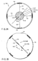
FIGS. 2A and 2B are views showing the wafer
transporting tool shown in FIG. 1, in which FIG. 2A is
a plan view showing the upper surface of the same, and
FIG. 2B is a plan view showing the lower surface of the
same;
FIGS. 3A and 3B are views showing the relationship
between the annular groove and first through holes of
the wafer transporting tool shown in FIGS. 2A and 2B,
in which FIG. 3A is a plan view showing the main part
of the same, and FIG. 3B is a sectional view taken
along the line IIIB - IIIB of FIG. 3A;
FIGS. 4A and 4B are views showing an unload table
in the wafer transporting system of the present
invention, in which FIG. 4A is a plan view showing the
upper surface of the same, and FIG. 4B is a sectional
view taken along the line IVB - IVB of FIG. 4A;
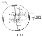
FIG. 5 is a plan view showing the relationship
between a transporting arm and the first through holes
of the wafer transporting tool shown in FIGS. 2A
and 2B;
FIGS. 6A and 6B are views showing an example of a
probe apparatus that employs the transporting system of
the present invention, in which FIG. 6A is a partially
cutaway front view of the same, and FIG. 6B is a plan
view showing the internal arrangement of the same; and
FIGS. 7A and 7B are views showing an example of a
conventional probe apparatus, in which FIG. 7A is a
partially cutaway front view of the same, and FIG. 7B
is a plan view showing the internal arrangement of the
same.
Best Mode for Carrying Out the Invention
The present invention can be applied to various
types of apparatus to process or test an object to be
tested, e.g., a wafer itself, or a plurality of
semiconductor elements or liquid crystal elements on
the wafer.
In the following description, for the sake of more
practical explanation, a probe apparatus which tests
individual semiconductor elements formed on a wafer
will be described. Note that the present invention is
not limited to this probe apparatus.
The present invention will be described with
reference to an embodiment shown in FIGS. 1 to 6B.
A transporting tool to transport a wafer and a
transporting system which transports the wafer,
according to this embodiment, can be suitably used in
the probe apparatus. This probe apparatus can be
basically formed in the same manner as the probe
apparatus shown in FIGS. 7A and 7B. Hence, in the
following description, the transporting tool and
transporting system according to this embodiment will
be described with reference to FIGS. 7A and 7B as well.
As shown in FIG. 1, a main body 11A of a
transporting tool 11 according to this embodiment can
be formed of, e.g., a ceramic flat plate. The
transporting tool 11, with a non-fixed-form wafer
(e.g., in FIG. 1, a cracked wafer from which a portion
indicated by a cracked line is missing) W being placed
on it, is transported between an object-to-be-tested
stage table (to be referred to as a main chuck
hereinafter) 6 and unload table 10 through a
transporting arm (to be referred to as fork
hereinafter) 4. More specifically, the transporting
tool (to be referred to as the wafer transporting tool
hereinafter) 11, with the non-fixed-form wafer (to be
also referred to as the cracked wafer hereinafter) W
being placed on it, is placed on the unload table 10.
The fork 4 move the transporting tool carrying the
cracked wafer W from the unload table 10 onto the main
chuck 6. The main chuck 6 moves in the X, Y, and Z
directions, so that the cracked wafer W on the
transporting tool 11 can be tested. After the test is
ended, the fork 4 transport the transporting tool 11
together with the cracked wafer W from the main chuck 6
to the unload table 10. When the fork 4 transport the
transporting tool 11 with the cracked wafer W being
placed on it, the fork 4 and main chuck 6 are connected
to a vacuum pump through pipes 4C and 6C, respectively.
The fork 4 have at least one first opening 4A in
their upper surface. The first opening 4A can be
connected to an exhaust device (not shown) through an
exhaust channel (not shown). The upper surface of the
main chuck 6 can have a plurality of annular third
grooves 6A to draw the wafer W or transporting tool 11
by vacuum suction. The third grooves 6A are connected
to the exhaust device (not shown) through an exhaust
channel (not shown). Thus, when the transporting tool
11 is placed on the fork 4 or main chuck 6, it is drawn
onto the fork 4 or main chuck 6 by vacuum suction with
a vacuum force from the first opening 4A or third
grooves 6A through the exhaust device.
When the transporting tool 11 is to be drawn onto
the fork 4 or main chuck 6 by vacuum suction, the
suction grooves and through holes formed in the wafer
transporting tool 11 can also be utilized. The suction
grooves and through holes of the wafer transporting
tool 11 will be described with reference to FIGS. 1 to
3B. The transporting tool 11 can be formed of a
ceramic member having a shape larger than that of a
fixed-form wafer (e.g., a complete wafer) W'.
As shown in FIGS. 1, 2A, and 2B, the transporting
tool 11 has a first groove 111 formed at substantially
the center of its first surface 11B, first through
holes 112, and second grooves 113 and second through
holes 114 formed in its second surface 11C. One end of
each first through hole 112 is connected to a second
opening 112A, and the other end thereof is open to the
first groove 111. The second through holes 114 allow
the first and second grooves 111 and 113 to communicate
with each other.
More specifically, the first groove 111 has a
plurality of (six in this embodiment) annular grooves
111A formed concentrically (e.g., with concentric
shapes), and first connection grooves 111B which
connect the annular grooves 111A to each other. The
first connection grooves 111B shown in FIG. 2A connect
the four outer annular grooves. The annular grooves
111A can be formed in such a region that can reliably
draw even a non-fixed-form wafer W having a
comparatively small area due to its missing portion.
The minimum size of the cracked wafer W can be
determined in advance. The size of the cracked wafer W
should be sufficient for covering the annular grooves
111A. As shown in FIG. 2A, the first connection
grooves 111B can extend in the radial direction, and
can be formed equidistantly from each other in the
circumferential direction.
As shown in FIG. 2B, for example, the first
through holes 112 can include eight holes consisting of
pairs. Since the through holes 112 consist of pairs,
evacuation from the through holes 112 can be performed
smoothly.
The four pairs of through holes 112 can be so
arranged as to interpose four intersections, i.e., the
third annular groove 111 counted from the outer side
and the first connection grooves 111B. FIGS. 3A and 3B
show the relationship among the annular grooves 111A,
first connection grooves 111B, and first through holes
112 in enlargement. The positions of the first through
holes 112 correspond to the openings 4A of the fork 4.
For example, as shown in FIG. 5, when the fork 4 are
inserted in the unload table 10, the first through
holes 112 are located in the first openings 4A of the
fork 4, so that the interior of the first groove 111 is
evacuated through the first through holes 112. As
shown in FIGS. 2A and 2B, the first groove 111 can have
second connection grooves 111C which connect the five
outer annular grooves 111A to each other. As shown in
FIG. 2A, the two second connection grooves 111C can
extend in the radial direction at positions where they
do not overlap the first connection grooves 111B. The
second connection grooves 111 can be so formed as to be
located on one straight line.
As shown in FIGS. 2A and 2B, the second grooves
113 can be formed in the other sides of the second
connection grooves 111C. As shown in FIG. 1, the
second grooves 113 can be formed such that, when the
transporting tool 11 is placed on the main chuck 6,
they may intersect the plurality of annular third
grooves 6A formed in the upper surface of the main
chuck 6. The second through holes 114 can be formed at
the intersections of the second connection grooves 111C
and five outer annular grooves 111A. When the upper
surface of the main chuck 6 draws the wafer
transporting tool 11 by vacuum suction, the first
groove 111 can be evacuated through the second grooves
113 and second through holes 114.
As shown in FIG. 2A, four alignment lines 115
which determine the direction of the cracked wafer W
can be formed on the first surface 11B of the wafer
transporting tool 11. The four alignment lines 115
extend from a position slightly outside the annular
grooves 111A to the outer circumference of the wafer
transporting tool 11 radially, and intersect each other
at the center of the annular grooves 111A. One of the
four alignment lines 115 perpendicularly intersects the
center of an orientation flat 116. Accordingly,
the non-fixed-form wafer W is placed on the wafer
transporting tool 11 such that its orientation flat 0
perpendicularly intersects the alignment line 115.
When the non-fixed-form wafer W lacks its orientation
flat 0, it is placed on the wafer transporting tool 11
such that the direction of the scrub line of the
cracked wafer W is aligned with the direction of the
corresponding alignment line 115.
The transporting tool 11 can be made of a ceramic
material into a wafer shape, as described above. The
entire surface of the transporting tool can be covered
with a material having good conductivity, e.g., gold or
a gold alloy. This covering process can be performed
by, e.g., a metal deposition process. The ceramic-made
transporting tool 11 can cope with high-temperature
testing of the non-fixed-form wafer W. When the entire
surface of the wafer transporting tool 11 is covered
with a conductive material, the non-fixed-form wafer W
during testing can be set at ground potential.
The unload table 10 can have a substantially
rectangular shape, as shown in FIG. 4A. Positioning
arrows 101 corresponding to the alignment lines 115 of
the wafer transporting tool 11 can be arranged on the
surface of the unload table 10. The arrows as the
alignment means can be arranged at two positions spaced
apart from each other by 180° in the circumferential
direction. Accordingly, even when a sub chuck 5 (see
FIGS. 7A and 7B) is not used, if the alignment lines
115 of the transporting tool 11 are aligned with the
arrows 101, the direction of the transporting tool 11
and accordingly the direction of the non-fixed-form
wafer W can be aligned by only placing the transporting
tool 11 on the unload table 10. At this time, the
orientation flat 116 of the transporting tool 11
coincides with the position of "FLAT" engraved on the
unload table 10.
As shown in FIG. 4A, a circular disk-like wafer
stage portion 102 is formed at the center of the unload
table 10. As shown in FIG. 4B, the wafer stage portion
102 can have a plurality of wafer supports 102A which
form steps and have different diameters. When a
transporting tool 11 or a fixed-form wafer having a
different outer diameter is placed on the wafer stage
portion 102, the respective wafer supports 102A support
the peripheral portions of the wafer transporting tool
11 and of the fixed-form wafer. An arm entering
portion 102B is formed at the center of the wafer stage
portion 102 in the back-and-forth direction, as
indicated by an alternate long and short dashed line in
FIGS. 4A and 4B. As shown in FIGS. 4A and 4B, the fork
4 enter and retreat from the arm entering portion 102B.
The bottom surface of the arm entering portion 102B is
lower than the lowest wafer support 102A. In FIG. 4A,
the wafer transporting tool 11 is supported by the
wafer support 102A indicated by hatched lines.
As shown in FIG. 6A, the wafer transporting system
of this embodiment can have the unload table 10 which
can move forward and backward in a loader chamber 1,
the fork 4 which transport the transporting tool 11 and
non-fixed-form wafer W placed inside the unload table
10, and the main chuck 606 which places thereon the
transporting tool 11 and cracked wafer W transported
from the fork 4. The main chuck 6 draws and holds the
transporting tool 11 and cracked wafer W simultaneously
by vacuum suction.
A case will be described wherein the cracked wafer
W is to be transported by using the wafer transporting
system described above. First, the unload table 10 is
pulled out from the front surface of the loader chamber
1. The wafer transporting tool 11 is placed on the
wafer supports 102A of the wafer stage portion 102 of
the unload table 10. At this time, the alignment lines
115 of the wafer transporting tool 11 are aligned with
the arrows 101 of the wafer stage portion 102. The
cracked wafer W is placed on the wafer transporting
tool 11. At this time, the orientation flat 0 of the
cracked wafer W is set to perpendicularly intersect
the corresponding alignment line 115 of the wafer
transporting tool 11. The scrub line of the cracked
wafer W is aligned with the direction of the corresponding
alignment line 115. Thus, the cracked wafer W
and wafer transporting tool 11 are prealigned. After
this, the unload table 10 is stored in the loader
chamber.
Subsequently, the probe apparatus is driven
through a control device. The fork 4 enter the arm
entering portion 102B of the unload table 10, and move
upward slightly, as shown in FIGS. 4A and 4B. The
wafer transporting tool 11 is placed on the fork 4. In
this state, the openings 4A of the fork 4 coincide with
the first through holes 112 of the wafer transporting
tool 11, as shown in, e.g., FIG. 5. The alignment
lines 115 are arranged with a shift of 90° from each
other in the circumferential direction. Hence, even
when the alignment lines 115 are prealigned with a
shift of 90° (or 180°, or 270°, the openings 4A of the
fork 4 and the first through holes 112 coincide, as
indicated by an alternate long and short dashed line in
FIG. 5. Successively, the exhaust device is driven
under the control of the control device. The interior
of the first groove 111 is evacuated through the
openings 4A of the fork 4 and the first through holes
112, so that the cracked wafer W and wafer transporting
tool 11 are drawn by suction and fixed on the fork 4.
After the cracked wafer W is drawn by vacuum suction
onto the fork 4, the fork 4 move backward from the
unload table 10. As shown in FIG. 6B, the fork 4
change their direction by 90°, and enter the prober
chamber 2. At this time, the main chuck 6 in the
prober chamber 2 is preferably ready to receive the
cracked wafer W.
After the fork 4 move forward onto the main chuck
6, elevating pins (not shown) of the main chuck 6 move
upward, and simultaneously evacuation of the fork 4 is
stopped. After the elevating pins lift the wafer
transporting tool 11 off the fork 4, the fork 4 move
backward from the prober chamber 2. As the elevating
pins retract into the main chuck 6, the wafer
transporting tool 11 is placed on the main chuck 6.
The second grooves 113 of the transporting tool 11
intersect the third grooves 6A of the main chuck 6.
The control device actuates the exhaust device of
the main chuck 6, thus evacuating the third grooves
6A. The interior of the first groove 111 is
pressure-reduced through the second through holes 114
of the transporting tool 11, and the cracked wafer W
and wafer transporting tool 11 are drawn by suction and
fixed on the main chuck 6.
After that, the main chuck 6 moves to the probe
center, and an alignment mechanism 7 is actuated. An
alignment bridge 7C moves forward to the probe center.
An upper CCD camera 7B photographs the image of the
cracked wafer W, automatically recognizes the state of
arrays of the semiconductor elements in the cracked
wafer W, and grasps the test target of the semiconductor
elements. The main chuck 6 moves in the X
and Y directions to cause the electrodes of the
respective semiconductor elements inside the cracked
wafer W to come into contact with the corresponding
electrodes of the probe card, so that the electrical
characteristics of the semiconductor elements are
tested sequentially.
When the test for the cracked wafer W is ended,
the main chuck 6 moves to a transfer position for the
cracked wafer W. The exhaust device of the main chuck
6 stops, and the elevating pins move upward to lift the
wafer transporting tool 11 off the main chuck 6. The
fork 4 move forward to a space between the main chuck 6
and the lifted wafer transporting tool 11. The exhaust
device of the fork 4 is driven, and the elevating pins
move downward. The fork 4 receive the cracked wafer W
together with the wafer transporting tool 11, and move
along a path opposite to the path for test start, to
return the cracked wafer W together with the wafer
transporting tool 11 to the unload table 10. Thus, the
series of tests is ended.
As has been described above, according to this
embodiment, the transporting tool 11 is placed on the
unload table 10, and the cracked wafer W is placed on
the transporting tool 11. Then, the transporting tool
11 together with the cracked wafer W inside the unload
table 10 can be automatically transported to the main
chuck through the fork 4 and main chuck 6.
According to this embodiment, after the cracked
wafer W is tested, the fork 4 can return the wafer
transporting tool 11 and cracked wafer W from the main
chuck 6 to the unload table 10 automatically.
According to this embodiment, unlike in the
conventional case, the cracked wafer W need not be
placed on the main chuck 6 manually by opening the
prober chamber 2. The cracked wafer W need not be
recovered from the main chuck 6 manually, so that
safety in the test can be ensured.
According to this embodiment, the first groove 111
can have the six concentric annular grooves 111A and
the first connection grooves 111B which connect the
annular grooves 111A. Hence, when transporting the
wafer transporting arm 11 and cracked wafer W through
the fork 4, all the annular grooves 111A and first
connection grooves 111B can be evacuated reliably by
only evacuating them through the fork 4 and first
through holes 112, so that the wafer transporting tool
11 and cracked wafer W can be drawn by suction and
fixed on the fork 4 reliably.
According to this embodiment, the first groove 111
has the second connection grooves 111C which connect
the second through holes 114 to each other. When
transporting the wafer transporting arm 11 and cracked
wafer W through the main chuck 6, all the annular
grooves 111A and first and second connection grooves
111B can be evacuated reliably by only evacuating the
second through holes 114 through the main chuck 6, so
that both the wafer transporting tool 11 and the
cracked wafer W can be drawn by suction and fixed on
the main chuck 6 reliably.
According to this embodiment, the alignment lines
115 which determine the direction of the cracked wafer
W are formed on the surface of the transporting tool
11, and the arrows 101 corresponding to the alignment
lines 115 are formed on the surface of the unload table
10. When placing the wafer transporting tool 11 and
cracked wafer W on the unload table 10, they can be
prealigned.
According to this embodiment, even a non-fixed-form
wafer such as a cracked wafer can be automatically
transported between the wafer storing table and main
chuck (test stage) by only storing it in the wafer
storing table.
According to this embodiment, a transporting tool
to transport a wafer, and transporting system, which
can test a non-fixed-form wafer reliably and safely,
can be provided.
Additional advantages and modifications will
readily occur to those skilled in the art. Therefore,
the invention in its broader aspects is not limited to
the specific details and representative embodiments
shown and described herein.
Accordingly, various modifications may be made
without departing from the spirit or scope of the
general inventive concept as defined by the appended
claims and their equivalents.