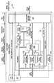
FIELD OF THE INVENTION
The field of this invention is emulation hardware
particularly for highly integrated digital signal processing
systems, and the invention relates to a memory access address
comparator.
BACKGROUND OF THE INVENTION
Advanced wafer lithography and surface-mount packaging
technology are integrating increasingly complex functions at
both the silicon and printed circuit board level of electronic
design. Diminished physical access to circuits for test and
emulation is an unfortunate consequence of denser designs and
shrinking interconnect pitch. Designed-in testability is needed
so the finished product is both controllable and observable
during test and debug. Any manufacturing defect is preferably
detectable during final test before a product is shipped. This
basic necessity is difficult to achieve for complex designs
without taking testability into account in the logic design
phase so automatic test equipment can test the product.
In addition to testing for functionality and for
manufacturing defects, application software development requires
a similar level of simulation, observability and controllability
in the system or sub-system design phase. The emulation phase
of design should ensure that a system of one or more ICs
(integrated circuits) functions correctly in the end equipment
or application when linked with the system software. With the
increasing use of ICs in the automotive industry,
telecommunications, defense systems, and life support systems,
thorough testing and extensive real-time debug becomes a
critical need.
Functional testing, where the designer generates test
vectors to ensure conformance to specification, still remains a
widely used test methodology. For very large systems this
method proves inadequate in providing a high level of detectable
fault coverage. Automatically generated test patterns are
desirable for full testability, and controllability and
observability. These are key goals that span the full hierarchy
of test from the system level to the transistor level.
Another problem in large designs is the long time and
substantial expense involved in design for test. It would be
desirable to have testability circuitry, system and methods that
are consistent with a concept of design-for-reusability. In this
way, subsequent devices and systems can have a low marginal
design cost for testability, simulation and emulation by reusing
the testability, simulation and emulation circuitry, systems and
methods that are implemented in an initial device. Without a
proactive testability, simulation and emulation plan, a large
amount of subsequent design time would be expended on test
pattern creation and upgrading.
Even if a significant investment were made to design a
module to be reusable and to fully create and grade its test
patterns, subsequent use of a module may bury it in application
specific logic. This would make its access difficult or
impossible. Consequently, it is desirable to avoid this
pitfall.
The advances of IC design are accompanied by decreased
internal visibility and control, reduced fault coverage and
reduced ability to toggle states, more test development and
verification problems, increased complexity of design simulation
and continually increasing cost of CAD (computer aided design)
tools. In the board design the side effects include decreased
register visibility and control, complicated debug and
simulation in design verification, loss of conventional
emulation due to loss of physical access by packaging many
circuits in one package, increased routing complexity on the
board, increased costs of design tools, mixed-mode packaging,
and design for produceability. In application development, some
side effects are decreased visibility of states, high speed
emulation difficulties, scaled time simulation, increased
debugging complexity, and increased costs of emulators.
Production side effects involve decreased visibility and
control, complications in test vectors and models, increased
test complexity, mixed-mode packaging, continually increasing
costs of automatic test equipment and tighter tolerances.
Emulation technology utilizing scan based emulation and
multiprocessing debug was introduced more than 10 years ago. In
1988, the change from conventional in circuit emulation to scan
based emulation was motivated by design cycle time pressures and
newly available space for on-chip emulation. Design cycle time
pressure was created by three factors. Higher integration
levels, such as increased use of on-chip memory, demand more
design time. Increasing clock rates mean that emulation support
logic causes increased electrical intrusiveness. More
sophisticated packaging causes emulator connectivity issues.
Today these same factors, with new twists, are challenging the
ability of a scan based emulator to deliver the system debug
facilities needed by today's complex, higher clock rate, highly
integrated designs. The resulting systems are smaller, faster,
and cheaper. They have higher performance and footprints that
are increasingly dense. Each of these positive system trends
adversely affects the observation of system activity, the key
enabler for rapid system development. The effect is called
"vanishing visibility."
Figure 1 illustrates the trend in visibility and control
over time and greater system integration. Application
developers prefer the optimum visibility level illustrated in
Figure 1. This optimum visibility level provides visibility and
control of all relevant system activity. The steady progression
of integration levels and increases in clock rates steadily
decrease the actual visibility and control available over time.
These forces create a visibility and control gap, the difference
between the optimum visibility and control level and the actual
level available. Over time, this gap will widen. Application
development tool vendors are striving to minimize the gap growth
rate. Development tools software and associated hardware
components must do more with less resources and in different
ways. Tackling this ease of use challenge is amplified by these
forces.
With today's highly integrated System-On-a-Chip (SOC)
technology, the visibility and control gap has widened
dramatically over time. Traditional debug options such as logic
analyzers and partitioned prototype systems are unable to keep
pace with the integration levels and ever increasing clock rates
of today's systems. As integration levels increase, system
buses connecting numerous subsystem components move on chip,
denying traditional logic analyzers access to these buses. With
limited or no significant bus visibility, tools like logic
analyzers cannot be used to view system activity or provide the
trigger mechanisms needed to control the system under
development. A loss of control accompanies this loss in
visibility, as it is difficult to control things that are not
accessible.
To combat this trend, system designers have worked to keep
these buses exposed. Thus the system components were built in a
way that enabled the construction of prototyping systems with
exposed buses. This approach is also under siege from the
ever-increasing march of system clock rates. As the central
processing unit (CPU) clock rates increase, chip to chip
interface speeds are not keeping pace. Developers find that a
partitioned system's performance does not keep pace with its
integrated counterpart, due to interface wait states added to
compensate for lagging chip to chip communication rates. At
some point, this performance degradation reaches intolerable
levels and the partitioned prototype system is no longer a
viable debug option. In the current era production devices must
serve as the platform for application development.
Increasing CPU clock rates are also limiting availability
of other simple visibility mechanisms. Since the CPU clock
rates can exceed the maximum I/O state rates, visibility ports
exporting information in native form can no longer keep up with
the CPU. On-chip subsystems are also operated at clock rates
that are slower than the CPU clock rate. This approach may be
used to simplify system design and reduce power consumption.
These developments mean simple visibility ports can no longer be
counted on to deliver a clear view of CPU activity. As
visibility and control diminish, the development tools used to
develop the application become less productive. The tools also
appear harder to use due to the increasing tool complexity
required to maintain visibility and control. The visibility,
control, and ease of use issues created by systems-on-a-chip
tend to lengthen product development cycles.
Even as the integration trends present developers with a
tough debug environment, they also present hope that new
approaches to debug problems will emerge. The increased
densities and clock rates that create development cycle time
pressures also create opportunities to solve them. On-chip,
debug facilities are more affordable than ever before. As high
speed, high performance chips are increasingly dominated by very
large memory structures, the system cost associated with the
random logic accompanying the CPU and memory subsystems is
dropping as a percentage of total system cost. The incremental
cost of several thousand gates is at an all time low. Circuits
of this size may in some cases be tucked into a corner of
today's chip designs. The incremental cost per pin in today's
high density packages has also dropped. This makes it easy to
allocate more pins for debug. The combination of affordable
gates and pins enables the deployment of new, on-chip emulation
facilities needed to address the challenges created by
systems-on-a-chip.
When production devices also serve as the application debug
platform, they must provide sufficient debug capabilities to
support time to market objectives. Since the debugging
requirements vary with different applications, it is highly
desirable to be able to adjust the on-chip debug facilities to
balance time to market and cost needs. Since these on-chip
capabilities affect the chip's recurring cost, the scalability
of any solution is of primary importance. "Pay only for what
you need" should be the guiding principle for on-chip tools
deployment. In this new paradigm, the system architect may also
specify the on-chip debug facilities along with the remainder of
functionality, balancing chip cost constraints and the debug
needs of the product development team.
Figure 2 illustrates an emulator system 100 including four
emulator components. These four components are: a debugger
application program 110; a host computer 120; an emulation
controller 130; and on-chip debug facilities 140. Figure 2
illustrates the connections of these components. Host computer
120 is connected to an emulation controller 130 external to host
120. Emulation controller 130 is also connected to target
system 140. The user preferably controls the target application
on target system 140 through debugger application program 110.
Host computer 120 is generally a personal computer. Host
computer 120 provides access the debug capabilities through
emulator controller 130. Debugger application program 110
presents the debug capabilities in a user-friendly form via host
computer 120. The debug resources are allocated by debug
application program 110 on an as needed basis, relieving the
user of this burden. Source level debug utilizes the debug
resources, hiding their complexity from the user. Debugger
application program 110 together with the on-chip trace and
triggering facilities provide a means to select, record, and
display chip activity of interest. Trace displays are
automatically correlated to the source code that generated the
trace log. The emulator provides both the debug control and
trace recording function.
The debug facilities are preferably programmed using
standard emulator debug accesses through a JTAG or similar
serial debug interface. Since pins are at a premium, the
preferred embodiment of the invention provides for the sharing
of the debug pin pool by trace, trigger, and other debug
functions with a small increment in silicon cost. Fixed pin
formats may also be supported. When the pin sharing option is
deployed, the debug pin utilization is determined at the
beginning of each debug session before target system 140 is
directed to run the application program. This maximizes the
trace export bandwidth. Trace bandwidth is maximized by
allocating the maximum number of pins to trace.
The debug capability and building blocks within a system
may vary. Debugger application program 100 therefore
establishes the configuration at runtime. This approach
requires the hardware blocks to meet a set of constraints
dealing with configuration and register organization. Other
components provide a hardware search capability designed to
locate the blocks and other peripherals in the system memory
map. Debugger application program 110 uses a search facility to
locate the resources. The address where the modules are located
and a type ID uniquely identifies each block found. Once the
IDs are found, a design database may be used to ascertain the
exact configuration and all system inputs and outputs.
Host computer 120 generally includes at least 64 Mbytes of
memory and is capable of running Windows 95, SR-2, Windows NT,
or later versions of Windows. Host computer 120 must support
one of the communications interfaces required by the emulator.
These may include: Ethernet 10T and 100T, TCP/IP protocol;
Universal Serial Bus (USB); Firewire IEEE 1394; and parallel
port such as SPP, EPP and ECP.
Host computer 120 plays a major role in determining the
real-time data exchange bandwidth. First, the host to emulator
communication plays a major role in defining the maximum
sustained real-time data exchange bandwidth because emulator
controller 130 must empty its receive real-time data exchange
buffers as fast as they are filled. Secondly, host computer 120
originating or receiving the real-time data exchange data must
have sufficient processing capacity or disc bandwidth to sustain
the preparation and transmission or processing and storing of
the received real-time data exchange data. A state of the art
personal computer with a Firewire communication channel (IEEE
1394) is preferred to obtain the highest real-time data exchange
bandwidth. This bandwidth can be as much as ten times greater
performance than other communication options.
Emulation controller 130 provides a bridge between host
computer 120 and target system 140. Emulation controller 130
handles all debug information passed between debugger
application program 110 running on host computer 120 and a
target application executing on target system 140. A presently
preferred minimum emulator configuration supports all of the
following capabilities: real-time emulation; real-time data
exchange; trace; and advanced analysis.
Emulation controller 130 preferably accesses real-time
emulation capabilities such as execution control, memory, and
register access via a 3, 4, or 5 bit scan based interface.
Real-time data exchange capabilities can be accessed by scan or
by using three higher bandwidth real-time data exchange formats
that use direct target to emulator connections other than scan.
The input and output triggers allow other system components to
signal the chip with debug events and vice-versa. Bit I/O
allows the emulator to stimulate or monitor system inputs and
outputs. Bit I/O can be used to support factory test and other
low bandwidth, non-time-critical emulator/target operations.
Extended operating modes are used to specify device test and
emulation operating modes. Emulator controller 130 is
partitioned into communication and emulation sections. The
communication section supports host communication links while
the emulation section interfaces to the target, managing target
debug functions and the device debug port. Emulation controller
130 communicates with host computer 120 using one of industry
standard communication links outlined earlier herein. The host
to emulator connection is established with off the shelf cabling
technology. Host to emulator separation is governed by the
standards applied to the interface used.
Emulation controller 130 communicates with the target
system 140 through a target cable or cables. Debug, trace,
triggers, and real-time data exchange capabilities share the
target cable, and in some cases, the same device pins. More
than one target cable may be required when the target system 140
deploys a trace width that cannot be accommodated in a single
cable. All trace, real-time data exchange, and debug
communication occurs over this link. Emulator controller 130
preferably allows for a target to emulator separation of at
least two feet. This emulation technology is capable of test
clock rates up to 50 MHZ and trace clock rates from 200 to 300
MHZ, or higher. Even though the emulator design uses techniques
that should relax target system 140 constraints, signaling
between emulator controller 130 and target system 140 at these
rates requires design diligence. This emulation technology may
impose restrictions on the placement of chip debug pins, board
layout, and requires precise pin timings. On-chip pin macros
are provided to assist in meeting timing constraints.
The on-chip debug facilities offer the developer a rich set
of development capability in a two tiered, scalable approach.
The first tier delivers functionality utilizing the real-time
emulation capability built into a CPU's mega-modules. This
real-time emulation capability has fixed functionality and is
permanently part of the CPU while the high performance real-time
data exchange, advanced analysis, and trace functions are added
outside of the core in most cases. The capabilities are
individually selected for addition to a chip. The addition of
emulation peripherals to the system design creates the second
tier functionality. A cost-effective library of emulation
peripherals contains the building blocks to create systems and
permits the construction of advanced analysis, high performance
real-time data exchange, and trace capabilities. In the
preferred embodiment five standard debug configurations are
offered, although custom configurations are also supported. The
specific configurations are covered later herein.
SUMMARY OF THE INVENTION
This invention is an emulation comparator that can operate
as 2 individual comparators each of them comparing the processor
memory access address (PMAA) and processor memory access data
(PMAD) values issued by a processor against reference values
stored in registers. Alternatively, it can operate as a single
device that compares the memory access address against 2 sets of
reference values forming a double bounded range. The data
contents of the memory access may optionally be used as an extra
qualifier to the address comparison.
The specific resources required for the implementation of
the comparator can vary greatly depending on the requirements
and constraints of a given implementation. In the example
described in this application, the range comparator including 2
single reference address comparators and corresponding data
comparator requires 13 user-visible registers in addition to the
2 address and 2 data compare logic functions.
Each of the 2 comparators can produce independent or
dependent results based on selection made via the control
register. The result of the 2 data comparators can be used as a
qualifier to the associated address comparator or it can be
ignored depending on the control register configuration.
The processor memory access addresses could be of multiple
sizes depending on the processor architecture, such as a byte,
half-word, word, double word. The comparator in the
implementation described here can compare a reference against
memory accesses of multiple sizes.
Aside from the data compare qualification the comparator
can generate a match based on one of six address comparison
criteria. The processor memory access address could be equal to
the reference, not equal to the reference, greater than the
reference, greater than or equal to the reference, less than the
reference or less than or equal to the reference.
This invention enables full or partial overlap criteria.
These are embodied in 2 modes when seeking an equality match. In
the first mode, a match occurs only if the processor memory
access overlaps all of the bytes in the reference. In the
second mode, a match occurs if at least one byte of the
processor memory access overlaps the reference.
The data comparator used in the example described in this
application is an identity equality comparator. The data
comparator produces a match only if all of the bits in the data
that match the corresponding bits in the reference qualified by
the overlap criteria are equal. The data comparator includes a
reference mask value. For the case of the 64 bit memory data
bus of this example, two 32-bit registers are required for each
of the 2 data comparators. The mask allows the customization of
the data bits that are required to match. Thus not necessarily
requiring a match in all of the bits.
The comparator can be programmed via an interface to the
memory map of the processor. This application calls this
interface the configuration bus (cfgb).
The comparator capabilities can be exploited as a tool to
be used by a hardware debug system that will take the comparator
result as an input and will provide a wide range of responses
depending on the configuration of the debug system.
BRIEF DESCRIPTION OF THE DRAWINGS
These and other aspects of this invention are illustrated
in the drawings, in which:
DETAILED DESCRIPTION OF PREFERRED EMBODIMENTS
The ability to detect processor memory access to specific
locations in memory is necessary to help processor code
developers in troubleshooting software problems. The comparator
of this invention is a powerful tool with several features and
good flexibility that supports the software debugging effort.
Other potential applications not related to debugging could
include detection of processor memory access for triggering of
system event interactions or changes in processor operation
context.
The comparator of this invention provides the ability to
detect the occurrence or absence of a processor memory access to
an specific memory address or ranges of addresses that can be
additionally qualified with the data involved in the processor
memory access. Having the comparator integrated within a
hardware debugging system enhances the capability of the system
for detecting and resolving problems in the code being executed
by the processor.
The comparator of this invention enhances the power and
increases the flexibility in the detection of software problems
when debugging process is based on detection of processor memory
accesses. The capability of using full or partial overlap
detection criteria in the comparator is especially important
when the implementation is done for a processor architecture
that can request accesses to memory locations at any byte
boundary. Without this capability proper detection of processor
memory access events in such an architecture will suffer of
serious limitations and in many cases will not even be possible.
Figure 3 illustrates an example of one on-chip debug
architecture embodying target system 140. The architecture uses
several module classes to create the debug function. One of
these classes is event detectors including bus event detectors
210, auxiliary event detectors 211 and counters/state machines
213. A second class of modules is trigger generators including
trigger builders 220. A third class of modules is data
acquisition including trace collection 230 and formatting. A
fourth class of modules is data export including trace export
240, and real-time data exchange export 241. Trace export 240
is controlled by clock signals from local oscillator 245. Local
oscillator 245 will be described in detail below. A final class
of modules is scan adaptor 250, which interfaces scan
input/output to CPU core 201. Final data formatting and pin
selection occurs in pin manager and pin micros 260.
The size of the debug function and its associated
capabilities for any particular embodiment of a system-on-chip
may be adjusted by either deleting complete functions or
limiting the number of event detectors and trigger builders
deployed. Additionally, the trace function can be incrementally
increased from program counter trace only to program counter and
data trace along with ASIC and CPU generated data. The
real-time data exchange function may also be optionally
deployed. The ability to customize on-chip tools changes the
application development paradigm. Historically, all chip
designs with a given CPU core were limited to a fixed set of
debug capability. Now, an optimized debug capability is
available for each chip design. This paradigm change gives
system architects the tools needed to manage product development
risk at an affordable cost. Note that the same CPU core may be
used with differing peripherals with differing pin outs to
embody differing system-on-chip products. These differing
embodiments may require differing debug and emulation resources.
The modularity of this invention permits each such embodiment to
include only the necessary debug and emulation resources for the
particular system-on-chip application.
The real-time emulation debug infrastructure component is
used to tackle basic debug and instrumentation operations
related to application development. It contains all execution
control and register visibility capabilities and a minimal set
of real-time data exchange and analysis such as breakpoint and
watchpoint capabilities. These debug operations use on-chip
hardware facilities to control the execution of the application
and gain access to registers and memory. Some of the debug
operations which may be supported by real-time emulation are:
setting a software breakpoint and observing the machine state at
that point; single step code advance to observe exact
instruction by instruction decision making; detecting a spurious
write to a known memory location; and viewing and changing
memory and peripheral registers.
Real-time emulation facilities are incorporated into a CPU
mega-module and are woven into the fabric of CPU core 201. This
assures designs using CPU core 201 have sufficient debug
facilities to support debugger application program 110 baseline
debug, instrumentation, and data transfer capabilities. Each
CPU core 201 incorporates a baseline set of emulation
capabilities. These capabilities include but are not limited
to: execution control such as run, single instruction step, halt
and free run; displaying and modifying registers and memory;
breakpoints including software and minimal hardware program
breakpoints; and watchpoints including minimal hardware data
breakpoints.
Figure 4 illustrates comparator 400 including two
individual address comparators that integrate the address
component of the range comparator. Comparator 400 is preferably
a part of bus event detectors 210. The flexible combination of
comparator 400 enables detection of numerous types of bus
events. The first comparator is at the top of Figure 4 and the
second comparator is at the bottom. Each address comparator has
4 main components: a processor memory access sampling mechanism
( multiplexers 411, 412, 421 and 422); configuration resources
(bus select register 402, comparator control registers 403 and
405, address reference registers 404 and 406); a program access
address magnitude comparator (memory address magnitude
comparators 413 and 423); and a memory access compare control
block (415 and 425) .
Figure 4 illustrates four multiplexes 411, 412, 421 and 422
serving as the processor memory access sampling mechanism.
Figure 4 illustrates two program memory access address buses.
Multiplexers 411 and 421 select the desired address bus signal
from among the available data address buses dmem_addr_0 and
dmem_addr_1. Multiplexers 412 and 422 select the corresponding
control bus signals mem_acc_ctl_0 and mem_acc_ctl_1 associated
with the selected data address bus. The user controls the bus
selection to the 2 comparators by writing to the bus select
register 402.
Figure 4 illustrates 5 registers which are part of the
comparator configuration. Bus select register 402, comparator
control registers 403 and 405 and address reference registers
404 and 406 can be accessed like other configurable hardware
resource in the processor via a memory interface called a
configuration bus interface (cfgb). This memory interface
includes configuration interface control 401 which receives a
configuration control signal (cfgb_ctl). Configuration data
(cfgb_data) and a configuration clock (cfgb_clk) are supplied to
bus select register 402, comparator control registers 403 and
405 and address reference registers 404 and 406. Upon receipt
of a register write request and the identity of the register via
cfbg_ctl, configuration interface control 401 selects which
register stores the data on the configuration data bus. The
selected register stores the data on the configuration data bus
upon the next configuration clock signal.
Data stored in bus select register 402 defines via
multiplexers 411, 412, 421 and 422 which input bus is compared
against the respective reference values. Multiplexer 411
selects either the first bus dmem_addr_0 or the second bus
dmem_addr_1 for supply to memory address magnitude comparator
413 and memory address byte alignment map maker (BAMM) 414.
Multiplexer 412 selects either the first control bus
mem_acc_ctl_0 or the second control bus mem_acc_ctl_1 for supply
to memory address magnitude comparator 413 and memory address
byte alignment map maker 414. As described below, the ultimate
match determination could depend upon the data size of the
memory access indicated in the respective control bus signals.
The selection of multiplexers 411 and 412 are controlled by bus
select register 402 via port_select_0 signal. Address reference
register 404 supplies a reference address to memory address
magnitude comparator 413 and memory address byte alignment map
maker 414 for the comparison. Multiplexers 421 and 422
similarly select the address and corresponding control bus for
memory address magnitude comparator 423 and memory address byte
alignment map maker 424 under control of bus select register 402
via port_select_1 signal. Address reference register 406 stores
the reference address for memory address magnitude comparator
423 and memory address byte alignment map maker 424.
Memory address magnitude comparators 413 and 423 perform
the actual comparison between the reference value and the
selected processor memory access address. Memory address
magnitude comparators 413 and 423 each generate an equal signal
(EQ) if the processor memory access address equals the reference
address, a greater than signal (GT) if the processor memory
access address is greater than the reference address or a less
than signal (LT) if the processor memory access address is less
than the reference address. Memory address magnitude
comparators 413 and 423 also generate respective offset signals
offset_0 and offset_1. These offset signals are supplied to the
corresponding memory address byte alignment map maker 414 or
424. Memory address magnitude comparator 413 and memory address
byte alignment map maker 414 receive a configuration and control
signal config_&_control_0 from comparator control register 403.
Memory address magnitude comparator 423 and memory address byte
alignment map maker 424 receive a similar configuration and
control signal config_&_control_1 from comparator control
register 405.
Offset signals offset_0 and offset_1 describe the offset in
bytes between the processor memory access address and the
reference address. Respective memory address byte alignment map
makers 414 and 424 generate two signals. The first is called
the reference byte alignment map (ref_bam). The second is
called the memory access byte alignment map (macc_bam). These
signals are fundamental to providing detection of full or
partial overlap between the reference address and the program
memory access address.
Outputs GT, LT, EQ from the memory address magnitude
comparators 413 and 423 and the reference byte alignment map
(ref_bam) and memory access byte alignment map (macc_bam) from
the memory address byte alignment map makers 414 and 424 are
supplied to respective memory access compare control blocks 415
and 425. The memory access byte alignment map signal and the
memory access byte alignment map from the memory address byte
alignment memory makers 414 and 424 are supplied to respective
memory access compare control blocks 415 and 425. Memory access
compare control blocks 415 and 425 generate corresponding
mem_access_event outputs depending on these input signals, the
data comparator qualification from respective OR gates 416 and
426 and the configuration information defined in comparator
control registers 403 and 405. Memory access magnitude
comparators 415 and 425 take the 3 result signals (GT, LT, EQ)
from corresponding memory address magnitude comparators 414 and
424 and expand them into six comparison mode selections. These
are: greater than; less than; equal to; not equal to; less than
or equal to; and greater than or equal to. At the same time the
byte alignment map signals ref_bam and macc_bam are compared
based on the configuration signal from the corresponding
comparison control register 403 or 405 to produce the overlap
match result. Each of the two comparators can be programmed in
one of the 6 comparison modes and using the detection criteria
of that mode with the overlap match result it generates a
partial comparator detection event. Memory access comparison
control block 415 supplies local_event_0 signal to memory access
comparison control block 425. Memory access comparison control
block 425 supplies local_event_1 signal to memory access
comparison control block 415.
Each memory access comparison control block 415 and 425
receives 4 entry lookup table from the corresponding comparator
control register 403 and 405 via respective signals
look_up_table_0 and look_up_table_1. The table look up signals
enable the final outputs mem_access_event_0 and
mem_access_event_1 to depend upon the local_event signal from
the other memory access comparison control block. This
dependency enables address range comparisons with each
comparator testing one for the limit values. Either or both
memory access comparison control blocks 415 and 425 may be
disabled when the central processing unit stall signal
(cpu_stall) is active depending upon the configuration data
stored in respective comparator control registers 403 and 405.
There are several possibilities where a user would be
interested in a memory access not exactly equal to the reference
address. Depending upon the respective data size of the
reference address and the bus address, a bus access having a
different address may touch the reference address. For example,
a word or half word write may overwrite a byte of data without
having the exact address of the data byte. Typically the user
is merely interested in whether the tracked memory access
touches the reference and not interested in the exact data size
and bus address combination. The rule for determining whether a
compare operation is successful can be simply stated as "If any
of the bytes of interest are touched, then the compare is
successful." Such a match depends upon on both the address bus
value and the data size.
The reference address is viewed a series of bytes aligned
to a 32-bit address boundary and populated based on the byte
address of the reference address and the size associated with
the reference address. The size associated with the reference
address can be 1 byte (byte), 2 bytes (half-word), or 4 bytes
(full-word). The bus address is represented in the same
fashion. A comparator match is declared when any of the
following conditions evaluate true. A bus address referencing
any byte of the reference address causes an equals match when
the equals comparison is enabled. A bus address referencing any
byte with a higher address than the highest byte specified by
the reference address causes a greater than match when the
greater than comparison is specified. A bus address referencing
any byte with a lower address than the lowest byte specified by
the reference address creates a less than match when the less
than comparison is specified. Note that all three conditions
can create a match simultaneously. For example, a full word
memory access overlapping a reference address specified as a
byte creates this condition. This allows any size access
touching above, below, or on a specified set of bytes can be
declared a match.
Table 1 shows the five cases for a non-aligned bus
comparison for a memory system supporting full-word, half-word
and byte accesses beginning at any byte addressable boundary.
The three cases in the center of Table 1 are conditional upon
the size of the reference address and bus address. The other
two cases allow a complete comparison without address size
information.
| 32-bit Addresses |
| Reference Address+1 | Reference Address+1 | Reference Address | Reference Address-1 | Reference Address-1 |
| Bus Add > |
| | Bus Add = |
| | | Bus Add = |
| | | | Bus Add = |
| | | | | Bus Add < |
Accesses are divided into a series of 7 byte enables
created from bus address[1:0] and size[1:0] data. These 7 bytes
enables allow the specification of a full word access starting
at any of the byte addresses associated with a 32-bit word
define the position of the bytes affected by the access. Note
that the emulation software should ensure that the memory access
size is greater than or equal to the reference size. Memory
access compare control blocks 415 and 425 receive the GT, LT, EQ
outputs from respective memory address magnitude comparators 413
and 423 and the reference byte alignment map (ref_bam) and
memory access byte alignment map (macc_bam) from respective
memory address byte alignment map makers 414 and 424 and then
form the requested address comparison based upon the respective
bus and reference data sizes.
Table X shows an example coding for the qualification
signals config_&_control_0 and look_up_table_0 stored in
comparator control register 403. Config_&_control_1 and
look_up_table_1 stored in
comparator control register 413 are
similarly coded.
| Bit (s) | Name |
| 11 | EXACT |
| 10:9 | REF |
| 8 | EXE |
| 7 | STALL |
| 6 | ETYPE |
| 5 | Reserved |
| 4 | R/W |
| 3:0 | ACCESS |
The EXACT bit (bit 11) defines the exactness of the address
comparison. If EXACT = 0, then a match occurs for any byte
touching the reference address. If EXACT = 1, then a match
occurs only for an exact address match.
The REF bits (bits 10 and 9) define the size of the address
and data reference values. This is shown in Table X+1.
| REF[10:9] | Reference Size |
| 00 | Byte |
| 01 | Half Word |
| 10 | Word |
| 11 | Double Word |
The EXE bit (bit 8) determines qualification program
counter events. If EXE = 1, the qualification of all program
counter bus events with the execution of a single instruction
from the despatch unit is permitted. If EXE = 0, then
qualification of program counter bus events with single
instruction dispatches is masked. This masking permits a simple
function range based only on addresses (as long as we have STALL
set). This is useful only for program counter address ranges.
The STALL bit (bit 7) controls whether stalls can qualify
as bus events. If STALL = 1, then qualification of bus events
with active pipeline cycles is masked. This permits a block
range event as a level as long as the EXE bit is 0. This is
useful only for program counter address ranges. If STALL = 0,
then stalls in the data access and program counter access are
permitted to qualify bus events.
The ETYPE bit (bit 6) controls detection of emulation
memory accesses. When ETYPE = 0, emulation access cycles are
not detected.
The R/W bit (bit 4) determines whether the match is made
for a read operation or a write operation. If R/W = 1, then the
comparator detects on a read operation. If R/W = 0, then the
comparator detects on a write operation.
The QLU field (bits 3:0) defines the bus event
qualification necessary for data size. Table X+2 shows the
coding of these bits.
| Bits [3:0] | Access Size Detected |
| 0000 | No accesses |
| 0001 | Byte |
| 0010 | Half Word |
| 0011 | Half Word and Byte |
| 0100 | Word |
| 0101 | Word and Byte |
| 0110 | Word and Half Word |
| 0111 | Word, Half Word and Byte |
| 1000 | Double Word |
| 1001 | Double Word and Byte |
| 1010 | Double Word and Half Word |
| 1011 | Double Word, Half Word and Byte |
| 1100 | Double Word and Word |
| 1101 | Double Word, Word and Byte |
| 1110 | Double Word, Word and Half Word |
| 1111 | Double Word, Word, Half Word and Byte |
These bits determine which access size or sizes are of interest
to the bus detection hardware. The lookup table maps a set of
bits to the access size(s) detected.
Figure 5 illustrates a companion data comparator. The
preferred embodiment uses two data comparators 500, one
supplying each memory access comparison control block 415 and
425 via respective OR gates 416 and 426. In many
implementations it is acceptable to use a only single data
comparator 500 shared by both address comparators. This would
cost some reduction in flexibility.
The preferred embodiment of data comparator 500 operates on
a 64-bit data bus and thus requires twice as many resources in
the data path that what will be required for a 32-bit data bus
implementation. Data comparator 500 includes six sections of
logic: configuration resources (401, 402, 403, 404, 505, 506 and
507); sampling logic (510, 511, 512, 513, 514); memory data
identity comparators (521 and 522); a memory access data-byte
address-range overlap detector (530); and a memory access data
compare control (540).
The configuration resources include configuration interface
control 401 and seven registers. Bus select register 402 and
interface control 401 are shared with the address comparator 400
illustrated in Figure 4. Comparator control register 403 and
address reference register 404 are shared with the corresponding
address comparison function. Sixty four bits of comparison data
are stored as two 32-bit words. Data reference register low
(data_reference_reg_1) 505 stores the 32 least significant bits
and data reference register high (data_reference_reg_h) 507
stores the 32 most significant bits. Sixty four bits of mask
data are stored as two 32-bit words. Mask register low
(mask_reg_1) 506 stores the 32 least significant bits and mask
register high (mask_reg_h) 508 stores the 32 most significant
bits. Bit locations in mask resisters 506 and 508 set to 0 are
assumed match and those set to 1 are compared. These registers
can be accessed like other configurable hardware resource in the
processor via a configuration bus and configuration interface
control 401.
The sampling logic defines the selection of the data bus
and associated control and address information related to the
memory access. Multiplexer 511 selects either 32 least
significant bit data bus mem_data_low_0 or mem_data_low_0 for
supply to memory data byte identity comparator low 521.
Multiplexer 512 selects either 32 most significant bit data bus
mem_data_high_0 or mem_data_high_0 for supply to memory data
byte identity comparator low 522. The selections are controlled
by data multiplexer and path control logic 510 responsive to the
port_select signal from bus select register 402 and to the
memory access control signals mem_acc_ctl_0 and mem_acc_ctl_1,
which correspond to respective data buses. The user controls
the bus selection to use for the comparison by writing to the
bus select register 402.
Memory data byte identity comparator low 521 receives 32
least significant bits of reference data from data reference low
register 505, 32 least significant bits of mask data from mask
register low 506 and the selected 32 least significant bits of
memory data from multiplexer 511. Memory data byte identity
comparator high 522 similarly receives 32 most significant bits
of reference data from data reference high register 507, 32
least significant bits of mask data from mask register high 508
and the selected 32 most significant bits of memory data from
multiplexer 512. Memory data byte identity comparators 521 and
522 generate corresponding match signals byte_data_match_0 and
byte_data_match_1. Memory data byte identity comparators 521
and 522 each use the corresponding mask to do identity
comparison on each individual byte of the data bus. Each bus
match signal separately indicates a match for the corresponding
four bytes. This enables operation on multiple sizes
concurrently. Assuming the smallest data size is a byte and all
other sizes are a byte multiple, then data comparator can
provide a match indication for any one of 4 data sizes: byte (8
bits); half-word (16 bits); word (32 bits); and double-word (64
bits).
Memory access data byte address range overlap detector 530
generates information about the relative overlap between the
bytes of the memory-access and the bytes of the reference,
address_byte_overlap. Multiplexer 513 selects one memory access
control signal mem_acc_ctl_0 or mem_acc_ctl_1 under control of
the port_select signal from data multiplexer and path control
logic 510. Multiplexer 514 similarly selects one of the address
buses dmem_addr_0 and dmem_addr_1 under control of the port
select signal. Memory access data byte address range overlap
detector 530 receives the selected memory bus control signals
from multiplexer 513, the selected address bus signal from
multiplexer 514, the address from address reference register 404
and a configuration and control signal from comparator control
register 403. Memory access data byte address range overlap
detector 530 produces eight overlap signals
(address_byte_overlap) calculated similarly to overlap
calculation used in address comparator 400 to generate the byte
alignment map.
Memory access data compare control 540 generates the
data_compare_result_0. Memory access data compare control 540
receives: eight partial data comparison results, four are
byte_data_match_1 from memory data byte identity comparator 521
and four are byte_data_match_h from memory data byte identity
comparator 522; the eight address_byte_overlap signals from
memory access data byte address range overlap detector 530;
control bus information from the memory access (mem_acc_ctl_0
and mem_acc_ctl_1); and the look up table data from comparator
control register 403. Memory access data compare control 540
uses these signals to generate the data match signal
(data_compare_result_0). As described above in, this data match
signal can used to qualify the address comparison.
Table 2 illustrates the manner of duplication of values for
a reference data size less than a double-word.
| Ref Size | B7 | B6 | B5 | B4 | B3 | B2 | B1 | B0 |
| Byte | Value | Value | Value | Value | Value | Value | Value | Value |
| Half Word | Value | Value | Value | Value |
| Word | Value | Value |
| Dbl word | Value |
The columns B0 to B7 correspond to the eight bytes in data
reference register low 505 and data reference register high 507.
Low bytes B0 to B3 are stored in data reference register low 505
and high bytes B4 to B7 are stored in data reference register
high 507. Duplication of data in this fashion together with
appropriate byte strobes will permit any desired match for any
combination of memory access size and reference size. Only the
data bytes references by an access are included in the data
comparison.
The preferred embodiment of this invention includes two
data comparators 500. The first is as illustrated in Figure 5.
The second address comparator is similar except that comparator
control register 403 is replaced with comparator control
register 405, address reference register 404 is replaced with
address reference register 406 and the compare output
data_compare_result_1 is supplied to OR gate 426 rather than OR
gate 416. As a further alternative, two data comparators as
shown in Figure 5 may be employed together to perform a data
range comparison. One data comparator would detect the lower
boundary of the data range and the second data comparator would
detect the upper boundary of the data range. The result of this
data range comparison may be supplied via the data comparator
qualification signals to a selected one of or to both of data
compare qualification OR gates 416 and 426.