EP1428407B1 - Optical switching device for wavelength division multiplex (wdm) telecommunications network - Google Patents
Optical switching device for wavelength division multiplex (wdm) telecommunications network Download PDFInfo
- Publication number
- EP1428407B1 EP1428407B1 EP02796342A EP02796342A EP1428407B1 EP 1428407 B1 EP1428407 B1 EP 1428407B1 EP 02796342 A EP02796342 A EP 02796342A EP 02796342 A EP02796342 A EP 02796342A EP 1428407 B1 EP1428407 B1 EP 1428407B1
- Authority
- EP
- European Patent Office
- Prior art keywords
- mirrors
- input
- array
- arrays
- output
- Prior art date
- Legal status (The legal status is an assumption and is not a legal conclusion. Google has not performed a legal analysis and makes no representation as to the accuracy of the status listed.)
- Expired - Lifetime
Links
- 230000003287 optical effect Effects 0.000 title claims abstract description 50
- 230000005855 radiation Effects 0.000 claims abstract description 45
- 238000003491 array Methods 0.000 claims abstract description 41
- 239000000969 carrier Substances 0.000 claims abstract description 23
- XUIMIQQOPSSXEZ-UHFFFAOYSA-N Silicon Chemical compound [Si] XUIMIQQOPSSXEZ-UHFFFAOYSA-N 0.000 claims description 9
- 229910052710 silicon Inorganic materials 0.000 claims description 9
- 239000010703 silicon Substances 0.000 claims description 9
- 239000000758 substrate Substances 0.000 claims description 8
- 230000008929 regeneration Effects 0.000 description 11
- 238000011069 regeneration method Methods 0.000 description 11
- 238000000926 separation method Methods 0.000 description 8
- 238000010586 diagram Methods 0.000 description 7
- 238000006243 chemical reaction Methods 0.000 description 6
- 239000000470 constituent Substances 0.000 description 4
- 239000000835 fiber Substances 0.000 description 4
- 230000005540 biological transmission Effects 0.000 description 1
- 238000004519 manufacturing process Methods 0.000 description 1
- 238000000034 method Methods 0.000 description 1
- 230000010355 oscillation Effects 0.000 description 1
- 230000001172 regenerating effect Effects 0.000 description 1
- 238000004513 sizing Methods 0.000 description 1
Images


Classifications
-
- G—PHYSICS
- G02—OPTICS
- G02B—OPTICAL ELEMENTS, SYSTEMS OR APPARATUS
- G02B6/00—Light guides; Structural details of arrangements comprising light guides and other optical elements, e.g. couplings
- G02B6/24—Coupling light guides
- G02B6/26—Optical coupling means
- G02B6/35—Optical coupling means having switching means
- G02B6/3564—Mechanical details of the actuation mechanism associated with the moving element or mounting mechanism details
- G02B6/3566—Mechanical details of the actuation mechanism associated with the moving element or mounting mechanism details involving bending a beam, e.g. with cantilever
-
- G—PHYSICS
- G02—OPTICS
- G02B—OPTICAL ELEMENTS, SYSTEMS OR APPARATUS
- G02B6/00—Light guides; Structural details of arrangements comprising light guides and other optical elements, e.g. couplings
- G02B6/24—Coupling light guides
- G02B6/26—Optical coupling means
- G02B6/28—Optical coupling means having data bus means, i.e. plural waveguides interconnected and providing an inherently bidirectional system by mixing and splitting signals
- G02B6/293—Optical coupling means having data bus means, i.e. plural waveguides interconnected and providing an inherently bidirectional system by mixing and splitting signals with wavelength selective means
- G02B6/29304—Optical coupling means having data bus means, i.e. plural waveguides interconnected and providing an inherently bidirectional system by mixing and splitting signals with wavelength selective means operating by diffraction, e.g. grating
- G02B6/29305—Optical coupling means having data bus means, i.e. plural waveguides interconnected and providing an inherently bidirectional system by mixing and splitting signals with wavelength selective means operating by diffraction, e.g. grating as bulk element, i.e. free space arrangement external to a light guide
- G02B6/2931—Diffractive element operating in reflection
-
- G—PHYSICS
- G02—OPTICS
- G02B—OPTICAL ELEMENTS, SYSTEMS OR APPARATUS
- G02B6/00—Light guides; Structural details of arrangements comprising light guides and other optical elements, e.g. couplings
- G02B6/24—Coupling light guides
- G02B6/26—Optical coupling means
- G02B6/28—Optical coupling means having data bus means, i.e. plural waveguides interconnected and providing an inherently bidirectional system by mixing and splitting signals
- G02B6/293—Optical coupling means having data bus means, i.e. plural waveguides interconnected and providing an inherently bidirectional system by mixing and splitting signals with wavelength selective means
- G02B6/29304—Optical coupling means having data bus means, i.e. plural waveguides interconnected and providing an inherently bidirectional system by mixing and splitting signals with wavelength selective means operating by diffraction, e.g. grating
- G02B6/29305—Optical coupling means having data bus means, i.e. plural waveguides interconnected and providing an inherently bidirectional system by mixing and splitting signals with wavelength selective means operating by diffraction, e.g. grating as bulk element, i.e. free space arrangement external to a light guide
- G02B6/29313—Optical coupling means having data bus means, i.e. plural waveguides interconnected and providing an inherently bidirectional system by mixing and splitting signals with wavelength selective means operating by diffraction, e.g. grating as bulk element, i.e. free space arrangement external to a light guide characterised by means for controlling the position or direction of light incident to or leaving the diffractive element, e.g. for varying the wavelength response
-
- H—ELECTRICITY
- H04—ELECTRIC COMMUNICATION TECHNIQUE
- H04Q—SELECTING
- H04Q11/00—Selecting arrangements for multiplex systems
- H04Q11/0001—Selecting arrangements for multiplex systems using optical switching
- H04Q11/0005—Switch and router aspects
-
- G—PHYSICS
- G02—OPTICS
- G02B—OPTICAL ELEMENTS, SYSTEMS OR APPARATUS
- G02B6/00—Light guides; Structural details of arrangements comprising light guides and other optical elements, e.g. couplings
- G02B6/24—Coupling light guides
- G02B6/26—Optical coupling means
- G02B6/35—Optical coupling means having switching means
- G02B6/351—Optical coupling means having switching means involving stationary waveguides with moving interposed optical elements
- G02B6/3512—Optical coupling means having switching means involving stationary waveguides with moving interposed optical elements the optical element being reflective, e.g. mirror
- G02B6/3518—Optical coupling means having switching means involving stationary waveguides with moving interposed optical elements the optical element being reflective, e.g. mirror the reflective optical element being an intrinsic part of a MEMS device, i.e. fabricated together with the MEMS device
-
- G—PHYSICS
- G02—OPTICS
- G02B—OPTICAL ELEMENTS, SYSTEMS OR APPARATUS
- G02B6/00—Light guides; Structural details of arrangements comprising light guides and other optical elements, e.g. couplings
- G02B6/24—Coupling light guides
- G02B6/26—Optical coupling means
- G02B6/35—Optical coupling means having switching means
- G02B6/354—Switching arrangements, i.e. number of input/output ports and interconnection types
- G02B6/3554—3D constellations, i.e. with switching elements and switched beams located in a volume
- G02B6/3556—NxM switch, i.e. regular arrays of switches elements of matrix type constellation
-
- G—PHYSICS
- G02—OPTICS
- G02B—OPTICAL ELEMENTS, SYSTEMS OR APPARATUS
- G02B6/00—Light guides; Structural details of arrangements comprising light guides and other optical elements, e.g. couplings
- G02B6/24—Coupling light guides
- G02B6/26—Optical coupling means
- G02B6/35—Optical coupling means having switching means
- G02B6/354—Switching arrangements, i.e. number of input/output ports and interconnection types
- G02B6/356—Switching arrangements, i.e. number of input/output ports and interconnection types in an optical cross-connect device, e.g. routing and switching aspects of interconnecting different paths propagating different wavelengths to (re)configure the various input and output links
-
- H—ELECTRICITY
- H04—ELECTRIC COMMUNICATION TECHNIQUE
- H04J—MULTIPLEX COMMUNICATION
- H04J14/00—Optical multiplex systems
- H04J14/02—Wavelength-division multiplex systems
-
- H—ELECTRICITY
- H04—ELECTRIC COMMUNICATION TECHNIQUE
- H04Q—SELECTING
- H04Q11/00—Selecting arrangements for multiplex systems
- H04Q11/0001—Selecting arrangements for multiplex systems using optical switching
- H04Q11/0005—Switch and router aspects
- H04Q2011/0007—Construction
- H04Q2011/0016—Construction using wavelength multiplexing or demultiplexing
-
- H—ELECTRICITY
- H04—ELECTRIC COMMUNICATION TECHNIQUE
- H04Q—SELECTING
- H04Q11/00—Selecting arrangements for multiplex systems
- H04Q11/0001—Selecting arrangements for multiplex systems using optical switching
- H04Q11/0005—Switch and router aspects
- H04Q2011/0007—Construction
- H04Q2011/0024—Construction using space switching
-
- H—ELECTRICITY
- H04—ELECTRIC COMMUNICATION TECHNIQUE
- H04Q—SELECTING
- H04Q11/00—Selecting arrangements for multiplex systems
- H04Q11/0001—Selecting arrangements for multiplex systems using optical switching
- H04Q11/0005—Switch and router aspects
- H04Q2011/0007—Construction
- H04Q2011/0026—Construction using free space propagation (e.g. lenses, mirrors)
Definitions
- the present invention relates to an optical switching device for use in a WDM telecommunications network for selectively switching wavelength components (wavelength carriers) of WDM radiation to a selected output. More especially the invention concerns an optical switching device in which the switching is carried out optically using MEMS (Micro Electro Mechanical System) moveable reflectors or mirrors.
- MEMS Micro Electro Mechanical System
- OXCs Optical cross-connects
- One known OXC comprises two arrays of MEMS moveable mirrors that face one another in which the first and second arrays are associated with the input fibres and output fibres respectively.
- Each array comprises a two-dimensional planar array of mirrors in which each mirror of the array is independently controllable and tiltable about two orthogonal axes.
- An input collimator arrangement is provided to direct WDM radiation from each of the input fibres onto a respective mirror of the first array and an output collimator arrangement provided to couple WDM radiation received from each of the mirrors of the second array into a respective output fibre.
- Each mirror of the first array can be tilted such as to selectively direct radiation onto any one of the mirrors of the second array and each mirror in the second plane is appropriately oriented such as to direct the radiation received thereat to the respective output collimator.
- Such an optical switching arrangement is totally flexible in that it is capable of selectively connecting any one of the plurality of input fibres to any one of the plurality of output fibres making the arrangement ideally suited as a fibre switch.
- the need to be able to accurately tilt each mirror of the array individually about two axes makes control complex.
- the design is also complex because of the need for precise alignment about three dimensions (3D).
- the number of inputs that such an OXC is able to selectively connect is constrained by the maximum inclination angle of each of the mirrors and this places a limit on the size of the array.
- Many solutions have been proposed for precisely orienting the mirrors but these often involve the use of high voltage electrostatic driver members making OXC with a large number of inputs/outputs expensive and bulky.
- an optical switching device comprising: a plurality of optical input paths and a plurality of optical output paths; a first array of individually selectably tiltable MEMS mirrors in which each mirror is for receiving optical radiation from a respective input path; and a second array of individually selectably tiltable MEMS mirrors in which each mirror is for deflecting optical radiation incident thereon along a respective output path, and is characterised in that the first and second arrays of mirrors are arranged on a common plane and are selectably tiltable about a single axis and a fixed reflector is arranged above the two arrays of mirrors, wherein in operation optical radiation received along each input path is deflected by its respective mirror of the first array via the fixed reflector to a selected mirror of the second array and there from to its respective output path.
- the switching device is for switching wavelength carriers (components) from a plurality of input DWDM radiation inputs to a selected DWDM output and wherein the mirrors of the first and second arrays are arranged in rows and columns and in which each row is associated a DWDM input and each column associated with a respective wavelength carrier.
- the switching device further comprises means for separating each of the plurality of input DWDM radiation into its respective wavelength carriers and directing each carrier along a respective input path.
- separation means includes a wavelength selective component such as a diffraction grating or AWG to spatially separate the DWDM radiation into its constituent wavelength components (carriers).
- the separating means further includes collimating means for collimating and directing each wavelength carrier along a respective input path.
- the switching device further comprises means for combining radiation from a plurality of output paths to produce a DWDM output.
- the switching device preferably further comprises additional arrays of individually selectably tiltable MEMS mirrors, said mirrors being tiltable about a single axis that is transverse to the axis of the mirrors of the first and second arrays and wherein said additional arrays are for respectively selectively adding radiation to an input path dropping radiation intended for an output path.
- each of the array of mirrors are fabricated on a single silicon substrate.
- FIG. 1 there is shown a block schematic representation of an optical switching arrangement 10 in accordance with the present invention for use in a DWDM (Dense WDM) telecommunications network.
- the switching arrangement 10 has four optical inputs (i/p-1 to i/p-4) and four optical outputs (o/p-1 to o/p-4) for receiving and outputting thereat DWDM radiation 11a to 11d and 12a to 12d.
- the DWDM radiation comprises n wavelength carriers ⁇ 1 to ⁇ n , for example sixteen wavelength carriers.
- the optical switching arrangement 10 is operable to selectively switch the individual wavelength components ⁇ 1 to ⁇ n (wavelength carriers) of DWDM radiation applied to the four inputs i/p-1 to i/p-4 to a selected output i/p-1 to i/p-4.
- the arrangement comprises in order between the inputs and outputs: a wavelength separation unit (de-multiplexer) 14, an optical switching device 13 and a wavelength combiner unit (multiplexer) 15.
- the wavelength separation unit 14 is operable to separate each of the input DWDM radiation 11a to 11d into its constituent wavelength components (carriers/channels) that are then input along respective paths to the switching device 13.
- the wavelength combiner unit 15 is operable to combine the radiation components output from the switching device 13 to produce DWDM radiation 12a to 12d that is output from the switching arrangement.
- the wavelength separation unit 14 is shown in greater detail in Figure 2 .
- a known frequency (wavelength) selective device 16 diffiffraction grating
- Each input DWDM radiation is directed, in the form of a collimated beam, onto the grating in order to separate the chromatic (wavelength) components.
- the beams of radiation at the respective wavelengths are made parallel and collimated by collimators 19 and directed along the paths denoted ⁇ 1 to ⁇ n towards a respective mirror of a MEMS array 18 contained in the switching device 13.
- Each wavelength component of each DWDM input is thus focused on a respective mirror of the MEMS array 18. Again for the sake of clarity only paths for a single input i/p-1 are illustrated in Figure 2 .
- frequency selective components 16 can be placed outside the switching arrangement; in this case fibres dedicated to single wavelength carrier will be supplied to feed the collimators.
- the wavelength combiner unit (multiplexer)15 connected to the output of the switching device is similar to the wavelength separation unit just described with input and output exchanged and is not further described as it is readily realised by those skilled in the art.
- Figure 3 illustrates the functional topology of the optical switching device 13. As can be seen it is a device for re-routing a wavelength from an input set i/p-x @ ⁇ i to an output set o/p-x @ ⁇ i where x is the number of the DWDM input/output and i is the wavelength carrier. The same topology is repeated for each wavelength carrier in the WDM grid (for example 40 channels for ITU-T 100GHz).
- the switching device comprises a 4x4 switch (i.e. having four DWDM inputs and outputs). To realize switching arrangements having more than four inputs it is preferred to build these using a plurality of 4 x 4 switching device in separate switching planes.
- any wavelength component from any DWDM input can be switched to a corresponding channel (i.e. the same carrier wavelength) of the desired output.
- Practical considerations suggest expanding the DWDM network in layers and adding new switching planes with interconnectivity in the plane but not between different planes.
- the basic 'building block' of the switching arrangement of the present invention is the optical switching device 13 that comprises two arrays of moveable mirrors that are rotatable (tiltable) about a single axis.
- An input array of mirrors 18 is provided for the input of the switching device 13 and an output array 23 for the output.
- Each mirror array comprises an m X n array of individually controllable mirrors in which m is the number of DWDM inputs (4 in the example being described) and n the number of wavelength channels within each DWDM input.
- Figure 4 shows diagrammatically an input array 18 of mirrors with ray diagrams represented for a single input i/p-1 for each of the wavelength carriers ⁇ 1 to ⁇ n .
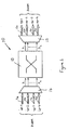
- the mirror arrays are preferably fabricated as silicon MEMS having the mirrors (reflectors) etched on silicon surface by well-tested procedures. Each mirror can be individually deflected (tilted) by an associated driver (not shown).
- a mirror array is shown schematically in Figure 5 (side view) and Figure 6 (top view). These figures show a plurality of parallel flexible silicon strips 20 whose upper surface has been processed to make it reflecting. A respective driver 21 is provided below each strip for controlling deflection of the strip to a desired inclination a about a single axis.
- Figures 5 and 6 are descriptive only of the concept of the mirror array and a practical realization would be readily imaginable to those skilled in the art.
- the mirrors can alternatively be secured to the flexible silicon strip instead of making the strip itself reflecting. This is shown diagrammatically in Figure 7 in which a mirror 22 is mounted on the flexible strip 20.
- a cardan mount arrangement can be used.
- the MEMS mirror arrays 18 and 23 are arranged parallel on a common reference plane and a fixed reflecting plane (ceiling) 24 provided over the assembly.
- the fixed reflecting plane is preferably parallel with the plane on which the input and output mirror arrays are mounted.
- the rays arrive from the input collimator and the rays, denoted o/p-1@ ⁇ 1 to o/p-4@ ⁇ 1 , are directed towards the output collimator.
- the rays indicate that i/p-1 and i/p-2 are connected to o/p-1 and o/p-2 whilst i/p-3 and i/p-4 are respectively cross-connected to o/p-4 and o/p-3.
- the dashed line indicates an alternative connected of i/p-3 to its corresponding output o/p-3.
- the interconnection between input and output is determined by the inclination of the mirrors within the input array 18.
- the switching device 13 further includes a number of ADD inputs ( ⁇ Channels-in) 40 and DROP outputs ( ⁇ Channels-out) 41 for connection to a conversion and regeneration block 31.
- the block 31 is operable for converting the wavelength and regenerating wavelength carriers. Conversion and regeneration devices are known to those skilled in the art and are not further described or shown.
- each ADD input or DROP output should be usable for any desired wavelength carrier.
- a further array of MEMS mirrors is provided within the switching device 13. These arrays of mirrors are similar to the array described above except that the angular movement of the mirrors is about a different axis, preferably about an axis that is orthogonal to that of the axis of the input and output MEMS. Referring to Figure 11 there is shown, (a) a mirror array with a transverse axis of movement and, (b) a mirror array with a normal axis of movement.
- the switching device 13 including the ADD/DROP function for dropping and inserting wavelength carrier within the switching path is shown in Figures 12 (side view) and 13 (plan view). As may be seen in these figures, as compared to the embodiment described above with reference to Figure 8 , the switching device 13 further includes transversal pairs of mirror arrays 35 and 36, 37 and 38 located at the input and output of the switching device.
- the pair of transversal arrays 35 and 36 at the input of the switch are for receiving input radiation from an ADD input and selectively directing it to the input array 18.
- the pair of transversal arrays 37, 38 at the output of the switching device are for selectively directing radiation from the output array 23 to a DROP output 40.
- transversal arrays 25, 36, 37 and 38 The function performed by the transversal arrays 25, 36, 37 and 38 will be more clearly understood with reference to Figure 13 which is a plan view along a direction "A" of Figure 12 .
- the mirrors of the normal arrays 18, 23 have an axis of rotation that runs in a vertical direction as viewed in the figure whilst the transversal arrays 35, 36, 37, 38 have an axis of rotation running in a horizontal direction.
- radiation at the ADD input is focused on the first transversal array 35 by a collimator 42.
- the array 35 reflects this radiation via the reflecting ceiling 24 of the device and there from to a selected mirrors of the transversal array 36 which redirects the radiation into a normal path between the arrays 18 and 23.
- each wavelength carrier can be added or dropped using arrays of mirrors that are moveable about a single axis.
- Figures 12 and 13 are not to scale and illustrate a single wavelength carrier ⁇ 1 being dropped to the output 41 and a single wavelength carrier ⁇ 4 being added via the input 40.
- the intrinsic structure of C and L band commercial transmission systems suggests division of the wavelength carriers into sub-bands to allow greater scalability.
- the dimension of a basic switching arrangement can thus be considered to be 40 wavelength channels (carriers) in accordance with ITU-T 100GHz grids.
- regeneration ports having ten inputs and outputs for each DWDM input is required.
- forty regeneration inputs 40 and outputs 41 are required.
- a single switching arrangement capable of switching 160 channels, that is 40 channels of the first 100GHz grid in band C.
- the arrangement can then be progressively updated to 640 wavelength channels.
- multiple layers can be provided. Routing between layers is preferably avoided, although limited interconnection between the layers is possible via the respective regenerator and converters of each layer. This is shown in a block diagram in Figure 14 in which the constituent components of switching arrangement will be readily identifiable to those skilled in the art.
- Such a layered structure allows realizing, for example, the switching of 1280 wavelength channels (carriers).
- the optical switching device is free of wavelength selective components such as those required in the wavelength separation and combiner units 14 and 15. It is preferable therefore that all such wavelength selective filters or AWGs used to separate/combine the individual wavelength carriers from/to the DWDM radiation are positioned outside of the MEMS optical switching device 13 rather than being a part of this assembly.
- Multiple-fibre optical connectors can be used to connect the optical switching device to external optical circuitry. Input to and output from the switching device can be provided, for example, using individual fibres organized in multiple-fibre optical connectors for each DWDM input/output.
- the processed silicon substrate 45 is then be housed on an inner wall of a housing 50 with the reflecting surface 24 (ceiling) being defined by the facing inner wall of the housing.
- a collimator array 51 for the ADD function On the inner wall of the housing upon which the substrate 45 is mounted there are provided to one side of the substrate, a collimator array 51 for the ADD function and a collimator array 52 for the input.
- a collimator array 53 for the DROP function On the opposite side of the substrate 45 there are provided a collimator array 53 for the DROP function and a collimator array 54 for the output.
- the channels to be added are connected through the first row of collimators of the collimator array 51 and are dedicated to the input channels incoming through the first row of the input collimator array 52.
- the channels dropped through the first row of collimators in the collimator array 54 arrive from the input channels through the first row of the output collimator array. The same correspondence applies to remaining rows of the arrays.
- any wavelength of the N th input/output row can be intercepted by any ADD/DROP collimator of the Nth row.
- Figure 18 shows a graph of the increase ⁇ of angle of inclination ⁇ of the mirrors as a function of height h of the reflecting ceiling above the plane on which the mirror arrays are mounted.
- Figure 19 illustrates the geometry of the optical switching device and indicates the parameters involved in the calculation of the data in Figure 18 .
- ⁇ arctan 2 ⁇ h ⁇ L L ⁇ L + ⁇ L + 4 ⁇ hh in which L is the separation between a mirror of the input array and the corresponding mirror of the output array and ⁇ L is the spacing (pitch) of rows of mirrors in the input and output array.
Landscapes
- Physics & Mathematics (AREA)
- General Physics & Mathematics (AREA)
- Optics & Photonics (AREA)
- Engineering & Computer Science (AREA)
- Computer Networks & Wireless Communication (AREA)
- Use Of Switch Circuits For Exchanges And Methods Of Control Of Multiplex Exchanges (AREA)
- Mechanical Light Control Or Optical Switches (AREA)
- Optical Communication System (AREA)
Abstract
Description
- The present invention relates to an optical switching device for use in a WDM telecommunications network for selectively switching wavelength components (wavelength carriers) of WDM radiation to a selected output. More especially the invention concerns an optical switching device in which the switching is carried out optically using MEMS (Micro Electro Mechanical System) moveable reflectors or mirrors.
- Optical cross-connects (OXCs) are known that are capable of switching WDM optical radiation arriving from a plurality of input fibres to selected output fibres. One known OXC comprises two arrays of MEMS moveable mirrors that face one another in which the first and second arrays are associated with the input fibres and output fibres respectively. Each array comprises a two-dimensional planar array of mirrors in which each mirror of the array is independently controllable and tiltable about two orthogonal axes. An input collimator arrangement is provided to direct WDM radiation from each of the input fibres onto a respective mirror of the first array and an output collimator arrangement provided to couple WDM radiation received from each of the mirrors of the second array into a respective output fibre. Each mirror of the first array can be tilted such as to selectively direct radiation onto any one of the mirrors of the second array and each mirror in the second plane is appropriately oriented such as to direct the radiation received thereat to the respective output collimator.
- This type of cross-connect is diclosed in
US 6,212,309 . - Such an optical switching arrangement is totally flexible in that it is capable of selectively connecting any one of the plurality of input fibres to any one of the plurality of output fibres making the arrangement ideally suited as a fibre switch. However, the need to be able to accurately tilt each mirror of the array individually about two axes makes control complex. Optically the design is also complex because of the need for precise alignment about three dimensions (3D). Furthermore the number of inputs that such an OXC is able to selectively connect is constrained by the maximum inclination angle of each of the mirrors and this places a limit on the size of the array. Many solutions have been proposed for precisely orienting the mirrors but these often involve the use of high voltage electrostatic driver members making OXC with a large number of inputs/outputs expensive and bulky.
- For applications where it is required to switch individual wavelengths from a limited number of input fibres, total connectivity between every input and output is no longer required and it is possible to simplify the arrangement. The present invention has arisen in an endeavour to provide an optical switching arrangement that at least in part overcomes the above mentioned shortcomings of the known arrangements.
- In accordance with the present invention there is provided an optical switching device comprising: a plurality of optical input paths and a plurality of optical output paths; a first array of individually selectably tiltable MEMS mirrors in which each mirror is for receiving optical radiation from a respective input path; and a second array of individually selectably tiltable MEMS mirrors in which each mirror is for deflecting optical radiation incident thereon along a respective output path, and is characterised in that the first and second arrays of mirrors are arranged on a common plane and are selectably tiltable about a single axis and a fixed reflector is arranged above the two arrays of mirrors, wherein in operation optical radiation received along each input path is deflected by its respective mirror of the first array via the fixed reflector to a selected mirror of the second array and there from to its respective output path.
- Preferably the switching device is for switching wavelength carriers (components) from a plurality of input DWDM radiation inputs to a selected DWDM output and wherein the mirrors of the first and second arrays are arranged in rows and columns and in which each row is associated a DWDM input and each column associated with a respective wavelength carrier.
- Advantageously the switching device further comprises means for separating each of the plurality of input DWDM radiation into its respective wavelength carriers and directing each carrier along a respective input path. Preferably such separation means includes a wavelength selective component such as a diffraction grating or AWG to spatially separate the DWDM radiation into its constituent wavelength components (carriers). Advantageously the separating means further includes collimating means for collimating and directing each wavelength carrier along a respective input path.
- Preferably the switching device further comprises means for combining radiation from a plurality of output paths to produce a DWDM output.
- To enable wavelength carriers to be selectively added to or dropped from the switching device and to thereby enable regeneration and wavelength conversion of selected carriers, the switching device preferably further comprises additional arrays of individually selectably tiltable MEMS mirrors, said mirrors being tiltable about a single axis that is transverse to the axis of the mirrors of the first and second arrays and wherein said additional arrays are for respectively selectively adding radiation to an input path dropping radiation intended for an output path.
- Preferably each of the array of mirrors are fabricated on a single silicon substrate.
- In order that the present invention can be better understood embodiments of the invention will now be described, by way of example only, with reference to the accompanying drawings in which:
-
Figure 1 is a schematic block representation of an optical switching arrangement in accordance with the present invention; -
Figure 2 is a schematic representation of a wavelength separation unit of the switching arrangement ofFigure 1 ; -
Figure 3 is a further block diagram of the switching arrangement of the present invention; -
Figure 4 is a diagrammatic perspective representation of an input array of MEM mirrors used in the optical switching arrangement of the present invention; -
Figures 5 and 6 show diagrammatic side and plan views of a MEM mirror array; -
Figure 7 shows a variant of the MEM mirror array ofFigure 5 ; -
Figure 8 is a diagrammatic side view of an optical switching device in accordance with the present invention; -
Figure 9 is a diagrammatic perspective view of the device ofFigure 8 ; -
Figure 10 is a block diagram of an optical switching arrangement that includes a regeneration and conversion unit; -
Figure 11a and 11b illustrate movement of mirrors in two mirror arrays used in an optical switching arrangement in accordance with the present invention; -
Figures 12 and13 are diagrammatic side and plan views of the optical switching arrangement ofFigure 10 ; -
Figure 14 shows the block diagram of an optical switching device in accordance with the present invention for use with C and L band DWDM radiation; -
Figure 15 is a view of a silicon substrate including mirror arrays in accordance with the optical switching device of the present invention; -
Figures 16 and 17 are diagrammatic side and front views of an embodiment of a switching device in accordance with the present invention; -
Figure 18 is a graph of the increase of the oscillation angle of the mirrors; and -
Figure 19 shows a diagram of the magnitudes involved in the graph ofFigure 18 . - Referring to
Figure 1 there is shown a block schematic representation of anoptical switching arrangement 10 in accordance with the present invention for use in a DWDM (Dense WDM) telecommunications network. The switchingarrangement 10 has four optical inputs (i/p-1 to i/p-4) and four optical outputs (o/p-1 to o/p-4) for receiving and outputting thereat DWDM radiation 11a to 11d and 12a to 12d. In the example described the DWDM radiation comprises n wavelength carriers λ1 to λn, for example sixteen wavelength carriers. - The
optical switching arrangement 10 is operable to selectively switch the individual wavelength components λ1 to λn (wavelength carriers) of DWDM radiation applied to the four inputs i/p-1 to i/p-4 to a selected output i/p-1 to i/p-4. The arrangement comprises in order between the inputs and outputs: a wavelength separation unit (de-multiplexer) 14, anoptical switching device 13 and a wavelength combiner unit (multiplexer) 15. Thewavelength separation unit 14 is operable to separate each of the input DWDM radiation 11a to 11d into its constituent wavelength components (carriers/channels) that are then input along respective paths to theswitching device 13. - For clarity, only paths for one input are illustrated and are denoted λ1 to λn in
Figure 1 . Thewavelength combiner unit 15 is operable to combine the radiation components output from the switchingdevice 13 to produceDWDM radiation 12a to 12d that is output from the switching arrangement. - The
wavelength separation unit 14 is shown in greater detail inFigure 2 . To separate the DWDM input radiation into its constituent wavelength components, a known frequency (wavelength) selective device 16 (diffraction grating) is used. Each input DWDM radiation is directed, in the form of a collimated beam, onto the grating in order to separate the chromatic (wavelength) components. By means oflenses 17 the beams of radiation at the respective wavelengths are made parallel and collimated bycollimators 19 and directed along the paths denoted λ1 to λn towards a respective mirror of aMEMS array 18 contained in theswitching device 13. Each wavelength component of each DWDM input is thus focused on a respective mirror of theMEMS array 18. Again for the sake of clarity only paths for a single input i/p-1 are illustrated inFigure 2 . - As an alternative the frequency
selective components 16 can be placed outside the switching arrangement; in this case fibres dedicated to single wavelength carrier will be supplied to feed the collimators. - The wavelength combiner unit (multiplexer)15 connected to the output of the switching device is similar to the wavelength separation unit just described with input and output exchanged and is not further described as it is readily realised by those skilled in the art.
-
Figure 3 illustrates the functional topology of theoptical switching device 13. As can be seen it is a device for re-routing a wavelength from an input set i/p-x @λi to an output set o/p-x @λi where x is the number of the DWDM input/output and i is the wavelength carrier. The same topology is repeated for each wavelength carrier in the WDM grid (for example 40 channels for ITU-T 100GHz). For ease of fabrication it is preferred that the switching device comprises a 4x4 switch (i.e. having four DWDM inputs and outputs). To realize switching arrangements having more than four inputs it is preferred to build these using a plurality of 4 x 4 switching device in separate switching planes. In each switching plane any wavelength component from any DWDM input can be switched to a corresponding channel (i.e. the same carrier wavelength) of the desired output. Practical considerations suggest expanding the DWDM network in layers and adding new switching planes with interconnectivity in the plane but not between different planes. - The basic 'building block' of the switching arrangement of the present invention is the
optical switching device 13 that comprises two arrays of moveable mirrors that are rotatable (tiltable) about a single axis. An input array ofmirrors 18 is provided for the input of theswitching device 13 and anoutput array 23 for the output. Each mirror array comprises an m X n array of individually controllable mirrors in which m is the number of DWDM inputs (4 in the example being described) and n the number of wavelength channels within each DWDM input.Figure 4 shows diagrammatically aninput array 18 of mirrors with ray diagrams represented for a single input i/p-1 for each of the wavelength carriers λ1 to λn. The mirror arrays are preferably fabricated as silicon MEMS having the mirrors (reflectors) etched on silicon surface by well-tested procedures. Each mirror can be individually deflected (tilted) by an associated driver (not shown). - A mirror array is shown schematically in
Figure 5 (side view) andFigure 6 (top view). These figures show a plurality of parallel flexible silicon strips 20 whose upper surface has been processed to make it reflecting. Arespective driver 21 is provided below each strip for controlling deflection of the strip to a desired inclination a about a single axis. -
Figures 5 and 6 are descriptive only of the concept of the mirror array and a practical realization would be readily imaginable to those skilled in the art. To improve the planarity of the reflecting surface the mirrors can alternatively be secured to the flexible silicon strip instead of making the strip itself reflecting. This is shown diagrammatically inFigure 7 in which amirror 22 is mounted on theflexible strip 20. - As an alternative single axis, a cardan mount arrangement can be used.
-
Figure 8 shows the structure of theswitching device 13 for a four input (m=4) four output switching device showing theinput 18 andoutput 23 mirror arrays. Ray lines for each of the four inputs are illustrated for a single wavelength carrier λ1. - The
MEMS mirror arrays - The rays, denoted i/p-1@ λ1 to i/p-4@ λ1, arrive from the input collimator and the rays, denoted o/p-1@ λ1 to o/p-4@ λ1, are directed towards the output collimator. In
Figure 8 the rays indicate that i/p-1 and i/p-2 are connected to o/p-1 and o/p-2 whilst i/p-3 and i/p-4 are respectively cross-connected to o/p-4 and o/p-3. The dashed line indicates an alternative connected of i/p-3 to its corresponding output o/p-3. The interconnection between input and output is determined by the inclination of the mirrors within theinput array 18. - In the cross section of
Figure 8 only mirrors are illustrated for a single wavelength carrier λ1. The structure of the switching device will be understood as extending in direction z to allow simultaneous switching of all of the wavelength carriers λ1 to λn. To clarify the concept of the switching device it can be thought of as comprising a plurality of strips as shown diagrammatically inFigure 9 . For clarity rays paths for i/p-4 are illustrated. - To allow simple wavelength regeneration and conversion a proportion of traffic handled by the switching arrangement should be accessible on the basis of a single wavelength channel. Such functionality allows additional cost saving because it avoids a need for a tuneable DWDM multiplexer and de-multiplexer in the regeneration device.
- At a block diagram level such a switching arrangement is shown in
Figure 10 . As can be seen in this figure theswitching device 13 further includes a number of ADD inputs (λChannels-in) 40 and DROP outputs (λ Channels-out) 41 for connection to a conversion andregeneration block 31. Theblock 31 is operable for converting the wavelength and regenerating wavelength carriers. Conversion and regeneration devices are known to those skilled in the art and are not further described or shown. - Key to reducing complexity of the switching arrangement, is to allow only a defined percentage of regeneration over the total number of wavelength carriers but without restricting each regeneration channel to a predetermined wavelength carrier. More clearly, each ADD input or DROP output should be usable for any desired wavelength carrier.
- To selectively drop and add wavelength carriers to and from the
block 31, a further array of MEMS mirrors is provided within the switchingdevice 13. These arrays of mirrors are similar to the array described above except that the angular movement of the mirrors is about a different axis, preferably about an axis that is orthogonal to that of the axis of the input and output MEMS. Referring toFigure 11 there is shown, (a) a mirror array with a transverse axis of movement and, (b) a mirror array with a normal axis of movement. - Hereinafter in the accompanying Figures the 'transversal' arrays are identified by the letter.

- The switching
device 13 including the ADD/DROP function for dropping and inserting wavelength carrier within the switching path is shown inFigures 12 (side view) and 13 (plan view). As may be seen in these figures, as compared to the embodiment described above with reference toFigure 8 , the switchingdevice 13 further includes transversal pairs ofmirror arrays transversal arrays input array 18. The pair oftransversal arrays output array 23 to aDROP output 40. - The function performed by the
transversal arrays Figure 13 which is a plan view along a direction "A" ofFigure 12 . In this figure, the mirrors of thenormal arrays transversal arrays transversal array 35 by acollimator 42. Thearray 35 reflects this radiation via the reflectingceiling 24 of the device and there from to a selected mirrors of thetransversal array 36 which redirects the radiation into a normal path between thearrays DROP output 41 the respective mirror of thearray 23 is oriented such that the radiation is reflected by theceiling 24 onto the respective mirror of thetransversal array 38 which in turn directs it to thearray 37 and there from coupled to theoutput 41 via acollimator 43. In a like manner each wavelength carrier can be added or dropped using arrays of mirrors that are moveable about a single axis. For the sake of simplicityFigures 12 and13 are not to scale and illustrate a single wavelength carrier λ1 being dropped to theoutput 41 and a single wavelength carrier λ4 being added via theinput 40. - In the embodiment shown only one channel per wavelength carrier can be dropped and reinserted and therefore regenerated or converted. By adding together pairs of transversal arrays several channels with the same wavelength can be handled at the same time.
- In sizing the optical switching arrangement (optical cross connect), the intrinsic structure of C and L band commercial transmission systems suggests division of the wavelength carriers into sub-bands to allow greater scalability. The dimension of a basic switching arrangement can thus be considered to be 40 wavelength channels (carriers) in accordance with ITU-T 100GHz grids. For a 25% regeneration or conversion capability, regeneration ports having ten inputs and outputs for each DWDM input is required. Thus for a basic 4X4 building block forty
regeneration inputs 40 andoutputs 41 are required. - In accordance with the switching arrangement of the invention a single switching arrangement capable of switching 160 channels, that is 40 channels of the first 100GHz grid in band C. The arrangement can then be progressively updated to 640 wavelength channels. When the full switching capacity of the switching arrangement is no longer sufficient for routing all the crossing traffic, multiple layers can be provided. Routing between layers is preferably avoided, although limited interconnection between the layers is possible via the respective regenerator and converters of each layer. This is shown in a block diagram in
Figure 14 in which the constituent components of switching arrangement will be readily identifiable to those skilled in the art. Such a layered structure allows realizing, for example, the switching of 1280 wavelength channels (carriers). - For future upgrade of the switching arrangement, it is preferable that the optical switching device is free of wavelength selective components such as those required in the wavelength separation and
combiner units optical switching device 13 rather than being a part of this assembly. Multiple-fibre optical connectors can be used to connect the optical switching device to external optical circuitry. Input to and output from the switching device can be provided, for example, using individual fibres organized in multiple-fibre optical connectors for each DWDM input/output. - To reduce assembly costs and achieve better reliability it is preferable to fabricate all of the mirror arrays of the switching device in the form of a single wafer MEMS structure. This is shown as an example in plan view in
Figure 15 in which MEMS arrays are fabricated on asingle silicon substrate 45. The array of input array of mirrors is denoted 46 and the array of output mirrors is denoted 47. Twoadditional arrays 48, 49 (transversal arrays) are provided to respectively provide the ADD and DROP function. Only one channel for each wavelength can be added or extracted (25% total passing capability). - As shown diagrammatically in
Figures 16 (side view) and 17 (plan view) the processedsilicon substrate 45 is then be housed on an inner wall of ahousing 50 with the reflecting surface 24 (ceiling) being defined by the facing inner wall of the housing. On the inner wall of the housing upon which thesubstrate 45 is mounted there are provided to one side of the substrate, acollimator array 51 for the ADD function and acollimator array 52 for the input. On the opposite side of thesubstrate 45 there are provided acollimator array 53 for the DROP function and acollimator array 54 for the output. - In this example embodiment it is assumed that the input/output connectors or fibres for the ADD and DROP function are assigned to specific DWDM bands.
- As can be seen in
Figure 17 the channels to be added are connected through the first row of collimators of thecollimator array 51 and are dedicated to the input channels incoming through the first row of theinput collimator array 52. The channels dropped through the first row of collimators in thecollimator array 54 arrive from the input channels through the first row of the output collimator array. The same correspondence applies to remaining rows of the arrays. - It should be noted that any wavelength of the Nth input/output row can be intercepted by any ADD/DROP collimator of the Nth row.
- To give an indication of the order of magnitude of the physical dimensions of the optical switching device,
Figure 18 shows a graph of the increase Δα of angle of inclination α of the mirrors as a function of height h of the reflecting ceiling above the plane on which the mirror arrays are mounted.Figure 19 illustrates the geometry of the optical switching device and indicates the parameters involved in the calculation of the data inFigure 18 . The increase in angle of inclination Δα needed to direct radiation to an output mirror in a next row of the output array is given by the relationship:
in which L is the separation between a mirror of the input array and the corresponding mirror of the output array and ΔL is the spacing (pitch) of rows of mirrors in the input and output array. - The data plotted in
Figure 18 is for a pitch ΔL = 20mm, L = 20mm and h varying from 0 to 500mm. In the graph the change in angle Δα is expressed in degrees. It should be noted that with lengths L greater than 15cm a change in angle of inclination of less than 5 degrees is required for a pitch of 20mm shifts are required.
Claims (7)
- An optical switching device (13) comprising: a plurality of optical input paths and a plurality of optical output paths; a first array (18) of individually selectably tiltable MEMS mirrors in which each mirror is for receiving optical radiation from a respective input path; and a second array (23) of individually selectably tiltable MEMS mirrors in which each mirror is for deflecting optical radiation incident thereon along a respective output path, characterised in that the first and second arrays of mirrors (18, 23) are arranged on a common plane and are selectably tiltable about a single axis and a fixed reflector (24) is arranged above the two arrays of mirrors, wherein in operation optical radiation received along each input path is deflected by its respective mirror of the first array via the fixed reflector to a selected mirror of the second array and therefrom to its respective output path.
- A switching device according to Claim 1 in which the device is for switching wavelength carriers (i/p-1@λi to i/p-4@λi) from a plurality of input DWDM radiation (i/p-1 to i/p-4) to a selected DWDM output (o/p-1 to o/p-4) and wherein the mirrors of the first and second arrays are arranged in rows and columns and in which each row is associated with a DWDM input and each column is associated with a respective wavelength carrier (λi).
- A switching device according to Claim 2 and further comprising means (14) for separating each of the plurality of input DWDM radiation into its respective wavelength carriers and directing each carrier along a respective input path.
- A switching device according to Claim 2 or Claim 3 and further comprising means for combining radiation from a plurality of output paths to produce a DWDM output.
- A switching device according to Claim 4 or Claim 5 in which the means for separating or combining wavelength carriers includes a wavelength selective member (16).
- A switching device according to any preceding claim and further comprising additional arrays of individually selectably tiltable MEMS mirrors (35,36) and (37,38) said mirrors being tiltable about a single axis that is transverse to the axis of the mirrors of the first and second arrays said additional arrays being for respectively selectively adding radiation to an input path and dropping radiation intended for an output path.
- A device according to any preceding claim in which each of the arrays of mirrors are fabricated on a single silicon substrate (45).
Applications Claiming Priority (3)
| Application Number | Priority Date | Filing Date | Title |
|---|---|---|---|
| ITMI20010181 | 2001-08-28 | ||
| IT2001MI001817A ITMI20011817A1 (en) | 2001-08-28 | 2001-08-28 | DEVICES FOR OPTICAL SWITCHING OF WAVELENGTHS IN TELECOMMUNICATIONS NETWORKS |
| PCT/IB2002/003889 WO2003019974A1 (en) | 2001-08-28 | 2002-08-28 | Optical switching device for wavelength division multiplex (wdm) telecommunications network |
Publications (2)
| Publication Number | Publication Date |
|---|---|
| EP1428407A1 EP1428407A1 (en) | 2004-06-16 |
| EP1428407B1 true EP1428407B1 (en) | 2010-02-03 |
Family
ID=11448306
Family Applications (1)
| Application Number | Title | Priority Date | Filing Date |
|---|---|---|---|
| EP02796342A Expired - Lifetime EP1428407B1 (en) | 2001-08-28 | 2002-08-28 | Optical switching device for wavelength division multiplex (wdm) telecommunications network |
Country Status (9)
| Country | Link |
|---|---|
| US (1) | US7106926B2 (en) |
| EP (1) | EP1428407B1 (en) |
| JP (1) | JP2005501495A (en) |
| CN (1) | CN1575618B (en) |
| AT (1) | ATE457114T1 (en) |
| CA (1) | CA2458722A1 (en) |
| DE (1) | DE60235281D1 (en) |
| IT (1) | ITMI20011817A1 (en) |
| WO (1) | WO2003019974A1 (en) |
Families Citing this family (10)
| Publication number | Priority date | Publication date | Assignee | Title |
|---|---|---|---|---|
| US7239774B1 (en) * | 2004-08-13 | 2007-07-03 | Lightconnect, Inc. | Optical steering element and method |
| KR100640872B1 (en) * | 2004-10-06 | 2006-11-02 | 엘지전자 주식회사 | projection display apparatus |
| ATE474241T1 (en) * | 2005-05-09 | 2010-07-15 | Lg Electronics Inc | OPTICAL SYSTEM OF A PORTABLE PROJECTOR AND MOBILE COMMUNICATIONS TERMINAL THEREOF |
| EP1760513B1 (en) * | 2005-08-31 | 2010-07-28 | LG Electronics Inc. | Portable projector |
| US8081875B2 (en) * | 2007-02-08 | 2011-12-20 | Jds Uniphase Corporation | Wavelength switch |
| US8705960B2 (en) | 2007-02-08 | 2014-04-22 | Jds Uniphase Corporation | M×N wavelength selective switch (WSS) |
| CN102804009A (en) * | 2009-10-22 | 2012-11-28 | 耶路撒冷希伯来大学伊森姆研究发展公司 | Method and system for switching optical channels |
| US8909047B2 (en) * | 2012-02-03 | 2014-12-09 | Lightfleet Corporation | Scalable optical broadcast interconnect |
| CN109814208B (en) * | 2019-03-29 | 2023-07-14 | 蘅东光通讯技术(深圳)股份有限公司 | Wavelength selection switch, wavelength selection method and optical cross-connect device |
| JP7294461B2 (en) * | 2020-02-04 | 2023-06-20 | 日本電信電話株式会社 | WAVELENGTH CROSS-CONNECT DEVICE AND WAVELENGTH CROSS-CONNECT METHOD |
Family Cites Families (13)
| Publication number | Priority date | Publication date | Assignee | Title |
|---|---|---|---|---|
| US4767625A (en) * | 1985-09-02 | 1988-08-30 | Kao Corporation | Lamella type single phase liquid crystal composition and oil-base cosmetic compositions using the same |
| US5380455A (en) * | 1992-06-01 | 1995-01-10 | Kao Corporation | Detergent composition |
| US5694233A (en) * | 1996-07-23 | 1997-12-02 | Macro-Vision Communications, Llc | Switchable wavelength router |
| FR2755370B1 (en) * | 1996-11-04 | 1998-12-04 | Oreal | CLEANING COMPOSITION IN THE FORM OF A RINSABLE TRANSPARENT GEL |
| US6204946B1 (en) * | 1997-08-21 | 2001-03-20 | Lucent Technologies Inc. | Reconfigurable wavelength division multiplex add/drop device using micromirrors |
| US6212309B1 (en) * | 1998-01-24 | 2001-04-03 | Mitel Corporation | Optical cross point switch using deformable micromirror |
| US6188814B1 (en) * | 1999-08-03 | 2001-02-13 | Lucent Technologies Inc. | Packaged microelectromechanical devices and systems |
| US20010033707A1 (en) * | 2000-01-26 | 2001-10-25 | Patel C. Kumar N | System and method for optically switching/routing optical channels of any wavelength to any fiber |
| US6330102B1 (en) * | 2000-03-24 | 2001-12-11 | Onix Microsystems | Apparatus and method for 2-dimensional steered-beam NxM optical switch using single-axis mirror arrays and relay optics |
| US6816640B2 (en) * | 2000-09-29 | 2004-11-09 | Texas Instruments Incorporated | Optical add drop multiplexer |
| US6731833B2 (en) * | 2001-01-16 | 2004-05-04 | T-Rex Enterprises Corp. | Optical cross connect switch |
| US6694073B2 (en) * | 2001-04-13 | 2004-02-17 | Movaz Networks, Inc. | Reconfigurable free space wavelength cross connect |
| US6640023B2 (en) * | 2001-09-27 | 2003-10-28 | Memx, Inc. | Single chip optical cross connect |
-
2001
- 2001-08-28 IT IT2001MI001817A patent/ITMI20011817A1/en unknown
-
2002
- 2002-08-28 JP JP2003524293A patent/JP2005501495A/en active Pending
- 2002-08-28 US US10/488,339 patent/US7106926B2/en not_active Expired - Fee Related
- 2002-08-28 CA CA002458722A patent/CA2458722A1/en not_active Abandoned
- 2002-08-28 EP EP02796342A patent/EP1428407B1/en not_active Expired - Lifetime
- 2002-08-28 AT AT02796342T patent/ATE457114T1/en not_active IP Right Cessation
- 2002-08-28 WO PCT/IB2002/003889 patent/WO2003019974A1/en active Application Filing
- 2002-08-28 DE DE60235281T patent/DE60235281D1/en not_active Expired - Lifetime
- 2002-08-28 CN CN028210093A patent/CN1575618B/en not_active Expired - Fee Related
Also Published As
| Publication number | Publication date |
|---|---|
| CN1575618B (en) | 2010-04-28 |
| DE60235281D1 (en) | 2010-03-25 |
| EP1428407A1 (en) | 2004-06-16 |
| ATE457114T1 (en) | 2010-02-15 |
| ITMI20011817A0 (en) | 2001-08-28 |
| CA2458722A1 (en) | 2003-03-06 |
| CN1575618A (en) | 2005-02-02 |
| ITMI20011817A1 (en) | 2003-02-28 |
| WO2003019974A1 (en) | 2003-03-06 |
| JP2005501495A (en) | 2005-01-13 |
| US7106926B2 (en) | 2006-09-12 |
| US20050117837A1 (en) | 2005-06-02 |
Similar Documents
| Publication | Publication Date | Title |
|---|---|---|
| US7302134B2 (en) | Wavelength selective switch with a 2D arrangement of optical ports | |
| EP1052868B1 (en) | Free-space and arrayed-waveguide router | |
| US8233794B2 (en) | Hitless MxN wavelength selective switch | |
| EP2585866B1 (en) | Port array topology for high port count wavelength selective switch | |
| US7321704B2 (en) | Wavelength cross connect with per port performance characteristics | |
| US7212704B2 (en) | Systems and methods for optical switching to colorless ports and colored ports | |
| WO2008018978A2 (en) | Optical communication system | |
| EP3257176B1 (en) | Wavelength selective switch with increased frequency separation to avoid crosstalk | |
| EP1438617A1 (en) | Free-space wavelength routing systems with interleaved channels | |
| US6829069B2 (en) | Two-dimensional free-space optical wavelength routing element based on stepwise controlled tilting mirrors | |
| EP1428407B1 (en) | Optical switching device for wavelength division multiplex (wdm) telecommunications network | |
| US7231147B1 (en) | System and method of wavelength add/drop multiplexing having client configurability | |
| WO2020024840A1 (en) | Wavelength switching apparatus and system | |
| CN110494781A (en) | Wavelength selecting method and wavelength-selective switches | |
| EP1162856B1 (en) | Free space optical switch with lenses for re-collimating the light | |
| Helkey et al. | Design of large, MEMS-based photonic switches | |
| US6690849B1 (en) | Optical switch having MEMS array with reduced optical loss | |
| Marom | Wavelength selective 1/spl times/K switching systems | |
| US20020061161A1 (en) | Optical switch | |
| US7106924B2 (en) | Optical switching device and optical transmission system | |
| GB2612718A (en) | Optical switch utilising gap optics | |
| GB2612717A (en) | Optical switch utilising optical beam steering | |
| Marom | Enabling Devices using MicroElectroMechanical System (MEMS) Technology for Optical Networking |
Legal Events
| Date | Code | Title | Description |
|---|---|---|---|
| PUAI | Public reference made under article 153(3) epc to a published international application that has entered the european phase |
Free format text: ORIGINAL CODE: 0009012 |
|
| 17P | Request for examination filed |
Effective date: 20040324 |
|
| AK | Designated contracting states |
Kind code of ref document: A1 Designated state(s): AT BE BG CH CY CZ DE DK EE ES FI FR GB GR IE IT LI LU MC NL PT SE SK TR |
|
| AX | Request for extension of the european patent |
Extension state: AL LT LV MK RO SI |
|
| RAP1 | Party data changed (applicant data changed or rights of an application transferred) |
Owner name: ERICSSON AB |
|
| RAP1 | Party data changed (applicant data changed or rights of an application transferred) |
Owner name: ERICSSON AB |
|
| GRAP | Despatch of communication of intention to grant a patent |
Free format text: ORIGINAL CODE: EPIDOSNIGR1 |
|
| GRAS | Grant fee paid |
Free format text: ORIGINAL CODE: EPIDOSNIGR3 |
|
| GRAA | (expected) grant |
Free format text: ORIGINAL CODE: 0009210 |
|
| AK | Designated contracting states |
Kind code of ref document: B1 Designated state(s): AT BE BG CH CY CZ DE DK EE ES FI FR GB GR IE IT LI LU MC NL PT SE SK TR |
|
| REG | Reference to a national code |
Ref country code: GB Ref legal event code: FG4D |
|
| REG | Reference to a national code |
Ref country code: CH Ref legal event code: EP |
|
| REG | Reference to a national code |
Ref country code: IE Ref legal event code: FG4D |
|
| REF | Corresponds to: |
Ref document number: 60235281 Country of ref document: DE Date of ref document: 20100325 Kind code of ref document: P |
|
| RAP2 | Party data changed (patent owner data changed or rights of a patent transferred) |
Owner name: ERICSSON AB |
|
| REG | Reference to a national code |
Ref country code: NL Ref legal event code: VDEP Effective date: 20100203 |
|
| PG25 | Lapsed in a contracting state [announced via postgrant information from national office to epo] |
Ref country code: ES Free format text: LAPSE BECAUSE OF FAILURE TO SUBMIT A TRANSLATION OF THE DESCRIPTION OR TO PAY THE FEE WITHIN THE PRESCRIBED TIME-LIMIT Effective date: 20100514 Ref country code: PT Free format text: LAPSE BECAUSE OF FAILURE TO SUBMIT A TRANSLATION OF THE DESCRIPTION OR TO PAY THE FEE WITHIN THE PRESCRIBED TIME-LIMIT Effective date: 20100603 |
|
| PG25 | Lapsed in a contracting state [announced via postgrant information from national office to epo] |
Ref country code: FI Free format text: LAPSE BECAUSE OF FAILURE TO SUBMIT A TRANSLATION OF THE DESCRIPTION OR TO PAY THE FEE WITHIN THE PRESCRIBED TIME-LIMIT Effective date: 20100203 Ref country code: AT Free format text: LAPSE BECAUSE OF FAILURE TO SUBMIT A TRANSLATION OF THE DESCRIPTION OR TO PAY THE FEE WITHIN THE PRESCRIBED TIME-LIMIT Effective date: 20100203 |
|
| PG25 | Lapsed in a contracting state [announced via postgrant information from national office to epo] |
Ref country code: SE Free format text: LAPSE BECAUSE OF FAILURE TO SUBMIT A TRANSLATION OF THE DESCRIPTION OR TO PAY THE FEE WITHIN THE PRESCRIBED TIME-LIMIT Effective date: 20100203 Ref country code: BE Free format text: LAPSE BECAUSE OF FAILURE TO SUBMIT A TRANSLATION OF THE DESCRIPTION OR TO PAY THE FEE WITHIN THE PRESCRIBED TIME-LIMIT Effective date: 20100203 Ref country code: EE Free format text: LAPSE BECAUSE OF FAILURE TO SUBMIT A TRANSLATION OF THE DESCRIPTION OR TO PAY THE FEE WITHIN THE PRESCRIBED TIME-LIMIT Effective date: 20100203 Ref country code: GR Free format text: LAPSE BECAUSE OF FAILURE TO SUBMIT A TRANSLATION OF THE DESCRIPTION OR TO PAY THE FEE WITHIN THE PRESCRIBED TIME-LIMIT Effective date: 20100504 Ref country code: NL Free format text: LAPSE BECAUSE OF FAILURE TO SUBMIT A TRANSLATION OF THE DESCRIPTION OR TO PAY THE FEE WITHIN THE PRESCRIBED TIME-LIMIT Effective date: 20100203 Ref country code: CY Free format text: LAPSE BECAUSE OF FAILURE TO SUBMIT A TRANSLATION OF THE DESCRIPTION OR TO PAY THE FEE WITHIN THE PRESCRIBED TIME-LIMIT Effective date: 20100203 |
|
| PG25 | Lapsed in a contracting state [announced via postgrant information from national office to epo] |
Ref country code: CZ Free format text: LAPSE BECAUSE OF FAILURE TO SUBMIT A TRANSLATION OF THE DESCRIPTION OR TO PAY THE FEE WITHIN THE PRESCRIBED TIME-LIMIT Effective date: 20100203 Ref country code: BG Free format text: LAPSE BECAUSE OF FAILURE TO SUBMIT A TRANSLATION OF THE DESCRIPTION OR TO PAY THE FEE WITHIN THE PRESCRIBED TIME-LIMIT Effective date: 20100503 Ref country code: SK Free format text: LAPSE BECAUSE OF FAILURE TO SUBMIT A TRANSLATION OF THE DESCRIPTION OR TO PAY THE FEE WITHIN THE PRESCRIBED TIME-LIMIT Effective date: 20100203 |
|
| PLBE | No opposition filed within time limit |
Free format text: ORIGINAL CODE: 0009261 |
|
| STAA | Information on the status of an ep patent application or granted ep patent |
Free format text: STATUS: NO OPPOSITION FILED WITHIN TIME LIMIT |
|
| 26N | No opposition filed |
Effective date: 20101104 |
|
| PG25 | Lapsed in a contracting state [announced via postgrant information from national office to epo] |
Ref country code: DK Free format text: LAPSE BECAUSE OF FAILURE TO SUBMIT A TRANSLATION OF THE DESCRIPTION OR TO PAY THE FEE WITHIN THE PRESCRIBED TIME-LIMIT Effective date: 20100203 |
|
| PG25 | Lapsed in a contracting state [announced via postgrant information from national office to epo] |
Ref country code: MC Free format text: LAPSE BECAUSE OF NON-PAYMENT OF DUE FEES Effective date: 20100831 |
|
| REG | Reference to a national code |
Ref country code: CH Ref legal event code: PL |
|
| PG25 | Lapsed in a contracting state [announced via postgrant information from national office to epo] |
Ref country code: CH Free format text: LAPSE BECAUSE OF NON-PAYMENT OF DUE FEES Effective date: 20100831 Ref country code: LI Free format text: LAPSE BECAUSE OF NON-PAYMENT OF DUE FEES Effective date: 20100831 |
|
| REG | Reference to a national code |
Ref country code: FR Ref legal event code: ST Effective date: 20110502 |
|
| PG25 | Lapsed in a contracting state [announced via postgrant information from national office to epo] |
Ref country code: FR Free format text: LAPSE BECAUSE OF NON-PAYMENT OF DUE FEES Effective date: 20100831 Ref country code: IE Free format text: LAPSE BECAUSE OF NON-PAYMENT OF DUE FEES Effective date: 20100828 |
|
| PG25 | Lapsed in a contracting state [announced via postgrant information from national office to epo] |
Ref country code: LU Free format text: LAPSE BECAUSE OF NON-PAYMENT OF DUE FEES Effective date: 20100828 |
|
| PG25 | Lapsed in a contracting state [announced via postgrant information from national office to epo] |
Ref country code: TR Free format text: LAPSE BECAUSE OF FAILURE TO SUBMIT A TRANSLATION OF THE DESCRIPTION OR TO PAY THE FEE WITHIN THE PRESCRIBED TIME-LIMIT Effective date: 20100203 |
|
| PGFP | Annual fee paid to national office [announced via postgrant information from national office to epo] |
Ref country code: DE Payment date: 20150827 Year of fee payment: 14 Ref country code: GB Payment date: 20150827 Year of fee payment: 14 |
|
| PGFP | Annual fee paid to national office [announced via postgrant information from national office to epo] |
Ref country code: IT Payment date: 20150825 Year of fee payment: 14 |
|
| REG | Reference to a national code |
Ref country code: DE Ref legal event code: R119 Ref document number: 60235281 Country of ref document: DE |
|
| GBPC | Gb: european patent ceased through non-payment of renewal fee |
Effective date: 20160828 |
|
| PG25 | Lapsed in a contracting state [announced via postgrant information from national office to epo] |
Ref country code: DE Free format text: LAPSE BECAUSE OF NON-PAYMENT OF DUE FEES Effective date: 20170301 Ref country code: GB Free format text: LAPSE BECAUSE OF NON-PAYMENT OF DUE FEES Effective date: 20160828 |
|
| PG25 | Lapsed in a contracting state [announced via postgrant information from national office to epo] |
Ref country code: IT Free format text: LAPSE BECAUSE OF NON-PAYMENT OF DUE FEES Effective date: 20160828 |