EP1427062A1 - Electric connector - Google Patents
Electric connector Download PDFInfo
- Publication number
- EP1427062A1 EP1427062A1 EP02798826A EP02798826A EP1427062A1 EP 1427062 A1 EP1427062 A1 EP 1427062A1 EP 02798826 A EP02798826 A EP 02798826A EP 02798826 A EP02798826 A EP 02798826A EP 1427062 A1 EP1427062 A1 EP 1427062A1
- Authority
- EP
- European Patent Office
- Prior art keywords
- circuit board
- electrical connector
- memory card
- connector housing
- portions
- Prior art date
- Legal status (The legal status is an assumption and is not a legal conclusion. Google has not performed a legal analysis and makes no representation as to the accuracy of the status listed.)
- Granted
Links
Images


Classifications
-
- G—PHYSICS
- G06—COMPUTING OR CALCULATING; COUNTING
- G06K—GRAPHICAL DATA READING; PRESENTATION OF DATA; RECORD CARRIERS; HANDLING RECORD CARRIERS
- G06K7/00—Methods or arrangements for sensing record carriers, e.g. for reading patterns
- G06K7/0013—Methods or arrangements for sensing record carriers, e.g. for reading patterns by galvanic contacts, e.g. card connectors for ISO-7816 compliant smart cards or memory cards, e.g. SD card readers
- G06K7/0047—Methods or arrangements for sensing record carriers, e.g. for reading patterns by galvanic contacts, e.g. card connectors for ISO-7816 compliant smart cards or memory cards, e.g. SD card readers for reading/sensing record carriers having edge contacts
-
- H—ELECTRICITY
- H01—ELECTRIC ELEMENTS
- H01R—ELECTRICALLY-CONDUCTIVE CONNECTIONS; STRUCTURAL ASSOCIATIONS OF A PLURALITY OF MUTUALLY-INSULATED ELECTRICAL CONNECTING ELEMENTS; COUPLING DEVICES; CURRENT COLLECTORS
- H01R12/00—Structural associations of a plurality of mutually-insulated electrical connecting elements, specially adapted for printed circuits, e.g. printed circuit boards [PCB], flat or ribbon cables, or like generally planar structures, e.g. terminal strips, terminal blocks; Coupling devices specially adapted for printed circuits, flat or ribbon cables, or like generally planar structures; Terminals specially adapted for contact with, or insertion into, printed circuits, flat or ribbon cables, or like generally planar structures
- H01R12/70—Coupling devices
- H01R12/71—Coupling devices for rigid printing circuits or like structures
-
- H—ELECTRICITY
- H01—ELECTRIC ELEMENTS
- H01R—ELECTRICALLY-CONDUCTIVE CONNECTIONS; STRUCTURAL ASSOCIATIONS OF A PLURALITY OF MUTUALLY-INSULATED ELECTRICAL CONNECTING ELEMENTS; COUPLING DEVICES; CURRENT COLLECTORS
- H01R13/00—Details of coupling devices of the kinds covered by groups H01R12/70 or H01R24/00 - H01R33/00
- H01R13/02—Contact members
- H01R13/22—Contacts for co-operating by abutting
- H01R13/24—Contacts for co-operating by abutting resilient; resiliently-mounted
Definitions
- the present invention relates to an electrical connector mounted to a circuit board disposed in an apparatus body such as of a cellular phone and adapted to retain a memory card, thereby establishing electrical connection between the memory card and a circuit component in the apparatus body.
- the electrical connector includes a connector housing formed of a resin and accommodating the memory card, and a plurality of metal contacts (connecting terminals) fixed in the connector housing as one piece.
- Respective one end of the connecting terminals in the connector housing is connected with each electrode of the circuit board in the apparatus body by means of solder or the like.
- an object of the invention to provide an electrical connector adopting a simplified construction such that the electrical connector mounted in the apparatus body may be prevented from encountering lift-off from the circuit board in the apparatus body.
- An electrical connector comprises a connector housing for receiving and retaining a memory card, and a connecting terminal fixed in the connector housing, and is characterized in that the connecting terminal has a portion capable of electrically contacting the memory card retained by the connector housing, and includes at least 2 portions connected with a circuit board to which the electrical connector is mounted.
- the connecting terminal is connected with the circuit board at least at the 2 portions thereof.
- the electrical connector which is stably connected with the circuit board and does not encounter easy lift-off from the circuit board in spite of plural times of insertion/removal of the memory card.
- a plurality of the connecting terminals may be fixed in the connector housing while at least one of the fixed terminals may include at least 2 portions connected with the circuit board. While a plurality of the above connecting terminals are normally provided in the electrical connector, at least one of the connecting terminals need to have the structure according to Claim 1 in order to achieve the object of the invention. As a matter of course, more of the connecting terminals (e.g., a half thereof) may have the structure according to Claim 1.
- the connecting terminal may include at least 2 portions connected with the circuit board to which the electrical connector is mounted, the 2 portions located in anteroposterior relation with respect to the portion capable of electrically contacting the memory card.
- the above structure permits the connecting terminal to be connected with the circuit board via the portions on the opposite sides of the portion capable of electrically contacting the memory card. This further enhances the stable and positive connection between the connecting terminals and the circuit board. Therefore, the electrical connector is less susceptible to easy lift-off from the circuit board associated with plural times of insertion/removal of the memory card.
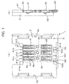
- Fig.1A is a top plan view showing an electrical connector 1 of the invention
- Fig.1B is a sectional view thereof
- Fig.2 is a bottom plan view showing the electrical connector 1 of the invention
- Fig.3A is a top plan view showing a first connecting terminal
- Fig.3B is a sectional view thereof.
- the electrical connector 1 is molded from an insulating plastic material with metal connecting terminals inserted therein. A portion consisting of the plastic material is referred to as a connector housing 2.
- the connector housing 2 is formed in the shape of a flat plate, which is formed with grooves 2a, 2b on opposite sides thereof for guiding the insertion of a card holder 3 (see Fig.4).
- the card holder 3 retains a memory card 6 (see Fig.4) such as a SIM (Subscriber Identity Module) card.
- SIM Subscriber Identity Module
- the connector housing 2 has 6 connecting terminals 4a to 4f mounted to one side thereof. Exposed portions at proximal ends of the connecting portions 4a to 4f (the upper side as seen in Fig.1) are folded to define respective steps for connection with a circuit board in an apparatus body (hereinafter, the folded portions will be referred to as "proximal connecting portions 41a to 41f" or collectively as a “proximal connecting portion 41”).
- the proximal connecting portions 41a to 41f are cream-soldered to metal terminals of a circuit board 5 (see Fig.4). Besides the soldering, any other method such as ultrasonic depositioning may be used to bond the connecting portions to the metal terminals.
- the connecting terminals 4a to 4f are classified into two types including first connecting terminals 4a, 4c, 4e and second connecting terminals 4b, 4d, 4f.
- the first and second connecting terminals are alternately arranged in the connector housing 2.
- the first connecting terminals 4a, 4c, 4e are formed in such a length as to reach a lower side of the connector housing 2 (the lower side as seen in Fig.1), whereas the second connecting terminals 4b, 4d, 4f are formed in about a half the length of the first connecting terminals 4a, 4c, 4e.
- the second connecting terminals 4b, 4d, 4f have their portions close to the proximal connecting portions 41b, 41d, 41f embedded in a resin 2c of the connector housing 2 so as to be retained by the connector housing.
- the second connecting terminals have their distal ends folded in a bellows shape.
- first connecting terminals 4a, 4c, 4e are retained by the connector housing 2 as mostly embedded in the resin 2c of the connector housing except for the proximal connecting portions 41a, 41c, 41e and distal connecting portions thereof (to be described hereinlater), as shown in the top plan view (Fig.1A).
- the first connecting terminals 4a, 4c, 4e each have a portion 43 thereof folded in the bellows shape, the folded portion extending from place about 3/4 of the overall length of the connecting terminal from the proximal end thereof.
- projecting portions defined by distal ends of unfolded base metal portions of the first connecting terminals are so folded as to define respective steps to be soldered to the circuit board, similarly to the aforesaid proximal connecting portion 41.
- the folded projecting portions at the distal ends will hereinafter be referred to as “distal connecting portions 42a, 42c, 42e" or collectively as a “distal connecting portion 42".
- the distal connecting portion 42a and the proximal connecting portion 41a are located in an anteroposterior relation with respect to an insertion direction A (see Fig.1A).
- the distal connecting portion 42c and the proximal connecting portion 41c are also located in the anteroposterior relation with respect to the insertion direction A.
- the distal connecting portion 42e and the proximal connecting portion 41e are also located in the anteroposterior relation with respect to the insertion direction A.
- the bellows-shape portions of the 6 connecting terminals 4a to 4f are all folded in a direction parallel to the insertion direction A of the memory card.
- a fold-back of the bellows shape is located on a side from which the memory card is inserted.
- the distal connectingportions 42a, 42e of the first connecting terminals 4a, 4e on the laterally opposite sides are folded as exposed from respective windows 2d formed in the connector housing 2.
- the first connecting terminal 4c located centrally between the above first connecting terminals, is not provided with a window. This is because if all the connecting terminals 4a, 4c, 4e are to be exposed, the connector housing 2 must be formed with 3 sequential windows for exposing the terminals, which in turn, reduce the strength of the connector housing 2.
- the distal connecting portion 42c of the central first connecting terminal 4c is also folded to be exposed from a bottom surface of the connector housing 2, thus adapted to be connected with the circuit board.
- Fig.4 is a sectional view showing the electrical connector 1 under service condition.
- the insertion direction of a card is represented by an arrow A.
- the electrical connector 1 has the proximal connecting portion 41 and the distal connecting portion 42 thereof connected with the metal terminals of the circuit board 5, thereby being fixed to the circuit board 5 in the apparatus body.
- the metal terminal of the circuit board 5 in connected relation with the proximal connecting portion 41 must be connected with a circuit component of the apparatus body, whereas the metal terminal in connected relation with the distal connecting portion 42 may not necessarily be connected with a circuit component of the apparatus body or may be electrically isolated from the others. This is because an electrical connection established at one place of the connecting terminal fully serves the purpose.
- an arrangement may be made such that the metal terminal of the circuit board 5 in connected relation with the distal connecting portion 42 is connected with the circuit component of the apparatus body while the metal terminal in connected relation with the proximal connecting portion 41 is not connected with the circuit component of the apparatus body.
- the first connecting terminals 4a, 4c, 4e have not only their proximal connecting portions 41a, 41c, 41e but also their distal connecting portions 41a, 42c, 42e connected with the circuit board. Furthermore, the first connecting terminals 4a, 4c, 4e are retained by the connector housing as embedded in the resin thereof. Therefore, the connector housing 2 itself is prevented from encountering lift-off from the circuit board 5.
- the second connecting terminals 4b, 4d, 4f have the conventional cantilevered bellows structure, they are believed to cause no problem because the first connecting terminals 4a, 4c, 4e prevent the connector housing 2 from being lifted off from the circuit board.
Landscapes
- Engineering & Computer Science (AREA)
- Artificial Intelligence (AREA)
- Computer Vision & Pattern Recognition (AREA)
- Physics & Mathematics (AREA)
- General Physics & Mathematics (AREA)
- Theoretical Computer Science (AREA)
- Coupling Device And Connection With Printed Circuit (AREA)
- Multi-Conductor Connections (AREA)
Abstract
Description
Claims (5)
- An electrical connector mounted to a circuit board in an apparatus body and retaining a memory card thereby establishing electrical connection between the memory card and a circuit component in the apparatus body,
the electrical connector comprising a connector housing for receiving and retaining the memory card, and a connecting terminal fixed in the connector housing,
wherein the connecting terminal has a portion capable of electrically contacting the memory card retained by the connector housing, and includes at least 2 portions connected with the circuit board to which the electrical connector is mounted. - An electrical connector according to Claim 1, wherein a plurality of the connecting terminals are fixed in the connector housing and at least one of the connecting terminals includes at least 2 portions connected with the circuit board.
- An electrical connector according to Claim 1 or 2, wherein the connecting terminal includes at least 2 portions connected with the circuit board to which the electrical connector is mounted, the 2 portions located in anteroposterior relation with respect to the portion capable of electrically contacting the memory card.
- An electrical connector according to any one of Claims 1 to 3, wherein at least the 2 portions connected with the circuit board are located in anteroposterior relation with respect to an insertion direction of the memory card.
- An electrical connector according to Claim 4, wherein out of at least the 2 portions connected with the circuit board, a portion located rearwardly with respect to the insertion direction of the memory card is electrically connected with the circuit component, whereas a portion located forwardly with respect to the insertion direction of the memory card is not electrically connected with the circuit component.
Applications Claiming Priority (3)
| Application Number | Priority Date | Filing Date | Title |
|---|---|---|---|
| JP2001278487 | 2001-09-13 | ||
| JP2001278487A JP4806499B2 (en) | 2001-09-13 | 2001-09-13 | Electrical connector |
| PCT/JP2002/009321 WO2003026073A1 (en) | 2001-09-13 | 2002-09-12 | Electric connector |
Publications (3)
| Publication Number | Publication Date |
|---|---|
| EP1427062A1 true EP1427062A1 (en) | 2004-06-09 |
| EP1427062A4 EP1427062A4 (en) | 2006-06-07 |
| EP1427062B1 EP1427062B1 (en) | 2009-12-16 |
Family
ID=19102848
Family Applications (1)
| Application Number | Title | Priority Date | Filing Date |
|---|---|---|---|
| EP02798826A Expired - Lifetime EP1427062B1 (en) | 2001-09-13 | 2002-09-12 | Electric connector |
Country Status (8)
| Country | Link |
|---|---|
| US (1) | US6939176B2 (en) |
| EP (1) | EP1427062B1 (en) |
| JP (1) | JP4806499B2 (en) |
| KR (1) | KR20040028768A (en) |
| CN (1) | CN1264251C (en) |
| DE (1) | DE60234779D1 (en) |
| TW (1) | TW564579B (en) |
| WO (1) | WO2003026073A1 (en) |
Families Citing this family (6)
| Publication number | Priority date | Publication date | Assignee | Title |
|---|---|---|---|---|
| KR100686216B1 (en) | 2004-08-09 | 2007-02-23 | 주식회사 두레디앤이 | Card connection device for mobile phone |
| JP4386811B2 (en) | 2004-08-19 | 2009-12-16 | 日本圧着端子製造株式会社 | Memory card socket |
| JP4403040B2 (en) | 2004-08-19 | 2010-01-20 | 日本圧着端子製造株式会社 | Card holder for SIM socket |
| JP4385047B2 (en) | 2006-12-06 | 2009-12-16 | ホシデン株式会社 | Contact and card adapter and card connector provided therewith |
| CN201285850Y (en) * | 2008-09-09 | 2009-08-05 | 富士康(昆山)电脑接插件有限公司 | Electric connector |
| JP5738689B2 (en) * | 2011-06-21 | 2015-06-24 | モレックス インコーポレイテドMolex Incorporated | Card connector |
Family Cites Families (16)
| Publication number | Priority date | Publication date | Assignee | Title |
|---|---|---|---|---|
| JPS5274459U (en) * | 1975-12-02 | 1977-06-03 | ||
| JPS62101266U (en) * | 1985-12-13 | 1987-06-27 | ||
| JP2891707B2 (en) * | 1988-04-26 | 1999-05-17 | アンプ インコーポレーテッド | Electrical connector |
| JPH06139414A (en) * | 1992-10-28 | 1994-05-20 | Sony Corp | Ic card detecting device |
| DE4243076C2 (en) * | 1992-12-18 | 2000-08-31 | Amphenol Tuchel Elect | Kotaktiereinrichtung for a chip card |
| FR2726694B1 (en) * | 1994-11-07 | 1996-12-06 | Itt Composants Instr | ELECTRICAL CONNECTOR FOR AN ELECTRONIC MEMORY CARD COMPRISING ELECTRICAL CONNECTION MEANS OF THE INSULATOR DISPLACEMENT TYPE |
| US6326568B2 (en) * | 1997-07-02 | 2001-12-04 | Molex Incorporated | Blade switch assembly for a card reader |
| JPH1186978A (en) * | 1997-09-03 | 1999-03-30 | Dai Ichi Denshi Kogyo Kk | Electric connector for ic card |
| FR2773275B1 (en) * | 1997-12-26 | 2000-01-28 | Itt Mfg Enterprises Inc | VERY LOW THICKNESS ELECTRICAL CONNECTOR FOR CONNECTION OF AN ELECTRONIC MEMORY CARD |
| JP3295715B2 (en) * | 1997-12-26 | 2002-06-24 | 日本圧着端子製造株式会社 | Printed wiring board connector and method of manufacturing the same |
| FR2773244B1 (en) * | 1997-12-26 | 2000-01-28 | Itt Mfg Enterprises Inc | SWITCH FOR DETECTING THE PRESENCE OF AN ELECTRONIC MEMORY CARD IN A READ-WRITE DEVICE |
| JPH11297431A (en) * | 1998-04-08 | 1999-10-29 | Amp Japan Ltd | Electrical connector |
| TW429652B (en) * | 1999-12-23 | 2001-04-11 | Hon Hai Prec Ind Co Ltd | Electric connector terminal |
| TW474496U (en) * | 2000-12-20 | 2002-01-21 | Hon Hai Prec Ind Co Ltd | Electronic card connector |
| JP2002280098A (en) * | 2001-03-21 | 2002-09-27 | Hirose Electric Co Ltd | Card connector |
| JP2004103491A (en) * | 2002-09-12 | 2004-04-02 | Honda Tsushin Kogyo Co Ltd | Surface mount type connector |
-
2001
- 2001-09-13 JP JP2001278487A patent/JP4806499B2/en not_active Expired - Fee Related
-
2002
- 2002-09-12 EP EP02798826A patent/EP1427062B1/en not_active Expired - Lifetime
- 2002-09-12 DE DE60234779T patent/DE60234779D1/en not_active Expired - Lifetime
- 2002-09-12 KR KR10-2003-7015713A patent/KR20040028768A/en not_active Ceased
- 2002-09-12 CN CNB028171691A patent/CN1264251C/en not_active Expired - Fee Related
- 2002-09-12 US US10/486,500 patent/US6939176B2/en not_active Expired - Lifetime
- 2002-09-12 WO PCT/JP2002/009321 patent/WO2003026073A1/en not_active Ceased
- 2002-09-13 TW TW091120978A patent/TW564579B/en not_active IP Right Cessation
Also Published As
| Publication number | Publication date |
|---|---|
| CN1550054A (en) | 2004-11-24 |
| US20040209519A1 (en) | 2004-10-21 |
| CN1264251C (en) | 2006-07-12 |
| DE60234779D1 (en) | 2010-01-28 |
| TW564579B (en) | 2003-12-01 |
| US6939176B2 (en) | 2005-09-06 |
| KR20040028768A (en) | 2004-04-03 |
| EP1427062B1 (en) | 2009-12-16 |
| EP1427062A4 (en) | 2006-06-07 |
| WO2003026073A1 (en) | 2003-03-27 |
| JP4806499B2 (en) | 2011-11-02 |
| JP2003086275A (en) | 2003-03-20 |
Similar Documents
| Publication | Publication Date | Title |
|---|---|---|
| US7819703B1 (en) | Electrical connector configured by wafer having coupling lead-frame and method for making the same | |
| DK1289076T3 (en) | Coaxial connector for connecting circuit boards | |
| EP0926780B1 (en) | A connector for a printed circuit board and a production method therefor | |
| EP0746062B1 (en) | Surface engageable electrical connector | |
| US6508661B1 (en) | Flexible printed circuit connector | |
| US20050112947A1 (en) | Connector for memory cards | |
| EP0696086B1 (en) | Sealed receptacle connector for PC card | |
| US6224409B1 (en) | Audio jack | |
| US7413476B2 (en) | Electrical interconnection with mating terminals | |
| US5542853A (en) | Shunted electrical connector | |
| EP1361627B1 (en) | Connector which can be simplified in structure of an end portion in a card inserting/removing direction | |
| US7044798B2 (en) | Card connector | |
| US6652302B1 (en) | Electrical connector with pivotable contact | |
| US6939176B2 (en) | Electrical connector | |
| WO2010039904A2 (en) | Component-to-board electrical connector | |
| US6793533B2 (en) | Electrical connector assembly | |
| JP2007250324A (en) | Card connector | |
| WO2002023235A3 (en) | Optical waveguide socket, optical waveguide plug, and optical waveguide socket assembly | |
| US5997356A (en) | Electronic card connector having card-biasing means | |
| CN221150340U (en) | Coupling arrangement for coupling a terminal connector to a circuit board arrangement | |
| US7402054B2 (en) | Board-to-board connector | |
| JPH0785933A (en) | Movable connector | |
| KR100191746B1 (en) | Classified Electrical Connectors | |
| US7753694B2 (en) | Stacked card connector | |
| KR100852149B1 (en) | Plug connector for mobile communication terminal |
Legal Events
| Date | Code | Title | Description |
|---|---|---|---|
| PUAI | Public reference made under article 153(3) epc to a published international application that has entered the european phase |
Free format text: ORIGINAL CODE: 0009012 |
|
| 17P | Request for examination filed |
Effective date: 20031105 |
|
| AK | Designated contracting states |
Kind code of ref document: A1 Designated state(s): AT BE CH CY DE DK ES FI FR GB GR IE IT LI LU MC NL PT SE TR |
|
| A4 | Supplementary search report drawn up and despatched |
Effective date: 20060425 |
|
| RIC1 | Information provided on ipc code assigned before grant |
Ipc: H01R 13/00 20060101ALI20060420BHEP Ipc: G06K 17/00 20060101ALI20060420BHEP Ipc: H01R 12/32 20060101ALI20060420BHEP Ipc: H01R 12/22 20060101ALI20060420BHEP Ipc: H01R 12/18 20060101AFI20030403BHEP |
|
| 17Q | First examination report despatched |
Effective date: 20060811 |
|
| 17Q | First examination report despatched |
Effective date: 20060811 |
|
| GRAP | Despatch of communication of intention to grant a patent |
Free format text: ORIGINAL CODE: EPIDOSNIGR1 |
|
| RBV | Designated contracting states (corrected) |
Designated state(s): DE FR GB IT |
|
| GRAS | Grant fee paid |
Free format text: ORIGINAL CODE: EPIDOSNIGR3 |
|
| GRAA | (expected) grant |
Free format text: ORIGINAL CODE: 0009210 |
|
| RIN1 | Information on inventor provided before grant (corrected) |
Inventor name: YOKOYAMA, HIROMASAC/O TOKYO ENGINEERING CENTER |
|
| AK | Designated contracting states |
Kind code of ref document: B1 Designated state(s): DE FR GB IT |
|
| REG | Reference to a national code |
Ref country code: GB Ref legal event code: FG4D |
|
| REF | Corresponds to: |
Ref document number: 60234779 Country of ref document: DE Date of ref document: 20100128 Kind code of ref document: P |
|
| PLBE | No opposition filed within time limit |
Free format text: ORIGINAL CODE: 0009261 |
|
| STAA | Information on the status of an ep patent application or granted ep patent |
Free format text: STATUS: NO OPPOSITION FILED WITHIN TIME LIMIT |
|
| 26N | No opposition filed |
Effective date: 20100917 |
|
| PGFP | Annual fee paid to national office [announced via postgrant information from national office to epo] |
Ref country code: FR Payment date: 20100921 Year of fee payment: 9 |
|
| PGFP | Annual fee paid to national office [announced via postgrant information from national office to epo] |
Ref country code: GB Payment date: 20100908 Year of fee payment: 9 |
|
| PG25 | Lapsed in a contracting state [announced via postgrant information from national office to epo] |
Ref country code: IT Free format text: LAPSE BECAUSE OF NON-PAYMENT OF DUE FEES Effective date: 20100912 |
|
| REG | Reference to a national code |
Ref country code: DE Ref legal event code: R119 Ref document number: 60234779 Country of ref document: DE Effective date: 20110401 |
|
| PG25 | Lapsed in a contracting state [announced via postgrant information from national office to epo] |
Ref country code: DE Free format text: LAPSE BECAUSE OF NON-PAYMENT OF DUE FEES Effective date: 20110401 |
|
| GBPC | Gb: european patent ceased through non-payment of renewal fee |
Effective date: 20110912 |
|
| REG | Reference to a national code |
Ref country code: FR Ref legal event code: ST Effective date: 20120531 |
|
| PG25 | Lapsed in a contracting state [announced via postgrant information from national office to epo] |
Ref country code: GB Free format text: LAPSE BECAUSE OF NON-PAYMENT OF DUE FEES Effective date: 20110912 Ref country code: FR Free format text: LAPSE BECAUSE OF NON-PAYMENT OF DUE FEES Effective date: 20110930 |