EP1427019A1 - Image detection device - Google Patents
Image detection device Download PDFInfo
- Publication number
- EP1427019A1 EP1427019A1 EP02762838A EP02762838A EP1427019A1 EP 1427019 A1 EP1427019 A1 EP 1427019A1 EP 02762838 A EP02762838 A EP 02762838A EP 02762838 A EP02762838 A EP 02762838A EP 1427019 A1 EP1427019 A1 EP 1427019A1
- Authority
- EP
- European Patent Office
- Prior art keywords
- light
- face
- outer peripheral
- fiber optical
- optical block
- Prior art date
- Legal status (The legal status is an assumption and is not a legal conclusion. Google has not performed a legal analysis and makes no representation as to the accuracy of the status listed.)
- Granted
Links
Images

Classifications
-
- G—PHYSICS
- G02—OPTICS
- G02B—OPTICAL ELEMENTS, SYSTEMS OR APPARATUS
- G02B6/00—Light guides; Structural details of arrangements comprising light guides and other optical elements, e.g. couplings
- G02B6/04—Light guides; Structural details of arrangements comprising light guides and other optical elements, e.g. couplings formed by bundles of fibres
- G02B6/06—Light guides; Structural details of arrangements comprising light guides and other optical elements, e.g. couplings formed by bundles of fibres the relative position of the fibres being the same at both ends, e.g. for transporting images
- G02B6/08—Light guides; Structural details of arrangements comprising light guides and other optical elements, e.g. couplings formed by bundles of fibres the relative position of the fibres being the same at both ends, e.g. for transporting images with fibre bundle in form of plate
-
- G—PHYSICS
- G02—OPTICS
- G02B—OPTICAL ELEMENTS, SYSTEMS OR APPARATUS
- G02B6/00—Light guides; Structural details of arrangements comprising light guides and other optical elements, e.g. couplings
- G02B6/24—Coupling light guides
- G02B6/42—Coupling light guides with opto-electronic elements
- G02B6/4201—Packages, e.g. shape, construction, internal or external details
- G02B6/4202—Packages, e.g. shape, construction, internal or external details for coupling an active element with fibres without intermediate optical elements, e.g. fibres with plane ends, fibres with shaped ends, bundles
- G02B6/4203—Optical features
-
- H—ELECTRICITY
- H10—SEMICONDUCTOR DEVICES; ELECTRIC SOLID-STATE DEVICES NOT OTHERWISE PROVIDED FOR
- H10F—INORGANIC SEMICONDUCTOR DEVICES SENSITIVE TO INFRARED RADIATION, LIGHT, ELECTROMAGNETIC RADIATION OF SHORTER WAVELENGTH OR CORPUSCULAR RADIATION
- H10F39/00—Integrated devices, or assemblies of multiple devices, comprising at least one element covered by group H10F30/00, e.g. radiation detectors comprising photodiode arrays
- H10F39/011—Manufacture or treatment of image sensors covered by group H10F39/12
-
- G—PHYSICS
- G02—OPTICS
- G02B—OPTICAL ELEMENTS, SYSTEMS OR APPARATUS
- G02B6/00—Light guides; Structural details of arrangements comprising light guides and other optical elements, e.g. couplings
- G02B6/04—Light guides; Structural details of arrangements comprising light guides and other optical elements, e.g. couplings formed by bundles of fibres
- G02B6/06—Light guides; Structural details of arrangements comprising light guides and other optical elements, e.g. couplings formed by bundles of fibres the relative position of the fibres being the same at both ends, e.g. for transporting images
Definitions
- This invention relates to an image sensing device provided with a fiber optical block.
- an image sensing device capable of detecting a two-dimensional image (optical image)
- an image sensing device which directly, optically connects a fiber optical block having a light outputting end face tilted with respect to the optical axes of optical fibers to a light-receiving surface of a solid-state image pickup device.
- Such an image sensing device has been employed in, for example, a fingerprint detector capable of obtaining a high-quality fingerprint image.
- a solid-state image pickup device As image sensing devices which detect a two-dimensional image by an output light from a fiber optical block by use of a solid-state image pickup device, provided are devices as disclosed in, for example, Japanese Patent Application Laid-Open No. H-7-211877, Japanese Patent Application Laid-Open No. H-7-174947, and Japanese Patent Application Laid-Open No. H-10-12851.
- a device generally, in a solid-state image pickup device with a fiber optical block connected, a plurality of electrode pads are provided on the outer periphery of a light-receiving surface thereof. And, to each of the plurality of electrode pads, a connection wire (bonding wire) is electrically connected.
- a sectional shape of the fiber optical block is a parallelogram
- electrode pads arranged on an outer peripheral portion positioned in a tilting direction of the optical axes of the optical fibers with respect to the light-receiving surface are considered, there is a possibility that contact between a slope part of the fiber optical block protruding from the light-receiving surface to the outer peripheral portion and connection wires connected to the electrode pads may result in breaking of the connection wires.
- a construction can be considered wherein, by shortening the length of the fiber optical block in the direction to protrude to the outer peripheral portion, the distance between the slope part of the fiber optical block and the electrode pads and connection wires of the solid-state image pickup device is provided with an allowance.
- the area of the light outputting end face of the fiber optical block narrows for the light-receiving surface of the solid-state image pickup device. Accordingly, an effective area of the light-receiving surface, which is a region where a light outputted from the fiber optical block is inputted in the light-receiving surface, becomes narrow.
- the present invention has been made to solve the above problems and an object thereof is to provide an image sensing device which can favorably combine both the electrode pads and connection wires of the solid-state image pickup device and the fiber optical block tilted with respect to the light-receiving surface.
- an image sensing device comprises: (1) a fiber optical block in which a plurality of optical fibers are arrayed so that their optical axes become substantially parallel to each other, which is formed so that a two-dimensional image inputted from a light inputting end face is transmitted to a light outputting end face, and in which the light outputting end face is tilted at a predetermined angle ⁇ of an acute angle with respect to the optical axes; and (2) a solid-state image pickup device having a light-receiving portion with two-dimensional pixel array to whose light-receiving surface the light outputting end face of the fiber optical block is optically connected, and a plurality of electrode pads arranged on a surface identical to the light-receiving surface and on outer peripheral portions thereof, wherein (3) the fiber optical block is arranged so that, when viewed from the light-receiving surface, the optical axes are tilted at the predetermined angle ⁇ toward a first side out of four sides
- the light-receiving surface of the solid-state image pickup device and the light outputting end face of the fiber optical block tilted with respect to the optical axes are optically connected.
- This fiber optical block is arranged so that, when viewed from the light-receiving surface, the optical axes are tilted at a predetermined angle ⁇ toward the first side of the light-receiving surface. Morever, no electrode pads are provided on a first outer peripheral portion facing the first side. Accordingly, it is possible to favorably combine both the electrode pads and connection wires of the solid-state image pickup device and the fiber optical block tilted with respect to the light-receiving surface.
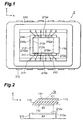
- Fig. 1 is a plan view showing an image sensing device according to a first embodiment.
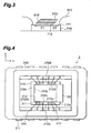
- Fig. 2 shows a part of a side sectional view of the image sensing device 1 shown in Fig. 1.
- two mutually perpendicular directions along a pixel array on a light-receiving surface of a solid-state image pickup device are provided as an x-direction and a y-direction, and a vertical direction perpendicular to the x-axis and y-axis is provided as a z-axis direction.
- the side sectional view of Fig. 2 is a sectional view at an xz-plane viewed from the y-axis direction.
- the fiber optical block 110 and solid-state image pickup device 210 to be mutually connected are shown in a manner exploded in the z-axis direction.
- the image sensing device 1 comprises a fiber optical block 110 and a solid-state image pickup device 210 and is constructed so that a two-dimensional image (two-dimensional optical image) can be detected.
- the fiber optical block 110 is formed by integrating a plurality of optical fibers 113 arrayed so that the optical axes become substantially parallel to each other. Thereby, the fiber optical block 110 can transmit a two-dimensional image inputted from one end face to the other end face along the optical axes.
- an end face located upward in terms of the z-axis direction is provided as a light inputting end face 111
- an end face located downward and opposed to the light inputting end face 111 is provided as a light outputting end face 112.
- the light inputting end face 111 and light outputting end face 112 both have substantially identically formed rectangular shapes.
- the oblique lines illustrated in a section of the fiber optical block 110 show tilting directions of the optical axes of the optical fibers 113.
- the light outputting end face 112 is tilted at a predetermined angle ⁇ of an acute angle with respect to the optical axes of the optical fibers 113.
- This tilting angle ⁇ is set to 36°, for example.
- the light inputting end face 111 is also tilted at an angle ⁇ with respect to the optical axes of the optical fibers 113, and the light outputting end face 112 and light inputting end face 111 are substantially parallel.
- a sectional shape of the fiber optical block 110 viewed from the y-axis direction is, as shown in Fig. 2, a substantially parallelogram shape whose two sides extending from the light outputting end face 112 to the light inputting end face 111 are substantially parallel to the optical axes of the optical fibers 113.
- a region where a light inputted from a light inputting end face is outputted is provided as an output region and a region excluding the same where a light inputted from a light inputting end face is not outputted is provided as a non-output region.
- the fiber optical block 110 of the present embodiment because of the above-described sectional shape, in contrast to the whole of the light inputting end face 111 as an input region C1, the whole of the light outputting end face 112 becomes an output region B1.
- the solid-state image pickup device 210 has a light-receiving portion 212 with a light-receiving surface 212e of a rectangular shape, and with pixels two-dimensionally arrayed along the x-axis direction and y-axis direction.
- the part shown at an upper-surface side of the solid-state image pickup device 210 by alternative long and short dash lines is the light-receiving surface 212e.
- a plurality of electrode pads 211 for inputting and outputting signals with respect to respective portions of the solid-state image pickup device 210 such as a light-receiving portion 212 are provided.
- the respective portions of the solid-state image pickup device 210 are electrically connected to their respectively corresponding electrode pads 211 by signal lines (unillustrated).
- the above-described light outputting end face 112 of the fiber optical block 110 is optically connected.
- the solid-state image pickup device 210 to which the fiber optical block 110 is connected, is placed on a substrate 310.
- a substrate 310 On the substrate 310, at predetermined positions on an outer peripheral side of a surface where the solid-state image pickup device 210 is to be placed, a plurality of internal electrode terminals 311 respectively corresponding to the electrode pads 211 of the solid-state image pickup device 210 are arranged. These internal electrode terminals 311 are electrically connected to external electrode terminals 312 for external connection, which are arranged on side surfaces of the substrate 310, by internal wirings (unillustrated) through the substrate 310. Then, the solid-state image pickup device 210 is placed on the substrate 310 so that the respectively corresponding electrode pads 211 and internal electrode terminals 311 are close together. In addition, each of the mutually corresponding electrode pads 211 and internal electrode terminals 311 is electrically connected by a connection wire 410.
- the light-receiving surface 212e of the solid-state image pickup device 210 is surrounded by four sides of two sides 212a and 212c which are parallel to the y-axis and opposed in the x-axis direction and two sides 212b and 212d which are parallel to the x-axis and opposed in the y-axis direction.
- the fiber optical block 110 is arranged so that, when viewed from the light-receiving surface 212e, the optical axes of the optical fibers 113 are tilted at the aforementioned angle ⁇ toward the side 212a (first side) out of the four sides 212a-212d. Thereby, a tilting direction of the optical axes of the fiber optical block 110 is in a positive direction of the x-axis.
- each of the plurality of electrode pads 211 is arranged on two outer peripheral portions 210b and 210d adjacent to a first outer peripheral portion 210a facing the side 212a.
- the light outputting end face 112 of the fiber optical block 110 and the light-receiving surface 212e of the solid-state image pickup device 210 have in either case a rectangular shape as mentioned above, and these are substantially identically formed to each other.
- the light outputting end face 112 and light-receiving surface 212e are connected so that their surfaces substantially coincide with each other.
- a region to which an output region in a light outputting end face of a fiber optical block is connected is provided as an effective region, and a region excluding the same is provided as an insensitive region.
- a whole region A1 of the light-receiving surface 212e becomes an effective region.
- a two-dimensional image inputted from the light inputting end face 111 is transmitted to the light outputting end face 112 along the optical axes of the optical fibers 113. Then, the two-dimensional image outputted from the whole of the light outputting end face 112 as an output region is inputted from the light-receiving surface 212e of the solid-state image pickup device 210 into the light-receiving portion 212 and is detected at the respective pixels of the light-receiving portion 212. Obtained detection signals are outputted, through the outputting electrode pads 211, connection wires 410, and internal electrode terminals 311, from the external electrode terminals 312.
- each of the plurality of electrode pads 211 arranged on the outer periphery of the light-receiving portion 212 is provided not on the first outer peripheral portion 210a positioned in the tilting direction of the optical axes of the optical fibers 113, but on the mutually opposed two outer peripheral portions 210b and 210d adjacent to the outer peripheral portion 210a.
- the tilting direction of the optical axes of the optical fibers 113 and the direction in which the electrode pads 211 are arrayed result in an identical direction.
- the fiber optical block 110 whose sectional shape is a parallelogram, contact of the slope part of the fiber optical block 110 protruding from the light-receiving surface 212e to the outer peripheral portion 210a with the connection wires 410 can be avoided. In addition, it is possible to enlarge the effective region A1 of the light-receiving surface 212e.
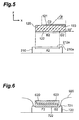
- Fig. 3 is a side sectional view of a conventional image sensing device.
- electrode pads 711 are arrayed, in a solid-state image pickup device 710, on an outer peripheral portion positioned in a direction in which the optical axes of the optical fibers 613 of a fiber optical block 610 are tilted.
- connection wires 910 may result in breaking of the connection wires 910.
- contact with the connection wire 910 is avoided by shortening the length of the fiber optical block 610 in the direction to protrude to the outer peripheral portion, an insensitive region G1 of the light-receiving surface 712 enlarges, therefore, an effective area F1 of the light-receiving surface narrows.
- the image sensing device 1 since the image sensing device 1 according to the present embodiment employs a construction wherein no electrode pads 211 are provided on the outer peripheral portion 210a positioned in the tilting direction of the optical axes of the optical fibers 113, contact between the fiber optical block 110 and connection wires 410 can be avoided. Moreover, since there is no necessity for shortening the length of the fiber optical block 110 in the direction to protrude to the outer peripheral portion 210a so as to avoid contact with the connection wires 410, the effective region A1 of the light-receiving surface 212e of the light-receiving portion 212 can be enlarged.
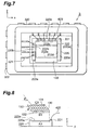
- Fig. 4 is a plan view showing an image sensing device according to a second embodiment.
- Fig. 5 shows a part of a side sectional view of the image sensing device 2 shown in Fig. 4.
- the side sectional view of Fig. 5 is a sectional view at an xz-plane viewed from the y-axis direction.
- a fiber optical block 120 and a solid-state image pickup device 210 to be mutually connected are shown in a manner exploded in the z-axis direction.
- the image sensing device 2 shown in Fig. 4 comprises the fiber optical block 120, the solid-state image pickup device 210, a substrate 310, and connection wires 410. Among these, constructions of the solid-state image pickup device 210, substrate 310, and connection wires 410 are similar to those of the first embodiment.
- the fiber optical block 120 is formed by integrating a plurality of optical fibers 123 arrayed so that the optical axes become substantially parallel to each other. Thereby, the fiber optical block 120 can transmit a two-dimensional image inputted from one end face to the other end face along the optical axes.
- an end face located upward in terms of the z-axis direction is provided as a light inputting end face 121
- an end face located downward and opposed to the light inputting end face 121 is provided as a light outputting end face 122.
- the light inputting end face 121 and light outputting end face 122 both have substantially identically formed rectangular shapes.
- the oblique lines illustrated in a section of the fiber optical block 120 show tilting directions of the optical axes of the optical fibers 123.
- the light outputting end face 122 is tilted at a predetermined angle ⁇ of an acute angle with respect to the optical axes of the optical fibers 123.
- the light inputting end face 121 is also tilted at an angle ⁇ with respect to the optical axes of the optical fibers 123, and the light outputting end face 122 and light inputting end face 121 are substantially parallel.
- a sectional shape of the fiber optical block 120 viewed from the y-axis direction is, as shown in Fig. 5, a substantially rectangular shape whose two sides extending from the light outputting end face 122 to the light inputting end face 121 are substantially vertical to the light outputting end face 122.
- a partial region where a light to be transmitted to the light outputting end face 122 is inputted is an input region C2.
- a partial region where a light inputted from the input region C2 is outputted is an output region B2, and a region excepting the same is a non-output region D2.
- the input region C2 and output region B2 have rectangular shapes substantially identically formed to each other.
- a connecting relationship between the fiber optical block 120 and solid-state image pickup device 210 in the image sensing device 2 shown in Fig. 4 will be described.
- a light-receiving surface 212e of the solid-state image pickup device 210 is surrounded by four sides of two sides 212a and 212c which are parallel to the y-axis and opposed in the x-axis direction and two sides 212b and 212d which are parallel to the x-axis and opposed in the y-axis direction.
- the fiber optical block 120 is arranged so that, when viewed from the light-receiving surface 212e, the optical axes of the optical fibers 123 are tilted at the aforementioned angle ⁇ toward the side 212a out of the four sides 212a-212d. Thereby, a tilting direction of the optical axes of the fiber optical block 120 is in a positive direction of the x-axis.
- each of a plurality of electrode pads 211 is arranged on two outer peripheral portions 210b and 210d adjacent to a first outer peripheral portion 210a facing the side 212a.
- the output region B2 in the light outputting end face 122 of the fiber optical block 120 and the light-receiving surface 212e of the solid-state image pickup device 210 have in either case a rectangular shape as mentioned above, and these are substantially identically formed to each other.
- the output region B2 of the light outputting end face 122 and light-receiving surface 212e are connected so that their surfaces substantially coincide with each other. Thereby, a part on the side of the side 212a of the fiber optical block 120 including the non-output region D2 of the light outputting end face 122 is protruded from above the light-receiving portion 212 toward the outer peripheral portion 210a side.
- a whole region A2 of the light-receiving surface 212e becomes an effective region.
- a two-dimensional image inputted from the input region C2 of the light inputting end face 121 is transmitted to the output region B2 of the light outputting end face 122 along the optical axes of the optical fibers 123.
- the two-dimensional image outputted from the output region B2 of a part of the light outputting end face 122 is inputted from the light-receiving surface 212e of the solid-state image pickup device 210 into the light-receiving portion 212 and is detected at the respective pixels of the light-receiving portion 212.
- Obtained detection signals are outputted, through the outputting electrode pads 211, connection wires 410, and internal electrode terminals 311, from the external electrode terminals 312.
- each of the plurality of electrode pads 211 arranged on the outer periphery of the light-receiving portion 212 is provided not on the first outer peripheral portion 210a positioned in the tilting direction of the optical axes of the optical fibers 123, but on the mutually opposed two outer peripheral portions 210b and 210d adjacent to the outer peripheral portion 210a. Then, the surfaces of the output region B2 and light-receiving surface 212e are connected so as to substantially coincide with each other, thus resulting in a construction wherein the non-output region D2 is protruded to the outer peripheral portion 210a of the light-receiving portion 212. Thereby, it becomes possible to favorably combine both the electrode pads 211 and connection wires 410 of the solid-state image pickup device 210 and the fiber optical block 120 tilted with respect to the light-receiving surface 212e.
- Fig. 6 is a side sectional view of a conventional image sensing device.
- electrode pads 721 are arrayed, in a solid-state image pickup device 720, on an outer peripheral portion positioned in a direction in which the optical axes of the optical fibers 623 of a fiber optical block 620 are tilted.
- a region to which an output region in a light outputting end face of the fiber optical block 620 is connected is provided as an effective region F2
- a region to which a non-output region is connected is provided as an insensitive region G2. Accordingly, a light outputted from the fiber optical block 620 is not inputted into the whole light-receiving surface 722, therefore, an effective region F2 of the light-receiving surface 722 becomes narrow.
- the image sensing device 2 since the image sensing device 2 according to the present embodiment employs a construction wherein no electrode pads 211 are provided on the outer peripheral portion 210a positioned in the tilting direction of the optical axes of the optical fibers 123, it becomes possible to employ a construction wherein the fiber optical block 120 is protruded toward the outer peripheral portion 210a side, therefore, the effective region A2 of the light-receiving surface 212e of the light-receiving portion 212 can be enlarged.
- Fig. 7 is a plan view showing an image sensing device according to a third embodiment.
- Fig. 8 shows a part of a side sectional view of the image sensing device 3 shown in Fig. 7.
- the side sectional view of Fig. 8 is a sectional view at a yz-plane viewed from the x-axis direction.
- the fiber optical block 130 and solid-state image pickup device 220 to be mutually connected are shown in a manner exploded in the z-axis direction.
- the image sensing device 3 comprises a fiber optical block 130 and a solid-state image pickup device 220 and is constructed so that a two-dimensional image can be detected.
- the fiber optical block 130 is formed by integrating a plurality of optical fibers 133 arrayed so that the optical axes become substantially parallel to each other. Thereby, the fiber optical block 130 can transmit a two-dimensional image inputted from one end face to the other end face along the optical axes.
- an end face located upward in terms of the z-axis direction is provided as a light inputting end face 131
- an end face located downward and opposed to the light inputting end face 131 is provided as a light outputting end face 132.
- the light inputting end face 131 and light outputting end face 132 both have substantially identically formed rectangular shapes.
- the oblique lines illustrated in a section of the fiber optical block 130 show tilting directions of the optical axes of the optical fibers 133.
- the light outputting end face 132 is tilted at a predetermined angle ⁇ of an acute angle with respect to the optical axes of the optical fibers 133.
- the light inputting end face 131 is also tilted at an angle ⁇ with respect to the optical axes of the optical fibers 133, and the light outputting end face 132 and light inputting end face 131 are substantially parallel.
- a sectional shape of the fiber optical block 130 viewed from the x-axis direction is, as shown in Fig. 8, a substantially parallelogram shape whose two sides extending from the light outputting end face 132 to the light inputting end face 131 are substantially parallel to the optical axes of the optical fibers 133.
- the whole of the light outputting end face 132 becomes an output region B3.
- the solid-state image pickup device 220 has a light-receiving portion 222 with a light-receiving surface 222e of a rectangular shape, and with pixels two-dimensionally arrayed along the x-axis direction and y-axis direction. At parts in a surface identical to the light-receiving surface 222e and on its outer periphery, a plurality of electrode pads 221 are provided. Then, the respective portions of the solid-state image pickup device 220 are electrically connected to their respectively corresponding electrode pads 221 by signal lines (unillustrated). In addition, to the light-receiving surface 222e, the above-described light outputting end face 132 of the fiber optical block 130 is optically connected.
- the solid-state image pickup device 220 to which the fiber optical block 130 is connected, is placed on a substrate 320.
- a plurality of internal electrode terminals 321 respectively corresponding to the electrode pads 221 of the solid-state image pickup device 220 are arranged.
- These internal electrode terminals 321 are electrically connected to external electrode terminals 322 for external connection, which are arranged on side surfaces of the substrate 320, by internal wirings (unillustrated) through the substrate 320.
- the solid-state image pickup device 220 is placed on the substrate 320 so that the respectively corresponding electrode pads 221 and internal electrode terminals 321 are close together.
- each of the mutually corresponding electrode pads 221 and internal electrode terminals 321 is electrically connected by a connection wire 420.
- the light-receiving surface 222e of the solid-state image pickup device 220 is surrounded by four sides of two sides 222a and 222c which are parallel to the x-axis and opposed in the y-axis direction and two sides 222b and 222d which are parallel to the y-axis and opposed in the x-axis direction.
- the fiber optical block 130 is arranged so that, when viewed from the light-receiving surface 222e, the optical axes of the optical fibers 133 are tilted at the aforementioned angle ⁇ toward the side 222a out of the four sides 222a-222d. Thereby, a tilting direction of the optical axes of the fiber optical block 130 is in a negative direction of the y-axis.
- each of the plurality of electrode pads 221 is arranged on an outer peripheral portion 220b adjacent to a first outer peripheral portion 220a facing the side 222a, and on an outer peripheral portion 220c opposed to the first outer peripheral portion 220a.
- the light outputting end face 132 of the fiber optical block 130 and the light-receiving surface 222e of the solid-state image pickup device 220 have in either case a rectangular shape as mentioned above, and these are substantially identically formed to each other.
- the light outputting end face 132 and light-receiving surface 222e are connected so that their surfaces substantially coincide with each other.
- a whole region A3 of the light-receiving surface 222e becomes an effective region.
- each of the plurality of electrode pads 221 arranged on the outer periphery of the light-receiving portion 222 is provided not on the first outer peripheral portion 220a positioned in the tilting direction of the optical axes of the optical fibers 133, but on an outer peripheral portion 220b adjacent to the outer peripheral portion 220a and an outer peripheral portion 220c opposed to the outer peripheral portion 220a.
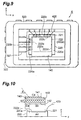
- Fig. 9 is a plan view showing an image sensing device according to a fourth embodiment.
- Fig. 10 shows a part of a side sectional view of the image sensing device 4 shown in Fig. 9.
- the side sectional view of Fig. 10 is a sectional view at a yz-plane viewed from the x-axis direction.
- a fiber optical block 140 and a solid-state image pickup device 220 to be mutually connected are shown in a manner exploded in the z-axis direction.
- the image sensing device 4 shown in Fig. 9 comprises the fiber optical block 140, the solid-state image pickup device 220, a substrate 320, and connection wires 420. Among these, constructions of the solid-state image pickup device 220, substrate 320, and connection wires 420 are similar to those of the third embodiment.
- the fiber optical block 140 is formed by integrating a plurality of optical fibers 143 arrayed so that the optical axes become substantially parallel to each other. Thereby, the fiber optical block 140 can transmit a two-dimensional image inputted from one end face to the other end face along the optical axes.
- an end face located upward in terms of the z-axis direction is provided as a light inputting end face 141
- an end face located downward and opposed to the light inputting end face 141 is provided as a light outputting end face 142.
- the light inputting end face 141 and light outputting end face 142 both have substantially identically formed rectangular shapes.
- the oblique lines illustrated in a section of the fiber optical block 140 show tilting directions of the optical axes of the optical fibers 143.
- the light outputting end face 142 is tilted at a predetermined angle ⁇ of an acute angle with respect to the optical axes of the optical fibers 143.
- the light inputting end face 141 is also tilted at an angle ⁇ with respect to the optical axes of the optical fibers 143, and the light outputting end face 142 and light inputting end face 141 are substantially parallel.
- a sectional shape of the fiber optical block 140 viewed from the x-axis direction is, as shown in Fig. 10, a substantially rectangular shape whose two sides extending from the light outputting end face 142 to the light inputting end face 141 are substantially vertical to the light outputting end face 142.
- a partial region where a light to be transmitted to the light outputting end face 142 is inputted is an input region C4.
- a partial region where a light inputted from the input region C4 is outputted is an output region B4, and a region excepting the same is a non-output region D4.
- the input region C4 and output region B4 have rectangular shapes substantially identically formed to each other.
- a connecting relationship between the fiber optical block 140 and solid-state image pickup device 220 in the image sensing device 4 shown in Fig. 9 will be described.
- a light-receiving surface 222e of the solid-state image pickup device 220 is surrounded by four sides of two sides 222a and 222c which are parallel to the x-axis and opposed in the y-axis direction and two sides 222b and 222d which are parallel to the y-axis and opposed in the x-axis direction.
- the fiber optical block 140 is arranged so that, when viewed from the light-receiving surface 222e, the optical axes of the optical fibers 143 are tilted at the aforementioned angle ⁇ toward the side 222a out of the four sides 222a-222d. Thereby, a tilting direction of the optical axes of the fiber optical block 140 is in a negative direction of the y-axis.
- each of a plurality of electrode pads 221 is arranged on an outer peripheral portion 220b adjacent to a first outer peripheral portion 220a facing the side 222a and an outer peripheral portion 220c opposed to the outer peripheral portion 220a.
- the output region B4 in the light outputting end face 142 of the fiber optical block 140 and the light-receiving surface 222e of the solid-state image pickup device 220 have in either case a rectangular shape as mentioned above, and these are substantially identically formed to each other.
- the output region B4 of the light outputting end face 142 and light-receiving surface 222e are connected so that their surfaces substantially coincide with each other. Thereby, a part on the side of the side 222a of the fiber optical block 140 including the non-output region D4 of the light outputting end face 142 is protruded from above the light-receiving portion 222 toward the outer peripheral portion 220a side.
- a whole region A4 of the light-receiving surface 222e becomes an effective region.
- each of the plurality of electrode pads 221 arranged on the outer periphery of the light-receiving portion 222 is provided not on the first outer peripheral portion 220a positioned in the tilting direction of the optical axes of the optical fibers 143, but on the outer peripheral portion 220b adjacent to the outer peripheral portion 220a and on the outer peripheral portion 220c opposed to the outer peripheral portion 220a. Then, the surfaces of the output region B4 and light-receiving surface 222e are connected so as to substantially coincide with each other, thus resulting in a construction wherein the non-output region D4 is protruded to the outer peripheral portion 220a of the light-receiving portion 222. Thereby, it becomes possible to favorably combine both the electrode pads 221 and connection wires 420 of the solid-state image pickup device 220 and the fiber optical block 140 tilted with respect to the light-receiving surface 222e.
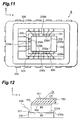
- Fig. 11 is a plan view showing an image sensing device according to a fifth embodiment.
- Fig. 12 shows a part of a side sectional view of the image sensing device 5 shown in Fig. 11.
- the side sectional view of Fig. 12 is a sectional view at an xz-plane viewed from the y-axis direction.
- a fiber optical block 150 and solid-state image pickup device 230 to be mutually connected are shown in a manner exploded in the z-axis direction.
- the image sensing device 5 comprises a fiber optical block 150 and a solid-state image pickup device 230 and is constructed so that a two-dimensional image can be detected.
- the fiber optical block 150 is formed by integrating a plurality of optical fibers 153 arrayed so that the optical axes become substantially parallel to each other. Thereby, the fiber optical block 150 can transmit a two-dimensional image inputted from one end face to the other end face along the optical axes.
- an end face located upward in terms of the z-axis direction is provided as a light inputting end face 151
- an end face located downward and opposed to the light inputting end face 151 is provided as a light outputting end face 152.
- the light inputting end face 151 and light outputting end face 152 both have substantially identically formed rectangular shapes.
- the oblique lines illustrated in a section of the fiber optical block 150 show tilting directions of the optical axes of the optical fibers 153.
- the light outputting end face 152 is tilted at a predetermined angle ⁇ of an acute angle with respect to the optical axes of the optical fibers 153.
- the light inputting end face 151 is also tilted at an angle ⁇ with respect to the optical axes of the optical fibers 153, and the light outputting end face 152 and light inputting end face 151 are substantially parallel.
- a sectional shape of the fiber optical block 150 viewed from the y-axis direction is, as shown in Fig. 12, a substantially parallelogram shape whose two sides extending from the light outputting end face 152 to the light inputting end face 151 are substantially parallel to the optical axes of the optical fibers 153.
- the whole of the light outputting end face 152 becomes an output region B5.
- the solid-state image pickup device 230 has a light-receiving portion 232 with a light-receiving surface 232e of a rectangular shape, and with pixels two-dimensionally arrayed along the x-axis direction and y-axis direction. At parts in a surface identical to the light-receiving surface 232e and on its outer periphery, a plurality of electrode pads 231 are provided. Then, the respective portions of the solid-state image pickup device 230 are electrically connected to their respectively corresponding electrode pads 231 by signal lines (unillustrated). In addition, to the light-receiving surface 232e, the above-described light outputting end face 152 of the fiber optical block 150 is optically connected.
- the solid-state image pickup element 230 to which the fiber optical block 150 is connected, is placed on a substrate 330.
- a plurality of internal electrode terminals 331 respectively corresponding to the electrode pads 231 of the solid-state image pickup device 230 are arranged.
- These internal electrode terminals 331 are electrically connected to external electrode terminals 332 for external connection, which are arranged on side surfaces of the substrate 330, by internal wirings (unillustrated) through the substrate 330.
- the solid-state image pickup device 230 is placed on the substrate 330 so that the respectively corresponding electrode pads 231 and internal electrode terminals 331 are close together.
- each of the mutually corresponding electrode pads 231 and internal electrode terminals 331 is electrically connected by a connection wire 430.
- the light-receiving surface 232e of the solid-state image pickup device 230 is surrounded by four sides of two sides 232a and 232c which are parallel to the y-axis and opposed in the x-axis direction and two sides 232b and 232d which are parallel to the x-axis and opposed in the y-axis direction.
- the fiber optical block 150 is arranged so that, when viewed from said light-receiving surface 232e, the optical axes of the optical fibers 153 are tilted at the aforementioned angle ⁇ toward the side 232a out of the four sides 232a-232d. Thereby, a tilting direction of the optical axes of the fiber optical block 150 is in a positive direction of the x-axis.
- each of the plurality of electrode pads 231 is arranged on two outer peripheral portions 230b and 230d adjacent to a first outer peripheral portion 230a facing the side 232a and on the outer peripheral portion 230c opposed to the first peripheral portion 230a.
- the light outputting end face 152 of the fiber optical block 150 and the light-receiving surface 232e of the solid-state image pickup device 230 have in either case a rectangular shape as mentioned above, and these are substantially identically formed to each other.
- the light outputting end face 152 and light-receiving surface 232e are connected so that their surfaces substantially coincide with each other.
- a whole region A5 of the light-receiving surface 232e becomes an effective region.
- each of the plurality of electrode pads 231 arranged on the outer periphery of the light-receiving portion 232 is provided not on the first outer peripheral portion 230a positioned in the tilting direction of the optical axes of the optical fibers 153, but on the mutually opposed two outer peripheral portion 230b and 230d adjacent to the outer peripheral portion 230a and on the outer peripheral portion 230c opposed to the first outer peripheral portion 230a.
- Fig. 13 is a plan view showing an image sensing device according to a sixth embodiment.
- Fig. 14 shows a part of a side sectional view of the image sensing device 6 shown in Fig. 13.
- the side sectional view of Fig. 14 is a sectional view at an xz-plane viewed from the y-axis direction.
- a fiber optical block 160 and a solid-state image pickup device 230 to be mutually connected are shown in a manner exploded in the z-axis direction.
- the image sensing device 6 shown in Fig. 13 comprises the fiber optical block 160, the solid-state image pickup device 230, a substrate 330, and connection wires 430. Among these, constructions of the solid-state image pickup device 230, substrate 330, and connection wires 430 are similar to those of the fifth embodiment.
- the fiber optical block 160 is formed by integrating a plurality of optical fibers 163 arrayed so that the optical axes become substantially parallel to each other. Thereby, the fiber optical block 160 can transmit a two-dimensional image inputted from one end face to the other end face along the optical axes.
- an end face located upward in terms of the z-axis direction is provided as a light inputting end face 161
- an end face located downward and opposed to the light inputting end face 161 is provided as a light outputting end face 162.
- the light inputting end face 161 and light outputting end face 162 both have substantially identically formed rectangular shapes.
- a sectional shape of the fiber optical block 160 viewed from the y-axis direction is, as shown in Fig. 14, a substantially rectangular shape whose two sides extending from the light outputting end face 162 to the light inputting end face 161 are substantially vertical to the light outputting end face 162.
- a partial region where a light to be transmitted to the light outputting end face 162 is inputted is an input region C6.
- a partial region where a light inputted from the input region C6 is outputted is an output region B6, and a region excepting the same is a non-output region D6.
- the input region C6 and output region B6 have rectangular shapes substantially identically formed to each other.
- a connecting relationship between the fiber optical block 160 and solid-state image pickup device 230 in the image sensing device 6 shown in Fig. 13 will be described.
- a light-receiving surface 232e of the solid-state image pickup device 230 is surrounded by four sides of two sides 232a and 232c which are parallel to the y-axis and opposed in the x-axis direction and two sides 232b and 232d which are parallel to the x-axis and opposed in the y-axis direction.
- the fiber optical block 160 is arranged so that, when viewed from said light-receiving surface 232e, the optical axes of the optical fibers 163 are tilted at the aforementioned angle ⁇ toward the side 232a out of the four sides 232a-232d. Thereby, a tilting direction of the optical axes of the fiber optical block 160 is in a positive direction of the x-axis.
- each of a plurality of electrode pads 231 is arranged on two outer peripheral portions 230b and 230d adjacent to a first outer peripheral portion 230a facing the side 232a and on an outer peripheral portion 230c opposed to the first outer peripheral portion 230a.
- the output region B6 in the light outputting end face 162 of the fiber optical block 160 and the light-receiving surface 232e of the solid-state image pickup device 230 have in either case a rectangular shape as mentioned above, and these are substantially identically formed to each other.
- the output region B6 of the light outputting end face 162 and light-receiving surface 232e are connected so that their surfaces substantially coincide with each other. Thereby, a part on the side of the side 232a of the fiber optical block 160 including the non-output region D6 of the light outputting end face 162 is protruded from above the light-receiving portion 232 toward the outer peripheral portion 230a side.
- a whole region A6 of the light-receiving surface 232e becomes an effective region.
- each of the plurality of electrode pads 231 arranged on the outer periphery of the light-receiving portion 232 is provided not on the first outer peripheral portion 230a positioned in the tilting direction of the optical axes of the optical fibers 163, but on the mutually opposed outer peripheral portions 230b and 230d adjacent to the outer peripheral portion 230a and on the outer peripheral portion 230c opposed to the first outer peripheral portion 230a.
- the surfaces of the output region B6 and light-receiving surface 232e are connected so as to substantially coincide with each other, thus resulting in a construction wherein the non-output region D6 is protruded to the outer peripheral portion 230a of the light-receiving portion 232.
- an image sensing device is not limited to the embodiments as mentioned above, and various modifications can be made to the present invention.
- an image sensing devices of the present invention can be applied to various uses such as, for example, using the same as a fingerprint detector.
- fingerprint detectors With regard to fingerprint detectors, downsizing has been carried out so that their input surfaces have a minimum size required for fingerprint detection, and also, for image sensors for detecting an inputted fingerprint image, carrying out as much downsizing as possible has been demanded.
- an image sensing device of the present invention contact between the fiber optical block and connection wires can be avoided and the effective region of the light-receiving surface can be enlarged, therefore, a small-sized fingerprint detector capable of obtaining a high-quality fingerprint image can be realized.
- a fingerprint detector by a capacitance detecting method exists as a type of fingerprint detector.
- the fingerprint detector by a capacitance detecting method has drawbacks such that the same has a low tolerance of electrostatic withstand voltage and difficulty in detecting a fingerprint of a dry finger, and the same easily breaks down.
- an image sensing device According to the present invention, the above-described drawbacks of a fingerprint detector by a capacitance detecting method can be solved.
- an image sensing device can be used as an image sensing device wherein both the solid-state image pickup device and the fiber optical block are favorably combined.
- the light receiving surface of the solid-state image pickup device and the light outputting end face of the fiber optical block tilted with respect to the optical axes are directly connected so that the tilting direction of the optical axes with respect to the light-receiving surface becomes a direction toward the first side.
- no electrode pads are provided for the light-receiving surface on the first outer peripheral portion facing the first side. Accordingly, it becomes possible to favorably combine both the electrode pads and connection wires of the solid-state image pickup device and the fiber optical block tilted with respect to the light-receiving surface.
Landscapes
- Physics & Mathematics (AREA)
- General Physics & Mathematics (AREA)
- Optics & Photonics (AREA)
- Transforming Light Signals Into Electric Signals (AREA)
- Solid State Image Pick-Up Elements (AREA)
- Image Input (AREA)
- Optical Fibers, Optical Fiber Cores, And Optical Fiber Bundles (AREA)
Abstract
Description
Claims (6)
- An image sensing device comprising:a fiber optical block in which a plurality of optical fibers are arrayed so that their optical axes become substantially parallel to each other, which is formed so that a two-dimensional image inputted from a light inputting end face is transmitted to a light outputting end face, and in which said light outputting end face is tilted at a predetermined angle of an acute angle with respect to said optical axes; anda solid-state image pickup device having a light-receiving portion with two-dimensional pixel array to whose light-receiving surface said light outputting end face of said fiber optical block is optically connected, and a plurality of electrode pads arranged on a surface identical to said light-receiving surface and on outer peripheral portions thereof, whereinsaid fiber optical block is arranged so that, when viewed from said light-receiving surface, said optical axes are tilted at said predetermined angle toward a first side out of four sides surrounding said light-receiving surface, and each of said plurality of electrode pads is provided on any of three outer peripheral portions excluding a first outer peripheral portion facing said first side.
- The image sensing device as set forth in Claim 1, wherein
in said solid-state image pickup device, said plurality of electrode pads are provided on two outer peripheral portions adjacent to said first outer peripheral portion. - The image sensing device as set forth in Claim 1, wherein
in said solid-state image pickup device, said plurality of electrode pads are provided on one outer peripheral portion adjacent to said first outer peripheral portion and one outer peripheral portion opposed to said first outer peripheral portion. - The image sensing device as set forth in Claim 1, wherein
in said solid-state image pickup device, said plurality of electrode pads are provided on two outer peripheral portions adjacent to said first outer peripheral portion and one outer peripheral portion opposed to said first outer peripheral portion. - The image sensing device as set forth in any one of Claims 2 through 4, wherein
in said fiber optical block, a sectional shape viewed from a direction parallel to said first side is a substantially parallelogram shape whose two sides extending from said light outputting end face to said light inputting end face are substantially parallel to said optical axes. - The image sensing device as set forth in any one of Claims 2 through 4, wherein
in said fiber optical block, a sectional shape viewed from a direction parallel to said first side is a substantially rectangular shape whose two sides extending from said light outputting end face to said light inputting end face are substantially vertical to said light outputting end face.
Applications Claiming Priority (3)
| Application Number | Priority Date | Filing Date | Title |
|---|---|---|---|
| JP2001255128 | 2001-08-24 | ||
| JP2001255128A JP3712368B2 (en) | 2001-08-24 | 2001-08-24 | Image detection device |
| PCT/JP2002/008522 WO2003019665A1 (en) | 2001-08-24 | 2002-08-23 | Image detection device |
Publications (3)
| Publication Number | Publication Date |
|---|---|
| EP1427019A1 true EP1427019A1 (en) | 2004-06-09 |
| EP1427019A4 EP1427019A4 (en) | 2005-09-14 |
| EP1427019B1 EP1427019B1 (en) | 2013-03-27 |
Family
ID=19083159
Family Applications (1)
| Application Number | Title | Priority Date | Filing Date |
|---|---|---|---|
| EP02762838A Expired - Lifetime EP1427019B1 (en) | 2001-08-24 | 2002-08-23 | Image detection device |
Country Status (5)
| Country | Link |
|---|---|
| US (1) | US7746402B2 (en) |
| EP (1) | EP1427019B1 (en) |
| JP (1) | JP3712368B2 (en) |
| CN (1) | CN100417202C (en) |
| WO (1) | WO2003019665A1 (en) |
Families Citing this family (1)
| Publication number | Priority date | Publication date | Assignee | Title |
|---|---|---|---|---|
| JP6408516B2 (en) * | 2016-07-01 | 2018-10-17 | ミネベアミツミ株式会社 | Surface illumination device and substrate |
Family Cites Families (18)
| Publication number | Priority date | Publication date | Assignee | Title |
|---|---|---|---|---|
| NL7807315A (en) * | 1978-07-06 | 1980-01-08 | Philips Nv | FIBER OPTION PLATE. |
| US4323925A (en) * | 1980-07-07 | 1982-04-06 | Avco Everett Research Laboratory, Inc. | Method and apparatus for arraying image sensor modules |
| US5329386A (en) * | 1993-04-13 | 1994-07-12 | Hewlett-Packard Company | Fiber-optic faceplate with tilted fibers |
| JP2806737B2 (en) * | 1993-04-28 | 1998-09-30 | シャープ株式会社 | Display device |
| JPH0721877A (en) | 1993-06-30 | 1995-01-24 | Fujikura Ltd | Membrane switch with rubber cap |
| JP3461591B2 (en) | 1993-11-02 | 2003-10-27 | 浜松ホトニクス株式会社 | Fiber optic plate |
| JPH07211877A (en) * | 1994-01-21 | 1995-08-11 | Hamamatsu Photonics Kk | Radiation image detector and radiation image detection device |
| WO1997010672A1 (en) * | 1995-09-11 | 1997-03-20 | Gatan, Inc. | Optically coupled large-format solid state imaging device |
| JP3911305B2 (en) * | 1996-04-22 | 2007-05-09 | 浜松ホトニクス株式会社 | Fiber optic plate |
| JP3545130B2 (en) | 1996-06-04 | 2004-07-21 | 浜松ホトニクス株式会社 | Solid-state imaging device |
| JPH09329709A (en) * | 1996-06-11 | 1997-12-22 | Hamamatsu Photonics Kk | Fiber optic plate |
| JPH1012851A (en) | 1996-06-18 | 1998-01-16 | Hamamatsu Photonics Kk | Radiation imaging device |
| US5940565A (en) * | 1996-07-24 | 1999-08-17 | Hamamatsu Photonics K.K. | Fiber optic device, light receiving member, and pattern acquisition apparatus |
| JPH10160948A (en) * | 1996-12-04 | 1998-06-19 | Hamamatsu Photonics Kk | Fiber optic plate |
| JP3276614B2 (en) * | 1999-04-22 | 2002-04-22 | 浜松ホトニクス株式会社 | Optical element, radiation image sensor, and method of manufacturing optical element |
| JP3595759B2 (en) * | 1999-07-02 | 2004-12-02 | キヤノン株式会社 | Imaging apparatus and imaging system |
| US6800836B2 (en) * | 2000-07-10 | 2004-10-05 | Canon Kabushiki Kaisha | Image pickup device, radiation image pickup device and image processing system |
| JP4907799B2 (en) * | 2001-08-24 | 2012-04-04 | 浜松ホトニクス株式会社 | Imaging device |
-
2001
- 2001-08-24 JP JP2001255128A patent/JP3712368B2/en not_active Expired - Fee Related
-
2002
- 2002-08-23 EP EP02762838A patent/EP1427019B1/en not_active Expired - Lifetime
- 2002-08-23 CN CNB028164091A patent/CN100417202C/en not_active Expired - Fee Related
- 2002-08-23 WO PCT/JP2002/008522 patent/WO2003019665A1/en not_active Ceased
- 2002-08-23 US US10/487,417 patent/US7746402B2/en not_active Expired - Fee Related
Also Published As
| Publication number | Publication date |
|---|---|
| WO2003019665A1 (en) | 2003-03-06 |
| EP1427019A4 (en) | 2005-09-14 |
| CN100417202C (en) | 2008-09-03 |
| CN1545735A (en) | 2004-11-10 |
| US20040212716A1 (en) | 2004-10-28 |
| JP3712368B2 (en) | 2005-11-02 |
| US7746402B2 (en) | 2010-06-29 |
| JP2003069000A (en) | 2003-03-07 |
| EP1427019B1 (en) | 2013-03-27 |
Similar Documents
| Publication | Publication Date | Title |
|---|---|---|
| KR102837767B1 (en) | spectroscope | |
| US20170169273A1 (en) | Fingerprint sensing module | |
| TWI655415B (en) | Beamsplitters and methods for manufacturing the same | |
| JP3462736B2 (en) | Solid-state imaging device | |
| US9583526B2 (en) | Solid-state image pickup element and solid-state image pickup element mounting structure | |
| CN117253884A (en) | Light detection device | |
| US20100025122A1 (en) | Image-Sensing Module and Image-Sensing System | |
| EP1427019B1 (en) | Image detection device | |
| TWI597512B (en) | Fingerprint sensing module | |
| CN113826104B (en) | Tiled image sensor | |
| JP2022105060A (en) | Optical modules and reflective encoders | |
| US20240142323A1 (en) | Sensor device | |
| CN110709673B (en) | Light receiving module for encoder and encoder | |
| CN113673455B (en) | Biological feature sensing device | |
| EP1693656B1 (en) | Photo-detector and spectroscope using the same | |
| KR102645839B1 (en) | Camera module including liquid lens | |
| KR102901265B1 (en) | Image sensor package and camera module including the same | |
| CN112384771B (en) | Optical splitter module and method for manufacturing optical splitter module | |
| KR20190122492A (en) | Fingerprint sensor | |
| WO2008034191A1 (en) | Signal detection for optical touch input devices | |
| JPH05189123A (en) | Touch switch device | |
| JP2016219500A (en) | Image pickup device package and image pickup apparatus | |
| JPS6378657A (en) | long line sensor | |
| JPH03161969A (en) | Image sensor and its manufacture | |
| JPH04218962A (en) | Image sensor |
Legal Events
| Date | Code | Title | Description |
|---|---|---|---|
| PUAI | Public reference made under article 153(3) epc to a published international application that has entered the european phase |
Free format text: ORIGINAL CODE: 0009012 |
|
| 17P | Request for examination filed |
Effective date: 20040312 |
|
| AK | Designated contracting states |
Kind code of ref document: A1 Designated state(s): AT BE BG CH CY CZ DE DK EE ES FI FR GB GR IE IT LI LU MC NL PT SE SK TR |
|
| AX | Request for extension of the european patent |
Extension state: AL LT LV MK RO SI |
|
| A4 | Supplementary search report drawn up and despatched |
Effective date: 20050803 |
|
| RIC1 | Information provided on ipc code assigned before grant |
Ipc: 7G 02B 6/42 B Ipc: 7G 02B 6/00 A |
|
| 17Q | First examination report despatched |
Effective date: 20061206 |
|
| GRAP | Despatch of communication of intention to grant a patent |
Free format text: ORIGINAL CODE: EPIDOSNIGR1 |
|
| RBV | Designated contracting states (corrected) |
Designated state(s): DE FR GB |
|
| GRAS | Grant fee paid |
Free format text: ORIGINAL CODE: EPIDOSNIGR3 |
|
| GRAA | (expected) grant |
Free format text: ORIGINAL CODE: 0009210 |
|
| AK | Designated contracting states |
Kind code of ref document: B1 Designated state(s): DE FR GB |
|
| REG | Reference to a national code |
Ref country code: GB Ref legal event code: FG4D |
|
| REG | Reference to a national code |
Ref country code: DE Ref legal event code: R096 Ref document number: 60244709 Country of ref document: DE Effective date: 20130523 |
|
| PLBE | No opposition filed within time limit |
Free format text: ORIGINAL CODE: 0009261 |
|
| STAA | Information on the status of an ep patent application or granted ep patent |
Free format text: STATUS: NO OPPOSITION FILED WITHIN TIME LIMIT |
|
| 26N | No opposition filed |
Effective date: 20140103 |
|
| REG | Reference to a national code |
Ref country code: DE Ref legal event code: R097 Ref document number: 60244709 Country of ref document: DE Effective date: 20140103 |
|
| REG | Reference to a national code |
Ref country code: FR Ref legal event code: PLFP Year of fee payment: 15 |
|
| REG | Reference to a national code |
Ref country code: FR Ref legal event code: PLFP Year of fee payment: 16 |
|
| REG | Reference to a national code |
Ref country code: FR Ref legal event code: PLFP Year of fee payment: 17 |
|
| PGFP | Annual fee paid to national office [announced via postgrant information from national office to epo] |
Ref country code: DE Payment date: 20190813 Year of fee payment: 18 Ref country code: FR Payment date: 20190711 Year of fee payment: 18 |
|
| PGFP | Annual fee paid to national office [announced via postgrant information from national office to epo] |
Ref country code: GB Payment date: 20190822 Year of fee payment: 18 |
|
| REG | Reference to a national code |
Ref country code: DE Ref legal event code: R119 Ref document number: 60244709 Country of ref document: DE |
|
| GBPC | Gb: european patent ceased through non-payment of renewal fee |
Effective date: 20200823 |
|
| PG25 | Lapsed in a contracting state [announced via postgrant information from national office to epo] |
Ref country code: FR Free format text: LAPSE BECAUSE OF NON-PAYMENT OF DUE FEES Effective date: 20200831 Ref country code: DE Free format text: LAPSE BECAUSE OF NON-PAYMENT OF DUE FEES Effective date: 20210302 |
|
| PG25 | Lapsed in a contracting state [announced via postgrant information from national office to epo] |
Ref country code: GB Free format text: LAPSE BECAUSE OF NON-PAYMENT OF DUE FEES Effective date: 20200823 |