EP1425755B1 - Concurrent searching of different tables within a content addressable memory - Google Patents
Concurrent searching of different tables within a content addressable memory Download PDFInfo
- Publication number
- EP1425755B1 EP1425755B1 EP02752859A EP02752859A EP1425755B1 EP 1425755 B1 EP1425755 B1 EP 1425755B1 EP 02752859 A EP02752859 A EP 02752859A EP 02752859 A EP02752859 A EP 02752859A EP 1425755 B1 EP1425755 B1 EP 1425755B1
- Authority
- EP
- European Patent Office
- Prior art keywords
- string
- filtered
- bit
- input string
- common input
- Prior art date
- Legal status (The legal status is an assumption and is not a legal conclusion. Google has not performed a legal analysis and makes no representation as to the accuracy of the status listed.)
- Expired - Lifetime
Links
Images


Classifications
-
- G—PHYSICS
- G11—INFORMATION STORAGE
- G11C—STATIC STORES
- G11C15/00—Digital stores in which information comprising one or more characteristic parts is written into the store and in which information is read-out by searching for one or more of these characteristic parts, i.e. associative or content-addressed stores
-
- G—PHYSICS
- G06—COMPUTING; CALCULATING OR COUNTING
- G06F—ELECTRIC DIGITAL DATA PROCESSING
- G06F16/00—Information retrieval; Database structures therefor; File system structures therefor
- G06F16/90—Details of database functions independent of the retrieved data types
- G06F16/903—Querying
- G06F16/90335—Query processing
- G06F16/90339—Query processing by using parallel associative memories or content-addressable memories
Definitions
- This invention relates to the field of memory devices and, in particular, to content addressable memory devices.
- Networks may contain a collection of computing systems (e.g., clients and servers) that are interconnected by transmission lines to enable the transfer of data between them.
- a network typically includes multiple access points (e.g., routers and servers) that may switch and/or route data between transmission lines to transfer data from a source to a destination.
- Data is typically transmitted in the form of packets that are made up of smaller data cells.
- a packet is a unit of data that is routed between a source and a destination on a packet-switched network.
- a file e.g., e-mail, graphics, etc.
- the individual packets for a given file may travel different routes throughout networks with each packet containing both data and transmission information associated with the routing of data.
- a packet may be described as having a payload containing the data, and one or more headers that contain the routing information (e.g., a destination address).
- Such a packet switching scheme is an efficient way to handle transmission on a connectionless network. This is in contrast to a circuit switching scheme where a connection (e.g., a voice connection) requires the dedication of a particular path for the duration of the connection.
- a connection e.g., a voice connection
- a router is a device (e.g., hardware, firmware, software) that determines the next network segment to which a packet should be forwarded towards its destination.
- a router may be positioned at points within a network or where one network meets another, referred to as a gateway.
- a router may create and maintain tables of the available routes and their conditions for use with other information to determine the best route for a given packet.
- a packet may travel through a number of network points having routers before arriving at its destination.
- the lookups may include, for examples, where to send the packet next (Next Hop), the quality of service requirement (QoS), the Ethernet port address, etc.
- Next Hop the packet arriving at Router-A.
- Router-A needs to determine whether the packet is destined for local servers connected directly to Router-A, or if the packet should go to the next router on a route (Router-B) to a destination. Additionally, Router-A may assign a priority based on the destination address (DA) and the source address (SA) of the packet.
- DA destination address
- SA source address
- the packet header may first be parsed or processed to get the values from different fields (e.g., SA, DA, protocol type, QoS, etc) in order to perform the various lookups.
- a packet classification lookup for example, may be performed using SA, DA and other relevant fields in the packet header.
- the Next Hop lookup for example, may also be performed to determine whether the packet is meant for local servers or for Router-B. If the packet is destined for Router-B, the packet is then put in a queue for Router-B. If the packet is destined for a local server (e.g., Server-1 or Server-2), then a media access control (MAC) lookup is performed to send the packet to the appropriate server.
- MAC media access control
- Routers may use processors and content addressable memory (CAM) devices to perform the various lookups on packets.
- CAM content addressable memory
- the data stored in a CAM is accessed by the contents of the data. More specifically, instead of using an address to access a particular memory location, a CAM uses a key that contains a portion of the desired contents of a particular memory cell in the memory device.
- the CAM can be instructed by a processor to compare the key, also referred to as comparand data (e.g., packet header data) with data stored in its associative memory array, as illustrated in Figure 2.
- comparand data e.g., packet header data
- the CAM device When the entire CAM device, or blocks thereof, is searched - simultaneously for a match of the stored data with the key comparand data, the CAM device indicates the existence of a match by asserting a match flag. Multiple matches may also be indicated by asserting a multiple match flag.
- the CAM device typically includes a priority encoder to translate the matched location into a match address or CAM index and outputs this address to a status register so that the matched data may be accessed.
- the priority encoder may also sort out which matching memory location has the top priority if there is more than one matching entry.
- Data may be represented in the form of strings of binary digits ("bits") having a low (“0") logic state and a high (“1") logic state.
- bits binary digits
- Different types of CAMs may be used with different data formats.
- a binary CAM is designed to operate with “0” and “1” states, while a ternary CAM is designed to operate with “0", "1", and “don't care” states.
- the bits may be organized into groups such as a word (e.g., 64 or 72 bits wide) and stored in different segments of a CAM.
- the keys used for different data fields may have different word sizes, for example, the key for a Classification lookup may be 128 bits wide and the key for a Next Hop lookup may be 32 bits wide.
- a router may include multiple CAMs, with each CAM having a different table or, alternatively, a single CAM having multiple blocks for each of the different tables, for performing the different lookups.
- a router may include a 32 bit wide Next Hop CAM, a 128 bit Classification CAM, and a 48 bit MAC CAM.
- each of the multiple CAMs are typically connected to common buses that are used to communicate the various keys and other input and output data with each of the CAM devices.
- routers having a single CAM with multiple blocks each of the blocks is accessed using common buses.
- lookups are typically performed sequentially before a packet is processed (e.g., routed to the next destination or classified).
- US Patent 6,098,147 is directed to a method and apparatus for longest coincidence data detection using associative memory units having interleaved data.
- each of the N associative memory units compares a distributed portion of external data and a corresponding portion of internal data to a designated bit region from a most significant bit of the distributed portion and outputs a matching signal when the distributed portion of the external data portion and a corresponding portion of the internal data are coincident with each other in the designated bit region.
- This document also discloses shifting mask bit data if a match is not found in a compare operation, and discloses shifting mask bit data by one bit in the direction of the most significant bit and adding a "0" at the least significant bit thereby keeping bits of the mask data in the same positions relative to each other.
- the present invention as defined in the appended claims pertains to a method and apparatus for concurrent searching of different tables in a content addressable memory array.
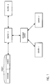
- Figure 1 is a conceptual illustration of packet handling by a router.
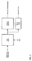
- Figure 2 illustrates one embodiment of a CAM device.
- Figure 3 illustrates one embodiment of a line card or blade of a router having a CAM device configured to perform concurrent lookups.
- Figure 4A illustrates one embodiment of a multiple block CAM device having input string filtering circuits.
- Figure 4B illustrates one embodiment of filtering circuits in a multiple block CAM device.
- Figure 5A illustrates one embodiment of an input string.
- Figure 5B is a conceptual illustration of the operation of CAM device using particular packet header segments from the input string of Figure 5A.
- Figure 6 is a conceptual illustration of one embodiment of the filtering and compacting of an input string.
- Figure 7 is a conceptual illustration of one embodiment of bit manipulation for the filtering and compacting of an input string.
- Figure 8 illustrates one method of programming a filter circuit such that it can filter and compact an input string.
- Figure 9 illustrates one embodiment of cross-bar switch.
- Figure 10 illustrates one embodiment of a memory storage element of the cross-bar switch of Figure 9.
- Figure 11 illustrates one embodiment of a filter circuit.
- Figure 12 illustrates one embodiment of the address generator of Figure 11.
- Figure 13 illustrates another embodiment of the address generator of Figure 11.
- Figure 14 illustrates another embodiment of a filter circuit.
- Figure 15 illustrates one embodiment of a data generator coupled to a block filter register.
- Figure 16 illustrates an example of using the embodiment of Figure 15.
- Figure 17 illustrates ten matrix connections for a cross-bar switch based on the exemplary bit pattern in a block filter register.
- Figure 18 illustrates an alternative embodiment of a data generator coupled to a block filter register.
- Figure 19 illustrates one embodiment of block filter register coupled to a sense amplifier.
- Figure 20 illustrates one embodiment of a cross-bar switch.
- Figure 21 illustrates another embodiment of a filter circuit.
- Figure 22 illustrates one embodiment of the data generator of Figure 21 coupled to OR logic and a block filter register
- Figure 23 illustrates another embodiment of cross-bar switch.
- Embodiments of the present invention include various method steps, which will be described below.
- the steps may be performed by hardware components or may be embodied in machine-executable instructions, which may be used to cause hardware components (e.g., a processor, programming circuit) programmed with the instructions to perform the steps.
- the steps may be performed by a combination of hardware and software.
- Embodiments of the present invention may be provided as a computer program product, or software, that may include a machine-readable medium having stored thereon instructions.
- the machine readable medium may be used to program a computer system (or other electronic devices) to generate articles (e.g., wafer masks) used to manufacture embodiments of the present invention.
- the machine-readable medium may include, but is not limited to, floppy diskettes, optical disks, CD-ROMs, and magneto-optical disks, ROMs, RAMs, EPROMs, EEPROMs, magnet or optical cards, flash memory, or other type of media / machine-readable medium suitable for storing electronic instructions.
- the machine readable medium may store data representing an integrated circuit design layout that includes embodiments of the present invention.
- the design layout for the integrated circuit die may be generated using various means, for examples, schematics, text files, gate-level netlists, hardware description languages, layout files, etc.
- the design layout may be converted into mask layers for fabrication of wafers containing one or more integrated circuit dies.
- the integrated circuit dies may then be assembled into packaged components. Design layout, mask layer generation, and the fabrication and packaging of integrated circuit dies are known in the art; accordingly, a detailed discussion is not provided.
- the method and apparatus described herein provides for the filtering of a common input string to generate one or more filtered comparand strings.
- the filtering of a common input string enables concurrent lookups in different CAM tables to be performed on multiple filtered comparands by different CAM devices (or different blocks of a CAM device), to compare the data in the filtered comparand strings with data stored in its associative memory.
- packet throughput e.g., in a router
- the common input string including multiple comparand or search key information, may be formed by a controller unit such as a network processor or a central processing unit.
- the common input string may include one or more packet headers, or portions thereof.
- the input string may include various routing data in field segments of the input string that may be used to determine the subsequent handling of the packet, for example, Classification, Next Hop, and MAC.
- the same input string is passed through different filter circuits.
- the filter circuits may be preprogrammed to selectively allow one or more segments of the common input string to pass as filtered comparand data to one or more CAM tables.
- the filtering may be performed on a bit basis, where specific predetermined bits are selected from the common input string to generate filtered string segments.
- the filtered string segments may also be shifted to appropriate bit positions to compact the filtered string segments into a compacted filtered comparand string.
- the different compacting and/or filtering operations performed on the input string may be performed in parallel, rather than sequentially, such that a filtering operation may be started before another filtering operation is completed.
- Each of the filtered comparand strings may then be provided to the CAM device blocks. In this manner, all of the CAM device blocks may perform concurrent lookups.
- the filtering and/or compacting may be performed sequentially and be completed before or performed concurrently with subsequent lookups.
- the filtering and compacting operations may be performed by multiple cross-bar switches that are each under the control of a corresponding programming circuit.
- the input string is transmitted in parallel to all of the cross-bar switches.
- Each cross-bar switch may be pre-programmed by its corresponding programming circuit to filter and compact different segments of the input string to generate multiple compacted, filtered comparand strings.
- the multiple, filtered comparand strings can then be used to perform different lookups using different tables.
- the compacted, filtered comparand strings may be continuously filled without any gaps between bits.
- the programming circuit includes, for one example, an address generator, a block filter register, and a data generator.
- the cross-bar switches and/or the block filter registers may be implemented with random access memory (RAM) devices.
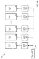
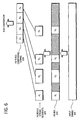
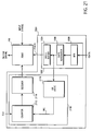
- Figure 3 illustrates one embodiment of a line card or blade of a router having a CAM device configured to perform concurrent lookups.
- Line card 300 includes processor 310, ingress interface circuitry 330, egress interface circuitry 340, CAM device 320, associated data storage unit 370, traffic manager 360, and payload storage unit 350.
- Processor 310 functions to control the overall operation of line card 300 in cooperation with the other components of line card 300. For example, processor 310 receives packets from a network medium through ingress interface circuitry 330, stores the payload of packets in payload storage unit 350, and processes packet header information to determine required lookups in CAM device 320 and subsequent handling of the packets, as discussed herein. Ingress circuitry includes, for example, PHY and MAC devices. Processor 310 sends out packets on a network medium through egress interface circuitry 340 based on the lookups performed by CAM device 320. Egress interface circuitry 340 may be connected to a switch fabric or directly to one or more other routers or switches.
- Processor 310 may be one or more network processor units (NPUs), microprocessors, or one or more special purpose processors such as a digital signal processor (DSP). In another embodiment, processor 310 may be another type of controller, for example, a field programmable gate array or a general purpose processor.
- NPUs network processor units
- DSP digital signal processor
- processor 310 may be another type of controller, for example, a field programmable gate array or a general purpose processor.
- the processor 310, ingress interface circuitry 330, and egress interface circuitry 340 components of a router are known in the art; accordingly, a detailed discussion is not provided.
- processor 310 determines the number and types of lookups to be performed by one or more of CAM devices 320, and forms the search keys for these lookups.
- the searches or lookups may include, for example, Classification lookups, forwarding lookups (e.g., Next Hop or longest prefix match (LPM) lookup, MAC lookup, MPLS lookup, etc.).
- LPM Next Hop or longest prefix match
- processor 310 forms a composite search key that includes at least two, and as many as all, of the various search keys for the lookups.
- the composite search key is provided as a common input string to CAM device 320.
- CAM device 320 selectively identifies and extracts the individual search keys from the common input string and provides the individual search keys to the associated CAM blocks to perform the lookups.
- the lookups can then occur concurrently or simultaneously in the CAM blocks of CAM device 320, thereby increasing overall throughput over conventional systems in which searches are processed sequentially.
- CAM device 320 may be a multiple block CAM device with each block capable of storing a different table for comparand lookups, as discussed below in relation to Figures 4A and 4B.
- CAM device 320 may represent multiple, single block CAM devices (e.g., with each single block CAM device formed on a different integrated circuit substrate) with each CAM device used to store a different table for comparand lookup.
- associated information for matching entries e.g., additional routing information and/or packet information
- Processor 310 then communicates with traffic manager 360 to schedule the exit of a packet from line card 300 via egress interface circuitry 340.
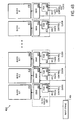
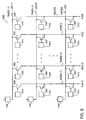
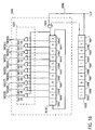
- FIG 4A illustrates one embodiment of a multiple block CAM device having input string filter circuits.
- CAM device 400 may be CAM device 320 of Figure 3. As discussed above in relation to CAM 320 of Figure 3, a block may be an entire array or a portion of a larger array.
- CAM device 400 includes multiple block memory arrays (N blocks) with each block storing a different lookup table or portions of one or more common lookup tables (e.g., block 0 and block 1 may store one lookup table and blocks N-3 to N-1 may store a different lookup table).
- N blocks block memory arrays
- CAM device 400 may have more or less than five blocks.
- Each of blocks 410-414 is coupled to a filter circuit 420-424, respectively.
- Each of filter circuits 420-424 is configured to receive a common input string 405 and filter, extract or remove from input string 405 one or more segments that will be used to perform a lookup.
- CAM device 400 may include multiple, single block CAM devices instead of a single, multiple block CAM device as shown in Figures 4A and 4B.
- Each filter circuit may also compact the extracted search information to form a contiguous bits that participate in a compare with data stored in the corresponding CAM block.
- Each of the filter circuits 420-424 may have dedicated filter functions. Alternatively, each filter circuit may be programmable to dynamically select one or more segments or bits of input string 405.
- each of filter circuits 420-424 includes a cross-bar switch (XBAR) and a programming circuit (PGM).
- filter circuit 420 includes cross-bar switch 430 and programming circuit 440.
- Programming circuit 440 may be used to pre-program cross-bar switch 430 to filter out particular field segments of input string 405 and shift bit positions of the field segments to compact the filtered string segment into a compacted, filtered comparand string.
- one or more of filter circuits 420-424 need not contain a programming circuit.
- one or more of the cross-bar switches may be configured for external device access and direct programming (e.g., by processor 310 of Figure 3). Programming circuits in the CAM device 400 may be included as an added convenience to the user.
- Programming circuit 440 is configured to receive filter data (FDATA), via data line(s) 491, that is used to directly or indirectly program the cross-bar switch 430 to generate a particular filtered comparand string from common input string 405.
- Programming circuit 440 may also be configured to receive one or more control signals via control line(s) 492 and one or more clock signal(s) via line 493 from a clock generator (not shown) to control the operation of the programming circuit, as discussed in detail below.
- filter circuits 421-424 may operate in a manner similar to that discussed for filter circuit 420.
- Each of filter circuits 420-424 may select a different segment, or combination of segments, of the common input string 405 where each block stores a different table.
- one or more filter circuits may select the same segment, or the same combination of segments, of the common input string 405 when, for example, corresponding CAM blocks store portions of the same lookup table.
- each of cross-bar switches 430-434 may be pre-programmed by its corresponding programming circuit 440-444, respectively, to filter appropriate field segments of the input string. All resulting filtered comparand strings may then be concurrently compared with their respective lookup tables stored in the corresponding CAM block. For example, the filtered comparand string generated by filter circuit 420 is compared with the lookup table stored in block 410, while filtered comparand string generated by filter circuit 421 is compared with the lookup table stored in block 411.
- the filtering of common input string 405 to generate the filtered comparand strings or search keys may be accomplished sequentially.
- the lookups in the blocks may also be performed concurrently or sequentially.
- Figure 5A illustrates one embodiment of an input string.
- input string 405 may include field segments parsed or processed from one or more packet headers 510 and 520.
- data processing systems e.g., routers, clients, servers
- the procedure involves the use of protocols by which these systems agree on how to communicate with each other.
- networks may be organized as a series of layers. The number of layers and the function of each layer varies from network to network.
- TCP transmission control protocol
- IP Internet protocol
- TCP packet header 510 includes a source address (SA) port segment 552 and a destination address (DA) port segment 553
- IP packet header 520 includes a SA segment 554, a DA segment 555, a type of service (ToS) segment 551, and a protocol type segment 556.
- SA source address
- DA destination address
- IP packet header 520 includes a SA segment 554, a DA segment 555, a type of service (ToS) segment 551, and a protocol type segment 556.
- processor 310 of Figure 3 may be used to parse certain segments from packet headers 510 and 520 to generate input string 405 and transmit the input string to CAM device 320.
- input string 405 may include MAC segment 557, TOS segment 551, SA port segment 551, DA port segment 552, SA segment 554, and DA segment 555.
- input string 405 may include more or less than the segments illustrated.
- Each of filter circuits (illustrated in Figures 4A and 4B) may then filter out the bit values of different field segments of input string 405 to generate different filtered comparand strings to concurrently perform different lookups in the CAM blocks.
- processor 310 may transmit as-received unparsed header segments to CAM device 320.
- FIG 5B is a conceptual illustration of the operation of CAM device 400 using the packet header segments for input string 405 that are illustrated in Figure 5A.
- CAM device 400 may include three CAM blocks 410, 411, and 412. Each block 410, 411, and 412 is coupled to a corresponding filter circuit 420, 421, and 422, respectively. Each of filter circuits 420-422 is configured to receive input string 405 and process the received input string 405.
- filter circuits 420-422 may be pre-programmed to filter particular field segments of the input string 405 in order to perform concurrent lookups on the various tables stored in blocks 410-412.
- filter circuit 420 may be preprogrammed to filter MAC segment 557 resulting in filtered comparand string 580;
- filter circuit 421 may be preprogrammed to filter DA segment 555 resulting in filtered comparand string 581;
- filter circuit 422 may be preprogrammed to filter SA segment 554, DA field segment 555 and TOS segment 551 resulting in filtered comparand string 582.
- each of filtered comparand strings 580-581 may then be used to concurrently perform the various lookups.
- filtered comparand string 580 may be used to perform a MAC lookup in CAM block 410; filtered comparand string 581 may be used to perform a Next Hop (e.g., LPM) lookup in CAM block 411; and filtered comparand string 582 may be used to perform a Classification lookup in CAM block 412.
- LPM Next Hop
- filtered comparand string 582 may be used to perform a Classification lookup in CAM block 412.
- Figure 6 is a conceptual illustration of one embodiment of the filtering and compacting of an input string.
- input string 405 may be part, or all, of a header of a packet or may include field segments from other parts of a packet or other processed information.
- Input string 405 is passed through a filter 620 that masks out, or blocks, undesired field segments of input string 405.
- the output of filter 620 is one or more filtered string segments 629.
- four string segments X 1 , X 2 , X 3 , and X 4 may be filtered through filter 620.
- the strings segments X 1 , X 2 , X 3 , and X 4 may correspond to, for example, DA, SA, Type of Service (ToS), and protocol type.
- ToS Type of Service
- the filtering of input string 405 may be performed by one or more of filter circuits 420-424, with each of filter circuits 420-424 programmed to filter different field segments of input string 405 or one or more of the same field segments.
- the filtering of input string 405 may be performed on a bit basis. Alternatively, the filtering of input string 405 may be performed based on other sizes, for example, a byte size.
- each of filter circuits 420-424 may be re-programmed to filter different field segments of input string 405 from a prior programmed state.
- the filtered string segments (X 1 , X 2 , X 3 , and X 4 ) 629 may not be adjacent to each other. Such non-adjacent filtered string segments may be shifted to generate a compacted filtered string 639.
- a filter circuit e.g., filter circuit 420 moves the bits of the filtered string segments 629 to generate filtered comparand string 639. In one embodiment, for example, all of the bits of filtered string segment 629 are shifted to the lowest positions. Alternatively, the bits of filtered string segments 629 may be shifted in other manners, for example, to the highest positions.
- Figure 7 is a conceptual illustration of one embodiment of bit manipulation for the filtering and compacting of an input string using a cross-bar switch 720 (e.g., cross-bar switch 430).
- the cross-bar switch 720 includes an n by n matrix of intersections, where n is the bit width of input string 405 and also the bith width of the output string.
- Each of the diamonds (e.g., diamond 721) represents an intersection, and possible connection, for an input bit IN(0)-IN(n-1) and an output bit Y(0)-Y(n-1) of the filtered comparand string.
- cross-bar switch 720 is programmed by program data (PDATA) to select and translate or compact predetermined bits from input string 405 to output bit positions of the compacted filtered comparand string.
- PDATA program data
- the address and/or PDATA may be generated by a program circuit (e.g., program circuit 440 of Figure 4B), or externally (e.g., by processor 310 of Figure 3).
- Line 722 across the diagonal of filter circuit represents a one-to-one connection correlation between the bit positions of an input string 405 and an output filtered comparand string 639.
- the selected or programmed bits pictorially the "+" encapsulated in a circle, (e.g., connection 723 of Figure 7) represent a programmed bit for making a connection between an input bit position and an output bit position.
- Each connection is established by programming one or more circuit elements at the intersections. Programming of an intersection may be accomplished using various means including writing the state of a memory cell, blowing a fuse or other connection, leaving a connection intact, and the like.
- a connection may be established by writing a first logic state (e.g., a logic "1") to the memory element, and no connection may be established by writing a second logic state (e.g., a logic "0") to the memory element.
- a first logic state e.g., a logic "1”
- a second logic state e.g., a logic "0
- Cross-bar switch 720 is programmed to avoid bit gaps in the resulting filtered comparand string 639 that is output by filter circuit 720.
- all of the selected bits of input string 405 are shifted to the lowest bit positions.
- the resulting filtered comparand string 639 may, thus, have significantly fewer bit positions than the input string 405.
- the number of intersections in the cross-bar switch may be reduced to match the number of output bits.
- the lookup entries in each of the CAM blocks 410-414 may be significantly smaller than the size of input string 405.
- a narrower CAM array i.e., having fewer bits per row than the total length of the common input string
- the compacted filtered string may also have desirable power savings as the unused columns of a CAM array may be globally masked by a global mask circuit (not shown) and, thus, draw or dissipate minimal or substantially low power during a search operation.
- Global masks are known in the art; accordingly, a detailed discussion is not provided herein.
- Figure 7 describes a programmed cross-bar switch that compacts or translates input data from higher bit positions to lower bit positions in the output data string.
- Alternative filters may compact or translate input data from lower bit positions to higher bit positions in the output string.
- the filtered string need not be compacted, and the filtered string with gaps, if any, may be provided to a CAM block or table for look-up.
- the unused bits in the search key provided to the CAM block may be globally masked by a global mask register.
- the size of the filtered comparand string generated by cross-bar switch 720 may be smaller than input string 405 even if the selected bits on the input string 405 are contiguous. For example, if the bits of input string 405 to be selected correspond to rows 0 to row 2, the output bits would not need to be shifted, because the selected rows are contiguous. As such, even when the desired bits of input string 405 are contiguous, the size of the resulting filtered comparand string 639 may also be smaller than the size of input string 405 as a whole.
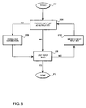
- Figure 8 illustrates one method of programming a filter circuit such that it can filter and compact an input string.
- the method may be performed, for example, by programming circuit 440 of Figure 4B or by processor 310 of Figure 3.
- the method may commence in response to an explicit program instruction or control signal provided to the CAM device, upon reset, or in response to other stimulus.
- gaps in resulting output string 639 may be avoided by continually sequencing through input bits and determining whether the input bit should be provided as a particular output bit.
- step 802. A determination is made at step 804 whether a particular input bit should be provided to a particular output bit position (e.g., as determined by FDATA provided to program circuit 440 of Figure 4B). If so, an appropriate connection is established or programmed in the cross-bar switch at step 806. If this is not the last input bit, step 808, the method moves to the next input bits, step 810, and repeats step 804. When all of the input bits have been processed, the process is complete, step 812.
- Cross-bar switch 1000 that is one embodiment of cross-bar switch 430.
- Cross-bar switch 1000 includes an array of rows and columns of memory storage elements 1010 coupled to the gates of transistors 1020. Each memory storage element/transistor pair is positioned at the intersection of a row and column, and is used to establish (or not establish) a connection between input signals IN(0)-IN(n-1) and output signals Y(0)-Y(n-1).
- Input signals IN represent the input string data (e.g., input string 405 of Figure 4A), and output signals Y represent filtered output string provided to a CAM block or table.
- Each memory storage cell 1010 stores a state that indicates whether a connection is established at a particular row and column intersection in switch 1000.
- the memory storage cells may be any type of memory including, random access memory (RAM) cells (both static and dynamic), read only (ROM) cells, and other volatile or non-volatile memory storage cells.
- RAM random access memory
- ROM read only
- the memory storage cells may be programmed or written to using any write circuitry appropriate for the memory storage cell type. If the memory storage cell stores a logic "1" state, the associated transistor 1020 is enabled to let an input signal IN on one of the signal lines 1030(0)-1030(n-1) to pass to one of the outputs Y on one of the signal lines 1040(0)-1040(n-1).
- the output signal lines 1040 may also be pre-charged to predetermined or default states by precharge circuits 1050.
- Precharge circuits 1050 may be any well-known circuits.
- Cross-bar switch 1000 is a full cross-bar switch that enables any input to be connected to any output Y.
- only a portion of the cross-bar switch 1000 may be needed such as when an input string is compacted.
- the corresponding circuitry of the cross-bar switch for translating lower bit positions to higher bits positions may be removed from a full cross-bar switch.
- the corresponding circuitry of the cross-bar switch for translating higher bit positions to lower significant bits positions may be removed from a full cross-bar switch. Exemplary embodiments of modified cross-bar switches are discussed below.
- FIG. 10 illustrates memory storage cell 1100 that is one embodiment of memory storage cell 1010.
- Cell 1100 includes cross-coupled inverters 1130 and 1140 that form a bi-stable latch for storing data at nodes 1180 and 1190.
- Pass gates 1150 and 1160 allow program data (and read data) to be communicated with the storage nodes when the word line signal on signal line 1110 is active.
- Node 1180 is coupled to the gate of transistor 1020.
- Reset transistor 1170 may also be included to pull node 1180 to a predetermined state of logic "0" when the reset signal Reset on signal line 1120 is activated.
- Reset transistor 1170 has its gate coupled to signal line 1120, its drain coupled to node 1180, and its source coupled to ground.
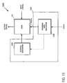
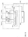
- FIG 11 illustrates filter circuit 1200 that is one embodiment of one of the filter circuits 420-424 of Figure 4A.
- filter circuit 1200 includes a cross-bar matrix switch 430 and a programming circuit 1204.
- a full cross-bar switch e.g., cross-bar switch 1000 of Figure 9
- a full cross-bar switch may be modified to provide only required connection capability, thereby reducing the size of the cross-bar switch.
- programming circuit 1240 includes program data generator 1208 and address generator 1206.
- Program data generator 1208 generates programming data PDATA to program one or more of the intersections of cross-bar switch. PDATA is generated in response to filter data FDATA that indicates which input bits are to be included in the output string, and whether and how the inputs bits are to be compacted or translated in the output string. FDATA may be provided, for example, by processor 310 of Figure 3.
- Address generator 1206 is coupled to cross-bar switch 430. In an alternative embodiment, address generator 1206 may also be coupled to program data generator 1208. Address generator 1206 operates to access one or more intersections of cross-bar switch 430 for programming. Address generator 1206 may include, for example, one or more row and/or column decoders to select one or more rows or columns of intersections in the cross-bar switch for programming, or to select a single intersection or other groups of intersections for programming.
- address generator 1206 includes a decoder 1304 controlled by an address counter 1302 as illustrated in Figure 12.
- Address counter 1302 is configured to sequence decoder 1304 through the rows or columns of cross-bar switch 430 by activating the signals on signal lines 1306(0)-1306(n-1) coupled to the cross-bar switch 430.
- Counter 1302 increments or decrements its count to select a new row or column in response to the clock signal CLK and an enable signal ENABLE that is activated for programming.
- the ENABLE signal may be controlled by program data generator 1208 (e.g., in response to FDATA), or may controlled externally (e.g., by processor 310 of Figure 3).
- address generator 1206 may have other components, for example, a shift register 1402 to sequence through the rows and/or columns of cross-bar switch 430 as shown in Figure 13. Address generators, address decoders, registers, and counters are known in the art; accordingly, a detailed discussion is not provided.
- Figure 14 illustrates program data generator 1502 that is one embodiment of program data generator 1208 of Figure 11.
- Program data generator 1502 includes write buffer circuit 1504, data generator 1506, and block filter register (BFR) 1508.
- Data generator 1506, BFR 1508 and address generator 1206 may optionally receive one or more clock signals CLK as shown as a dashed line in Figure 14.
- Block filter register 1508 stores the particular filter data FDATA that is used to filter input string 405 to obtain a desired filtered comparand string.
- Block filter register 1508 may be programmed (e.g., by processor 310 of Figure 3) with a particular "1" and "0" bit pattern based on the desired filtering of input string 405.
- each of the block filter registers within filter circuits 420-424 may store a different bit pattern in order to filter different bits from the common input string 405 that is applied to all filter circuits 420-424.
- a block filter register may store the same bit pattern as other block filter registers.
- multiple block filter registers may be used in a single program generator 1502 and selectable (e.g., by processor 310 of Figure 3, or by other elements) to provide the appropriate FDATA.
- Block filter register 1508 is coupled to data generator 1506.
- Data generator 1506 generates the PDATA bit pattern that is loaded into write buffer circuit 1504 to selectively program intersections within cross-bar switch 430.
- Write buffer circuit 1504 operates to buffer the data programmed to cross-bar switch 430.
- write buffer circuit 1504 may be part of data generator 1506. Write buffer circuits are known in the art; accordingly, a detailed discussion is not provided.
- FDATA there are as many bits of FDATA loaded into BFR 1508 as there are bits in the input data string.
- a particular bit of FDATA indicates whether the corresponding bit position in the input string will be present in the output string.
- the FDATA in BFR 1508 operates as a mask to filter certain input bits from being provided on the output sting to the CAM block.
- the masking provided by the FDATA allows data generator 1506 to generate the appropriate PDATA for cross-bar switch 430 such that switch 430 will filter and compact the input string appropriately.
- address generator 1206 is configured to initially select a first row of cross-bar switch 430.
- Data generator 1506 programs an interconnection for the selected row and a particular column if the corresponding FDATA bit stored in block filter register 1508 has a "1" stored in the bit position corresponding to that row/column location. If the FDATA bit stored in block filter register 1508 stores a "0" in the bit position corresponding to that row/column location, then data generator 1506 programs a "0" into the row and columns interconnects such that no connections are established for that input row. Address generator 1206 then sequences through the rest of the rows and the additional FDATA bits in the block filter register further determine whether connections are established. For one embodiment, address generator 1206 sequences through the rest of the rows and conditionally sequences through the columns as determined by the FDATA. For another embodiment, address generator 1206 conditionally sequences to a new row and continually sequences through the columns as determined by FDATA.
- Figure 15 illustrates data generator 1606 and BFR 1608 that are embodiments of data generator 1506 and BFR 1508, respectively.
- Data generator 1606 includes shift register 1610, logic circuit 1620, and logic gate 1605.
- Shift register 1610 includes n+1 bits of data wherein the first n bits are initially all logic “0" and the n+1 bit is set to a logic "1".
- Shift register 1610 is a looped shift register such that the "1" preloaded in the n+1 bit position is shifted through the other bit positions of shift register 1610 based on the output of AND gate 1605. As such, at any given time, only one bit position in shift register 1610 contains a logic "1" while the other bit positions contain a logic "0.”
- BFR 1608 is also a shift register and stores n bits of FDATA. Each bit of FDATA stored in BFR 1608 is clocked out to one input of AND gate 1605 by CLK on signal line 1695. AND gate 1605 also receives CLK and, in response to a logic "1" on both FDATA input and CLK, enables shift register 1610 to shift its contents left by one bit. Thus, the FDATA stored in BFR 1608 determines whether shift register 1610 shifts its contents. Note that, shift register 1610 and BFR 1608 may be configured to receive different clock signals. Also note that the output of AND gate 1605 may also be latched or registered prior to signalling to shift register 1610 and logic circuit 1620.
- Each bit in shift register 1610 is also coupled to one input of AND gates 1601(0)-1601(n-1) of logic circuit 1620.
- the other input of the AND gates 1601(0)-1601(n-1) are coupled to receive the output of AND gate 1605.
- CLK is low (i.e., a logic "0" state)
- the AND gates 1601 output a logic "0”.
- CLK is high (i.e., a logic "1” state)
- the AND gates 1601 output the bit contents received from shift register 1610.
- logic circuit 1620 either outputs all "0"s or the bit contents of shift register 1610.
- the signals output from AND gates 1601(0)-1601(n-1) are output to signal lines 1603(0)-1603(n-1), respectively, and are coupled to write buffer circuit 1504 of Figure 14.
- the write buffer circuit 1504 in turn, provides this data as PDATA to the cross-bar switch to establish row and column connections therein.
- logic circuit 1620 either outputs all logic "0"s or the contents of shift register 1610 as the PDATA to program a connection in cross-bar switch 430.
- a row of cross-bar switch 430 is selected by address generator 1206, the row is either programmed with all logic "0"s such that no input bit to output bit location is established, or a single bit for the row is programmed to establish a connection.
- Address generator 1206 then sequences to the next row.
- the PDATA output by logic circuit 1620 is then updated as indicated by the FDATA in BFR 1608. If the next FDATA bit is a logic "0" state, no connection is made for the next row; however, if the next FDATA bit is a logic "1" state, a connection is programmed. In this manner, data generator 1606 and BFR 1608 are able to program cross-bar switch 430 to filter the input string and further compact the string.
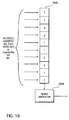
- a specific example is shown in Figure 16.
- BFR 1608 is illustrated with an exemplary bit pattern that may be used to establish certain connections in cross-bar switch 430 to filter and compact bits of input string 405.
- BFR 1608 stores FDATA having a "1" in bit positions 1681,1682,1685,1686,1689 and 1690.
- a "0" is stored in bits positions 1683, 1684, 1687, and 1688.
- address generator 1206 of Figure 14 selects a row (or column) of intersections in cross-bar switch 430 to determine whether the first input bit position IN(0) will be coupled to the corresponding first output bit position Y(0).
- the "1" from bit position 1681 from BFR 1608 is provided to AND gate 1605. Since bit position 1681 has a “1”, on the next clock cycle the "1" in bit position 1650 is shifted into bit position 1640 of shift register 1610.
- AND gates 1601(9)-1601(0) output 0000000001, respectively, as PDATA to the cross-bar switch 430 (via write buffer 1504) to establish a connection between IN(0) and Y(0) at the intersection of column 0 and row 0 of the switch matrix, as illustrated by the "+” in the row 0 and column 0 intersection of Figure 17. Since AND gates 1601(1)-1601(9) output "0"s to other possible interconnections of row zero and other columns, no connections are established for those intersections.
- address generator 1206 selects a second row (row 1) in cross-bar switch 430 to determine whether the second input bit position IN(1) will be coupled to either the first or second output bit positions Y(1) and Y(0), respectively.
- shift register 1610 and logic circuit 1620 On a subsequent clock cycle of CLK, another shift and program operation is performed by shift register 1610 and logic circuit 1620, because BFR 1608 bit position 1682 stores a "1.”
- a "1” is provided to AND gate 1605 and the "1" in bit position 1640 is shifted into bit position 1641 of shift register 1610 and a "0" is shifted into bit position 1640.
- AND gates 1601(9)-1601(0) output 0000000010, respectively, as PDATA to the cross-bar switch 430 (via write buffer 1504) to establish a connection between IN(1) and Y(1) at the intersection of column 1 and row 1 of the switch matrix, as illustrated by the "+” in the row 1 and column 1 intersection of Figure 17. Since AND gates 1601(0) and 1601(2)-1601(9) output "0"s to other possible interconnections of row one and other columns, no connections are established for those intersections.
- Address generator 1206 selects a third row (row 2) in cross-bar switch 430 to determine whether the third input bit position IN(2) will be coupled to either the first, second or third output bit positions Y(0), Y(1) or Y(2), respectively.
- shift register 1610 does not shift due to the "0" stored in bit position 1683 of BFR 1608. As such, no connection is established for row 2 with a column or output of the switch 430. That is, IN(2) is not coupled to a corresponding output bit position in the filter output string and is effectively masked out as shown in Figure 17.
- Address generator 1206 selects a fourth row (row 3) in cross-bar switch 430 to determine whether the fourth input bit position IN(3) will be coupled to either the first, second, third or fourth output bit positions Y(0), Y(1), Y(2), and Y(3), respectively.
- shift register 1610 does not shift due to the "0" stored in bit position 1684 of BFR 1608. As such, no connection is established for row 3 with a column or output of the switch 430. That is, input bit 4 is not coupled to a corresponding output bit position in the filter output string and is effectively masked out as shown in Figure 17.
- Address generator 1206 selects a fifth row (row 4) in cross-bar switch 430 to determine whether the fifth input bit position IN(4) will be coupled to either the first, second, third, fourth or fifth output bit positions Y(0), Y(1), Y(2), Y(3), and Y(4), respectively.
- the "1" in bit position 1641 is shifted into bit position 1642 of shift register 1610.
- AND gates 1601(9)-1601(0) output 0000000100, respectively, as PDATA to the cross-bar switch 430 (via write buffer 1504) to establish a connection between at the intersection of column 2 and row 4 of the switch matrix, as illustrated by the "+" in the row 4 and column 2 intersection of Figure 17.
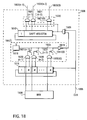
- FIG 18 illustrates data generator 1906 and BFR 1908 that are alternative embodiments of data generator 1506 and BFR 1508 of Figure 15.
- Data generator 1906 includes shift register 1610, logic circuitry 1620 and AND gate 1605 as previously discussed with respect to Figure 15, and additionally includes wired OR circuitry 1913 and shift register 1916.
- Wired OR circuitry 1913 includes an AND gate 1930 and pull-down transistor 1931 pair coupled to receive a different FDATA bit of BFR 1908 and a corresponding bit from shift register 1916.
- BFR 1908 outputs, in parallel, all of its bit position data to wired OR circuitry 1913.
- Wired OR circuitry 1913 controls the shifting operation of shift register 1610.
- wired OR circuitry 1913 is coupled to signal line 1935, which is coupled to a pre-charge (PC) circuit 1918 and the input of inverter 1919.
- PC pre-charge
- the output of inverter 1919 is coupled to an input of AND gate 1905.
- the FDATA stored in BFR 1608 may be complemented and inverter 1919 omitted.
- Shift register 1916 shifts a "1" through its bit positions on each clock of CLK.
- the outputs of AND gates 1930 are coupled to the gates of pull-down transistors 1931 such that signal line 1935 is pulled low and shift register 1610 enabled to shift if the corresponding bit positions in each of BFR 1908 and shift register 1916 are "1"s.
- shift register 1916 and the FDATA stored in BFR 1908 determine which of the data that is input to wired OR circuitry 1913 clocks shift register 1610 on any given clock cycle.
- FIG 19 illustrates that BFR 1508 may be implemented also as a single column random access memory (RAM) 2002 having multiple rows to store the filter mask bit pattern FDATA.
- a desired bit location in the SRAM may be accessed by inputting a decoded row address (e.g., from address generator 1206 of Figure 14).
- a sense amplifier (S/A) 2004 is coupled to the rows of the RAM to output the data value stored at that the accessed bit location.
- the output of sense amplifier 2004 may be coupled, for example, to an input of AND gate 1605.
- RAM 2002 is known in the art; accordingly, a detailed discussion is not provided herein.
- Each of the rows of RAM 2002 may be sequenced using a counter and a decoder such as counter 1302 and decoder 1304 discussed in relation to Figure 12, or by other means, for example, using shift register 1402 of Figure 13.
- cross-bar switch 430 may be a full cross-bar switch (e.g., as shown in Figure 9), or may be modified so as to only use interconnects needed to establish connections.
- FIG 20 shows only four rows and four columns of the modified cross-bar switch, but any number of rows and columns can be used.
- Figure 20 shows that each of the rows of memory storage elements 1010 are coupled to a word line (WL) to enable the elements to communicate data over one or more bit lines represented as D(0)-D(3). Each of the bit lines communicates a bit of the program data PDATA.
- WL word line
- Figure 21 illustrates programming circuit 2004, which is another embodiment of programming circuit 440 of Figure 11.
- programming circuit 2004 includes address generator 2110 and program data generator 1502 of Figure 14.
- Address generator 2110 includes counter 2112, decoder 2114, and OR logic 2116.
- address generator 2110 conditionally sequences through rows of cross-bar switch 430 and programs a connection based on the FDATA stored in BFR 1508. For example, when a particular FDATA bit indicates that a connection is to be established for a selected row in cross-bar switch 430, data generator 1506 outputs at least one signal to write buffer 1504 and OR logic 2116 that has a logic "1" state.
- OR logic 2116 asserts the increment signal INC to an appropriate logic state such that counter 2112 updates its count in response to the clock signal CLK.
- the output of the counter is decoded by decoder 2114 to select a new row in cross-bar switch 430.
- the increment signal may be a decrement signal to decrement counter 2112.
- counter 2112 and decoder 2114 may be replaced by a shift register that is updated to select a row when INC is asserted to the appropriate logic state and CLK is toggled.
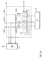
- Figure 22 illustrates data generator 2202 that is one embodiment of data generator 1506 of Figure 21.
- Data generator 2202 includes a shift register 2204 and AND gates 2206(0)-2206(n-1). Each AND gate 2206(0)-2206(n-1) is coupled to receive corresponding bits from shift register 2204 and BFR 1508, and to generate a plurality of PDATA signals on signal lines 2208(0)-2208(n-1). The PDATA signals are provided to write buffer circuitry 1504 and to OR logic 2116.
- a logic "1" state is shifted across the bit positions of shift register 2204 and logically ANDed with corresponding FDATA bits in BFR 1508 by AND gates 2206(0)-2206(n-1).
- the corresponding AND gate 2206 will generate a PDATA signal that will cause the corresponding row and column interconnection in cross-bar switch 430 to be selected and programmed. All other columns for a selected row will be not be programmed or programmed to logic "0" states so as not to establish connections.
- OR logic 2116 will cause the next row to be selected on the next clock cycle to sequence to a new row for programming.
- cross-bar switch 430 may be a full cross-bar switch (e.g., as shown in Figure 9), or may be modified so as to only use interconnects needed to establish connections.
- the data program circuit 1504 illustrated in Figures 21 and 22 that program cross-bar switch 430 to filter and compact input data from higher bit positions to lower bit positions of the output string, only a portion of the cross-bar switch 1000 of Figure 9 may only be needed as shown in Figure 23.
- Figure 23 shows only four rows and four columns of the modified cross-bar switch, but any number of rows and columns can be used.
- Figure 2230 shows that each of the rows of memory storage elements 1010 are coupled to a word line (WL) to enable the elements to communicate data over one or more bit lines represented as D(0)-D(3). Each of the bit lines communicates a bit of the program data PDATA.
- WL word line
Abstract
Description
- This invention relates to the field of memory devices and, in particular, to content addressable memory devices.
- Networks may contain a collection of computing systems (e.g., clients and servers) that are interconnected by transmission lines to enable the transfer of data between them. A network typically includes multiple access points (e.g., routers and servers) that may switch and/or route data between transmission lines to transfer data from a source to a destination. Data is typically transmitted in the form of packets that are made up of smaller data cells. A packet is a unit of data that is routed between a source and a destination on a packet-switched network. When a file (e.g., e-mail, graphics, etc.) is sent from one place to another on a network, the file is divided into such smaller packets making them more efficient for transmission. The individual packets for a given file may travel different routes throughout networks with each packet containing both data and transmission information associated with the routing of data. As such, a packet may be described as having a payload containing the data, and one or more headers that contain the routing information (e.g., a destination address).
- When all the packets have arrived at a destination, they are reassembled into the original file at the receiving end. Such a packet switching scheme is an efficient way to handle transmission on a connectionless network. This is in contrast to a circuit switching scheme where a connection (e.g., a voice connection) requires the dedication of a particular path for the duration of the connection.
- A router is a device (e.g., hardware, firmware, software) that determines the next network segment to which a packet should be forwarded towards its destination. A router may be positioned at points within a network or where one network meets another, referred to as a gateway. A router may create and maintain tables of the available routes and their conditions for use with other information to determine the best route for a given packet. Typically, a packet may travel through a number of network points having routers before arriving at its destination.
- When a data packet arrives at the input of a router, several lookups may be performed to determine the subsequent handling of the packet, as illustrated in Figure 1. The lookups may include, for examples, where to send the packet next (Next Hop), the quality of service requirement (QoS), the Ethernet port address, etc. Consider, for example, a packet arriving at Router-A. Router-A needs to determine whether the packet is destined for local servers connected directly to Router-A, or if the packet should go to the next router on a route (Router-B) to a destination. Additionally, Router-A may assign a priority based on the destination address (DA) and the source address (SA) of the packet.
- The packet header may first be parsed or processed to get the values from different fields (e.g., SA, DA, protocol type, QoS, etc) in order to perform the various lookups. A packet classification lookup, for example, may be performed using SA, DA and other relevant fields in the packet header. The Next Hop lookup, for example, may also be performed to determine whether the packet is meant for local servers or for Router-B. If the packet is destined for Router-B, the packet is then put in a queue for Router-B. If the packet is destined for a local server (e.g., Server-1 or Server-2), then a media access control (MAC) lookup is performed to send the packet to the appropriate server. In the preceding example, three lookups are necessary for sending the packet on its way: Packet Classification, Next Hop, and MAC. However, often there are other lookups performed on the packet header, with the number of lookups exceeding five or more.
- Routers may use processors and content addressable memory (CAM) devices to perform the various lookups on packets. As opposed to a random access memory (RAM) device, in which information is accessed by specifying a particular memory location address, the data stored in a CAM is accessed by the contents of the data. More specifically, instead of using an address to access a particular memory location, a CAM uses a key that contains a portion of the desired contents of a particular memory cell in the memory device. The CAM can be instructed by a processor to compare the key, also referred to as comparand data (e.g., packet header data) with data stored in its associative memory array, as illustrated in Figure 2. The CAM simultaneously examines all of its entries and selects the stored data that matches the key.
- When the entire CAM device, or blocks thereof, is searched - simultaneously for a match of the stored data with the key comparand data, the CAM device indicates the existence of a match by asserting a match flag. Multiple matches may also be indicated by asserting a multiple match flag. The CAM device typically includes a priority encoder to translate the matched location into a match address or CAM index and outputs this address to a status register so that the matched data may be accessed. The priority encoder may also sort out which matching memory location has the top priority if there is more than one matching entry.
- Data may be represented in the form of strings of binary digits ("bits") having a low ("0") logic state and a high ("1") logic state. Different types of CAMs may be used with different data formats. A binary CAM is designed to operate with "0" and "1" states, while a ternary CAM is designed to operate with "0", "1", and "don't care" states. The bits may be organized into groups such as a word (e.g., 64 or 72 bits wide) and stored in different segments of a CAM. The keys used for different data fields may have different word sizes, for example, the key for a Classification lookup may be 128 bits wide and the key for a Next Hop lookup may be 32 bits wide.
- A router may include multiple CAMs, with each CAM having a different table or, alternatively, a single CAM having multiple blocks for each of the different tables, for performing the different lookups. For example, a router may include a 32 bit wide Next Hop CAM, a 128 bit Classification CAM, and a 48 bit MAC CAM. With routers having multiple CAMs, each of the multiple CAMs are typically connected to common buses that are used to communicate the various keys and other input and output data with each of the CAM devices. Similarly, with routers having a single CAM with multiple blocks, each of the blocks is accessed using common buses. Thus, lookups are typically performed sequentially before a packet is processed (e.g., routed to the next destination or classified). Because the buses are shared with so many input and output functions of all the CAMs or CAM blocks, many clock cycles are required to multiplex data on the bus. This generally limits the search rate and overall throughput of conventional CAM devices. As the number of ports, segments, or devices that are supported by routers and as the number of lookups increase, conventional CAM devices and architectures can undesirably limit the system's overall throughput.
- US Patent 6,098,147 is directed to a method and apparatus for longest coincidence data detection using associative memory units having interleaved data. According to this document, each of the N associative memory units compares a distributed portion of external data and a corresponding portion of internal data to a designated bit region from a most significant bit of the distributed portion and outputs a matching signal when the distributed portion of the external data portion and a corresponding portion of the internal data are coincident with each other in the designated bit region. This document also discloses shifting mask bit data if a match is not found in a compare operation, and discloses shifting mask bit data by one bit in the direction of the most significant bit and adding a "0" at the least significant bit thereby keeping bits of the mask data in the same positions relative to each other.
- The present invention as defined in the appended claims pertains to a method and apparatus for concurrent searching of different tables in a content addressable memory array.
- Other features and advantages of the present invention will be apparent from the accompanying drawings, and from the detailed description, which follows below.
- The present invention is illustrated by way of example and not intended to be limited by the figures of the accompanying drawings.
- Figure 1 is a conceptual illustration of packet handling by a router.
- Figure 2 illustrates one embodiment of a CAM device.
- Figure 3 illustrates one embodiment of a line card or blade of a router having a CAM device configured to perform concurrent lookups.
- Figure 4A illustrates one embodiment of a multiple block CAM device having input string filtering circuits.
- Figure 4B illustrates one embodiment of filtering circuits in a multiple block CAM device.
- Figure 5A illustrates one embodiment of an input string.
- Figure 5B is a conceptual illustration of the operation of CAM device using particular packet header segments from the input string of Figure 5A.
- Figure 6 is a conceptual illustration of one embodiment of the filtering and compacting of an input string.
- Figure 7 is a conceptual illustration of one embodiment of bit manipulation for the filtering and compacting of an input string.
- Figure 8 illustrates one method of programming a filter circuit such that it can filter and compact an input string.
- Figure 9 illustrates one embodiment of cross-bar switch.
- Figure 10 illustrates one embodiment of a memory storage element of the cross-bar switch of Figure 9.
- Figure 11 illustrates one embodiment of a filter circuit.
- Figure 12 illustrates one embodiment of the address generator of Figure 11.
- Figure 13 illustrates another embodiment of the address generator of Figure 11.
- Figure 14 illustrates another embodiment of a filter circuit.
- Figure 15 illustrates one embodiment of a data generator coupled to a block filter register.
- Figure 16 illustrates an example of using the embodiment of Figure 15.
- Figure 17 illustrates ten matrix connections for a cross-bar switch based on the exemplary bit pattern in a block filter register.
- Figure 18 illustrates an alternative embodiment of a data generator coupled to a block filter register.
- Figure 19 illustrates one embodiment of block filter register coupled to a sense amplifier.
- Figure 20 illustrates one embodiment of a cross-bar switch.
- Figure 21 illustrates another embodiment of a filter circuit.
- Figure 22 illustrates one embodiment of the data generator of Figure 21 coupled to OR logic and a block filter register
- Figure 23 illustrates another embodiment of cross-bar switch.
- In the following description, numerous specific details are set forth such as examples of specific, components, circuits, processes, etc. in order to provide a thorough understanding of the present invention. It will be apparent, however, to one skilled in the art that these specific details need not be employed to practice the present invention. In other instances, well known components or methods have not been described in detail in order to avoid unnecessarily obscuring the present invention.
- Embodiments of the present invention include various method steps, which will be described below. The steps may be performed by hardware components or may be embodied in machine-executable instructions, which may be used to cause hardware components (e.g., a processor, programming circuit) programmed with the instructions to perform the steps. Alternatively, the steps may be performed by a combination of hardware and software.
- Embodiments of the present invention may be provided as a computer program product, or software, that may include a machine-readable medium having stored thereon instructions. The machine readable medium may be used to program a computer system (or other electronic devices) to generate articles (e.g., wafer masks) used to manufacture embodiments of the present invention. The machine-readable medium may include, but is not limited to, floppy diskettes, optical disks, CD-ROMs, and magneto-optical disks, ROMs, RAMs, EPROMs, EEPROMs, magnet or optical cards, flash memory, or other type of media / machine-readable medium suitable for storing electronic instructions.
- The machine readable medium may store data representing an integrated circuit design layout that includes embodiments of the present invention. The design layout for the integrated circuit die may be generated using various means, for examples, schematics, text files, gate-level netlists, hardware description languages, layout files, etc. The design layout may be converted into mask layers for fabrication of wafers containing one or more integrated circuit dies. The integrated circuit dies may then be assembled into packaged components. Design layout, mask layer generation, and the fabrication and packaging of integrated circuit dies are known in the art; accordingly, a detailed discussion is not provided.
- The method and apparatus described herein provides for the filtering of a common input string to generate one or more filtered comparand strings. In one embodiment, the filtering of a common input string enables concurrent lookups in different CAM tables to be performed on multiple filtered comparands by different CAM devices (or different blocks of a CAM device), to compare the data in the filtered comparand strings with data stored in its associative memory. By performing multiple lookups in parallel, rather than sequentially, packet throughput (e.g., in a router) may be significantly increased.
- The common input string, including multiple comparand or search key information, may be formed by a controller unit such as a network processor or a central processing unit. In one embodiment, the common input string may include one or more packet headers, or portions thereof. The input string may include various routing data in field segments of the input string that may be used to determine the subsequent handling of the packet, for example, Classification, Next Hop, and MAC. The same input string is passed through different filter circuits. The filter circuits may be preprogrammed to selectively allow one or more segments of the common input string to pass as filtered comparand data to one or more CAM tables.
- In one embodiment, the filtering may be performed on a bit basis, where specific predetermined bits are selected from the common input string to generate filtered string segments. The filtered string segments may also be shifted to appropriate bit positions to compact the filtered string segments into a compacted filtered comparand string. The different compacting and/or filtering operations performed on the input string may be performed in parallel, rather than sequentially, such that a filtering operation may be started before another filtering operation is completed. Each of the filtered comparand strings may then be provided to the CAM device blocks. In this manner, all of the CAM device blocks may perform concurrent lookups. Alternatively, the filtering and/or compacting may be performed sequentially and be completed before or performed concurrently with subsequent lookups.
- In one embodiment, the filtering and compacting operations may be performed by multiple cross-bar switches that are each under the control of a corresponding programming circuit. The input string is transmitted in parallel to all of the cross-bar switches. Each cross-bar switch may be pre-programmed by its corresponding programming circuit to filter and compact different segments of the input string to generate multiple compacted, filtered comparand strings. The multiple, filtered comparand strings can then be used to perform different lookups using different tables. The compacted, filtered comparand strings may be continuously filled without any gaps between bits. The programming circuit includes, for one example, an address generator, a block filter register, and a data generator. In one embodiment, the cross-bar switches and/or the block filter registers may be implemented with random access memory (RAM) devices.
- Figure 3 illustrates one embodiment of a line card or blade of a router having a CAM device configured to perform concurrent lookups.
Line card 300 includesprocessor 310,ingress interface circuitry 330,egress interface circuitry 340,CAM device 320, associateddata storage unit 370,traffic manager 360, and payload storage unit 350. -
Processor 310 functions to control the overall operation ofline card 300 in cooperation with the other components ofline card 300. For example,processor 310 receives packets from a network medium throughingress interface circuitry 330, stores the payload of packets in payload storage unit 350, and processes packet header information to determine required lookups inCAM device 320 and subsequent handling of the packets, as discussed herein. Ingress circuitry includes, for example, PHY and MAC devices.Processor 310 sends out packets on a network medium throughegress interface circuitry 340 based on the lookups performed byCAM device 320.Egress interface circuitry 340 may be connected to a switch fabric or directly to one or more other routers or switches.Processor 310 may be one or more network processor units (NPUs), microprocessors, or one or more special purpose processors such as a digital signal processor (DSP). In another embodiment,processor 310 may be another type of controller, for example, a field programmable gate array or a general purpose processor. Theprocessor 310,ingress interface circuitry 330, andegress interface circuitry 340 components of a router are known in the art; accordingly, a detailed discussion is not provided. - In response to information in a packet header, for a particular packet,
processor 310 determines the number and types of lookups to be performed by one or more ofCAM devices 320, and forms the search keys for these lookups. The searches or lookups may include, for example, Classification lookups, forwarding lookups (e.g., Next Hop or longest prefix match (LPM) lookup, MAC lookup, MPLS lookup, etc.). When multiple searches are required,processor 310 forms a composite search key that includes at least two, and as many as all, of the various search keys for the lookups. The composite search key is provided as a common input string toCAM device 320.CAM device 320 selectively identifies and extracts the individual search keys from the common input string and provides the individual search keys to the associated CAM blocks to perform the lookups. Advantageously, the lookups can then occur concurrently or simultaneously in the CAM blocks ofCAM device 320, thereby increasing overall throughput over conventional systems in which searches are processed sequentially. -
CAM device 320 may be a multiple block CAM device with each block capable of storing a different table for comparand lookups, as discussed below in relation to Figures 4A and 4B. Alternatively,CAM device 320 may represent multiple, single block CAM devices (e.g., with each single block CAM device formed on a different integrated circuit substrate) with each CAM device used to store a different table for comparand lookup. After one or more lookups are executed inCAM device 320, associated information for matching entries (e.g., additional routing information and/or packet information) may be retrieved from associateddata unit 370.Processor 310 then communicates withtraffic manager 360 to schedule the exit of a packet fromline card 300 viaegress interface circuitry 340. - Figure 4A illustrates one embodiment of a multiple block CAM device having input string filter circuits.
CAM device 400 may beCAM device 320 of Figure 3. As discussed above in relation toCAM 320 of Figure 3, a block may be an entire array or a portion of a larger array. In one embodiment,CAM device 400 includes multiple block memory arrays (N blocks) with each block storing a different lookup table or portions of one or more common lookup tables (e.g., block 0 andblock 1 may store one lookup table and blocks N-3 to N-1 may store a different lookup table). Although five blocks 410-414 are shown for ease of illustration,CAM device 400 may have more or less than five blocks. Each of blocks 410-414 is coupled to a filter circuit 420-424, respectively. Each of filter circuits 420-424 is configured to receive acommon input string 405 and filter, extract or remove frominput string 405 one or more segments that will be used to perform a lookup. In an alternative embodiment,CAM device 400 may include multiple, single block CAM devices instead of a single, multiple block CAM device as shown in Figures 4A and 4B. Each filter circuit may also compact the extracted search information to form a contiguous bits that participate in a compare with data stored in the corresponding CAM block. - Each of the filter circuits 420-424 may have dedicated filter functions. Alternatively, each filter circuit may be programmable to dynamically select one or more segments or bits of
input string 405. - In one embodiment, illustrated in Figure 4B, each of filter circuits 420-424 includes a cross-bar switch (XBAR) and a programming circuit (PGM). For example,
filter circuit 420 includescross-bar switch 430 andprogramming circuit 440.Programming circuit 440 may be used to pre-programcross-bar switch 430 to filter out particular field segments ofinput string 405 and shift bit positions of the field segments to compact the filtered string segment into a compacted, filtered comparand string. It should be noted that one or more of filter circuits 420-424 need not contain a programming circuit. For example, one or more of the cross-bar switches may be configured for external device access and direct programming (e.g., byprocessor 310 of Figure 3). Programming circuits in theCAM device 400 may be included as an added convenience to the user. -
Programming circuit 440 is configured to receive filter data (FDATA), via data line(s) 491, that is used to directly or indirectly program thecross-bar switch 430 to generate a particular filtered comparand string fromcommon input string 405.Programming circuit 440 may also be configured to receive one or more control signals via control line(s) 492 and one or more clock signal(s) vialine 493 from a clock generator (not shown) to control the operation of the programming circuit, as discussed in detail below. - It should be noted that filter circuits 421-424 may operate in a manner similar to that discussed for
filter circuit 420. Each of filter circuits 420-424 may select a different segment, or combination of segments, of thecommon input string 405 where each block stores a different table. Alternatively, one or more filter circuits may select the same segment, or the same combination of segments, of thecommon input string 405 when, for example, corresponding CAM blocks store portions of the same lookup table. As such, each of cross-bar switches 430-434 may be pre-programmed by its corresponding programming circuit 440-444, respectively, to filter appropriate field segments of the input string. All resulting filtered comparand strings may then be concurrently compared with their respective lookup tables stored in the corresponding CAM block. For example, the filtered comparand string generated byfilter circuit 420 is compared with the lookup table stored inblock 410, while filtered comparand string generated byfilter circuit 421 is compared with the lookup table stored inblock 411. - In an alternative embodiment, the filtering of
common input string 405 to generate the filtered comparand strings or search keys may be accomplished sequentially. The lookups in the blocks may also be performed concurrently or sequentially. - Figure 5A illustrates one embodiment of an input string. In one embodiment,
input string 405 may include field segments parsed or processed from one ormore packet headers - For example, where a transmission control protocol (TCP)/Internet protocol (IP) is used, it is organized into multiple layers including a network access layer and an Internet layer. The network access layer uses a TCP to enable the exchange of data between an end system and a network. An Internet layer uses an IP to enable data to transverse multiple interconnected networks. Each of these protocols use packet headers containing routing information, as discussed above. For example,
TCP packet header 510 includes a source address (SA)port segment 552 and a destination address (DA)port segment 553, andIP packet header 520 includes aSA segment 554, aDA segment 555, a type of service (ToS)segment 551, and aprotocol type segment 556. - In one embodiment, for example,
processor 310 of Figure 3 may be used to parse certain segments frompacket headers input string 405 and transmit the input string toCAM device 320. For example,input string 405 may includeMAC segment 557,TOS segment 551,SA port segment 551, DAport segment 552,SA segment 554, andDA segment 555. Alternatively,input string 405 may include more or less than the segments illustrated. Each of filter circuits (illustrated in Figures 4A and 4B) may then filter out the bit values of different field segments ofinput string 405 to generate different filtered comparand strings to concurrently perform different lookups in the CAM blocks. In an alternative embodiment,processor 310 may transmit as-received unparsed header segments toCAM device 320. - Figure 5B is a conceptual illustration of the operation of
CAM device 400 using the packet header segments forinput string 405 that are illustrated in Figure 5A. For example,CAM device 400 may include threeCAM blocks block corresponding filter circuit input string 405 and process the receivedinput string 405. - In one embodiment, filter circuits 420-422 may be pre-programmed to filter particular field segments of the
input string 405 in order to perform concurrent lookups on the various tables stored in blocks 410-412. For example:filter circuit 420 may be preprogrammed to filterMAC segment 557 resulting in filteredcomparand string 580;filter circuit 421 may be preprogrammed to filter DAsegment 555 resulting in filteredcomparand string 581; andfilter circuit 422 may be preprogrammed to filterSA segment 554,DA field segment 555 andTOS segment 551 resulting in filteredcomparand string 582. By filtering different field segments from acommon input string 405, in parallel, each of filtered comparand strings 580-581 may then be used to concurrently perform the various lookups. For example: filteredcomparand string 580 may be used to perform a MAC lookup inCAM block 410; filteredcomparand string 581 may be used to perform a Next Hop (e.g., LPM) lookup inCAM block 411; and filteredcomparand string 582 may be used to perform a Classification lookup inCAM block 412. As such, if each lookup individually requires X clock cycles to perform, only a total of X clock cycles may be required to perform all three lookups because the lookups are performed concurrently. In this manner, packet throughput in a router may be significantly increased over routers utilizing prior CAM architectures. - Figure 6 is a conceptual illustration of one embodiment of the filtering and compacting of an input string. As previously discussed,
input string 405 may be part, or all, of a header of a packet or may include field segments from other parts of a packet or other processed information.Input string 405 is passed through afilter 620 that masks out, or blocks, undesired field segments ofinput string 405. The output offilter 620 is one or morefiltered string segments 629. For example, four string segments X1, X2, X3, and X4 may be filtered throughfilter 620. The strings segments X1, X2, X3, and X4 may correspond to, for example, DA, SA, Type of Service (ToS), and protocol type. The filtering ofinput string 405 may be performed by one or more of filter circuits 420-424, with each of filter circuits 420-424 programmed to filter different field segments ofinput string 405 or one or more of the same field segments. The filtering ofinput string 405 may be performed on a bit basis. Alternatively, the filtering ofinput string 405 may be performed based on other sizes, for example, a byte size. Moreover, each of filter circuits 420-424 may be re-programmed to filter different field segments ofinput string 405 from a prior programmed state. - As shown in Figure 6, the filtered string segments (X1, X2, X3, and X4) 629 may not be adjacent to each other. Such non-adjacent filtered string segments may be shifted to generate a compacted filtered
string 639. Where the filtering is performed, for example, on a bit basis, a filter circuit (e.g., filter circuit 420) moves the bits of the filteredstring segments 629 to generate filteredcomparand string 639. In one embodiment, for example, all of the bits of filteredstring segment 629 are shifted to the lowest positions.
Alternatively, the bits of filteredstring segments 629 may be shifted in other manners, for example, to the highest positions. - Figure 7 is a conceptual illustration of one embodiment of bit manipulation for the filtering and compacting of an input string using a cross-bar switch 720 (e.g., cross-bar switch 430). The
cross-bar switch 720 includes an n by n matrix of intersections, where n is the bit width ofinput string 405 and also the bith width of the output string. Each of the diamonds (e.g., diamond 721) represents an intersection, and possible connection, for an input bit IN(0)-IN(n-1) and an output bit Y(0)-Y(n-1) of the filtered comparand string. One or more intersections is selected by an address, andcross-bar switch 720 is programmed by program data (PDATA) to select and translate or compact predetermined bits frominput string 405 to output bit positions of the compacted filtered comparand string. The address and/or PDATA may be generated by a program circuit (e.g.,program circuit 440 of Figure 4B), or externally (e.g., byprocessor 310 of Figure 3). -
Line 722 across the diagonal of filter circuit represents a one-to-one connection correlation between the bit positions of aninput string 405 and an output filteredcomparand string 639. The selected or programmed bits, pictorially the "+" encapsulated in a circle, (e.g.,connection 723 of Figure 7) represent a programmed bit for making a connection between an input bit position and an output bit position. Each connection is established by programming one or more circuit elements at the intersections. Programming of an intersection may be accomplished using various means including writing the state of a memory cell, blowing a fuse or other connection, leaving a connection intact, and the like. For example, when a memory element is used to establish connections at an intersection, a connection may be established by writing a first logic state (e.g., a logic "1") to the memory element, and no connection may be established by writing a second logic state (e.g., a logic "0") to the memory element. -
Cross-bar switch 720 is programmed to avoid bit gaps in the resulting filteredcomparand string 639 that is output byfilter circuit 720. In the illustrated example, all of the selected bits ofinput string 405 are shifted to the lowest bit positions. The resulting filteredcomparand string 639 may, thus, have significantly fewer bit positions than theinput string 405. For example, theinput string 405 may be 288 bits wide (n= 288), whereas the filteredcomparand string 639 may be only 72 or 144 bits wide. The number of intersections in the cross-bar switch may be reduced to match the number of output bits. Advantageously, the lookup entries in each of the CAM blocks 410-414 may be significantly smaller than the size ofinput string 405. Thus, a narrower CAM array (i.e., having fewer bits per row than the total length of the common input string) may be used. The compacted filtered string may also have desirable power savings as the unused columns of a CAM array may be globally masked by a global mask circuit (not shown) and, thus, draw or dissipate minimal or substantially low power during a search operation. Global masks are known in the art; accordingly, a detailed discussion is not provided herein. - The illustration of Figure 7 describes a programmed cross-bar switch that compacts or translates input data from higher bit positions to lower bit positions in the output data string. Alternative filters may compact or translate input data from lower bit positions to higher bit positions in the output string. Additionally, the filtered string need not be compacted, and the filtered string with gaps, if any, may be provided to a CAM block or table for look-up. The unused bits in the search key provided to the CAM block may be globally masked by a global mask register.
- It should be noted that the size of the filtered comparand string generated by
cross-bar switch 720 may be smaller thaninput string 405 even if the selected bits on theinput string 405 are contiguous. For example, if the bits ofinput string 405 to be selected correspond torows 0 torow 2, the output bits would not need to be shifted, because the selected rows are contiguous. As such, even when the desired bits ofinput string 405 are contiguous, the size of the resulting filteredcomparand string 639 may also be smaller than the size ofinput string 405 as a whole. - Figure 8 illustrates one method of programming a filter circuit such that it can filter and compact an input string. The method may be performed, for example, by
programming circuit 440 of Figure 4B or byprocessor 310 of Figure 3. The method may commence in response to an explicit program instruction or control signal provided to the CAM device, upon reset, or in response to other stimulus. In one embodiment, gaps in resultingoutput string 639 may be avoided by continually sequencing through input bits and determining whether the input bit should be provided as a particular output bit. - Programming starts at
step 802. A determination is made atstep 804 whether a particular input bit should be provided to a particular output bit position (e.g., as determined by FDATA provided toprogram circuit 440 of Figure 4B). If so, an appropriate connection is established or programmed in the cross-bar switch atstep 806. If this is not the last input bit,step 808, the method moves to the next input bits,step 810, and repeatsstep 804. When all of the input bits have been processed, the process is complete,step 812. - Any type of cross bar switch may be used for
cross-bar switch 430 of Figure 4. Figure 9 illustratescross-bar switch 1000 that is one embodiment ofcross-bar switch 430.Cross-bar switch 1000 includes an array of rows and columns ofmemory storage elements 1010 coupled to the gates oftransistors 1020. Each memory storage element/transistor pair is positioned at the intersection of a row and column, and is used to establish (or not establish) a connection between input signals IN(0)-IN(n-1) and output signals Y(0)-Y(n-1). Input signals IN represent the input string data (e.g.,input string 405 of Figure 4A), and output signals Y represent filtered output string provided to a CAM block or table. - Each
memory storage cell 1010 stores a state that indicates whether a connection is established at a particular row and column intersection inswitch 1000. The memory storage cells may be any type of memory including, random access memory (RAM) cells (both static and dynamic), read only (ROM) cells, and other volatile or non-volatile memory storage cells. The memory storage cells may be programmed or written to using any write circuitry appropriate for the memory storage cell type. If the memory storage cell stores a logic "1" state, the associatedtransistor 1020 is enabled to let an input signal IN on one of the signal lines 1030(0)-1030(n-1) to pass to one of the outputs Y on one of the signal lines 1040(0)-1040(n-1). Theoutput signal lines 1040 may also be pre-charged to predetermined or default states byprecharge circuits 1050.Precharge circuits 1050 may be any well-known circuits. -
Cross-bar switch 1000 is a full cross-bar switch that enables any input to be connected to any output Y. For alternative embodiments, only a portion of thecross-bar switch 1000 may be needed such as when an input string is compacted. For example, when compacting the input string from higher bit positions to lower bit positions in the output string, the corresponding circuitry of the cross-bar switch for translating lower bit positions to higher bits positions may be removed from a full cross-bar switch. Similarly, when compacting the input string from lower bit positions to higher significant bit positions in the output string, the corresponding circuitry of the cross-bar switch for translating higher bit positions to lower significant bits positions may be removed from a full cross-bar switch. Exemplary embodiments of modified cross-bar switches are discussed below. - Figure 10 illustrates
memory storage cell 1100 that is one embodiment ofmemory storage cell 1010.Cell 1100 includescross-coupled inverters nodes gates signal line 1110 is active.Node 1180 is coupled to the gate oftransistor 1020.Reset transistor 1170 may also be included to pullnode 1180 to a predetermined state of logic "0" when the reset signal Reset onsignal line 1120 is activated.Reset transistor 1170 has its gate coupled to signalline 1120, its drain coupled tonode 1180, and its source coupled to ground. - Figure 11 illustrates
filter circuit 1200 that is one embodiment of one of the filter circuits 420-424 of Figure 4A. In this embodiment,filter circuit 1200 includes across-bar matrix switch 430 and aprogramming circuit 1204. In one embodiment, a full cross-bar switch (e.g.,cross-bar switch 1000 of Figure 9) may be used forcross-bar switch 430. In an alternative embodiment, a full cross-bar switch may be modified to provide only required connection capability, thereby reducing the size of the cross-bar switch. - In this embodiment, programming circuit 1240 includes
program data generator 1208 andaddress generator 1206.Program data generator 1208 generates programming data PDATA to program one or more of the intersections of cross-bar switch. PDATA is generated in response to filter data FDATA that indicates which input bits are to be included in the output string, and whether and how the inputs bits are to be compacted or translated in the output string. FDATA may be provided, for example, byprocessor 310 of Figure 3.Address generator 1206 is coupled tocross-bar switch 430. In an alternative embodiment,address generator 1206 may also be coupled toprogram data generator 1208.Address generator 1206 operates to access one or more intersections ofcross-bar switch 430 for programming.Address generator 1206 may include, for example, one or more row and/or column decoders to select one or more rows or columns of intersections in the cross-bar switch for programming, or to select a single intersection or other groups of intersections for programming. - In one embodiment,
address generator 1206 includes adecoder 1304 controlled by anaddress counter 1302 as illustrated in Figure 12.Address counter 1302 is configured to sequencedecoder 1304 through the rows or columns ofcross-bar switch 430 by activating the signals on signal lines 1306(0)-1306(n-1) coupled to thecross-bar switch 430.Counter 1302 increments or decrements its count to select a new row or column in response to the clock signal CLK and an enable signal ENABLE that is activated for programming. The ENABLE signal may be controlled by program data generator 1208 (e.g., in response to FDATA), or may controlled externally (e.g., byprocessor 310 of Figure 3). Alternatively,address generator 1206 may have other components, for example, ashift register 1402 to sequence through the rows and/or columns ofcross-bar switch 430 as shown in Figure 13. Address generators, address decoders, registers, and counters are known in the art; accordingly, a detailed discussion is not provided. - Figure 14 illustrates
program data generator 1502 that is one embodiment ofprogram data generator 1208 of Figure 11.Program data generator 1502 includeswrite buffer circuit 1504,data generator 1506, and block filter register (BFR) 1508.Data generator 1506,BFR 1508 andaddress generator 1206 may optionally receive one or more clock signals CLK as shown as a dashed line in Figure 14. - Block filter register 1508 stores the particular filter data FDATA that is used to filter
input string 405 to obtain a desired filtered comparand string.Block filter register 1508 may be programmed (e.g., byprocessor 310 of Figure 3) with a particular "1" and "0" bit pattern based on the desired filtering ofinput string 405. As such, each of the block filter registers within filter circuits 420-424 may store a different bit pattern in order to filter different bits from thecommon input string 405 that is applied to all filter circuits 420-424. Alternatively, a block filter register may store the same bit pattern as other block filter registers. In another embodiment, multiple block filter registers may be used in asingle program generator 1502 and selectable (e.g., byprocessor 310 of Figure 3, or by other elements) to provide the appropriate FDATA. -
Block filter register 1508 is coupled todata generator 1506.Data generator 1506 generates the PDATA bit pattern that is loaded intowrite buffer circuit 1504 to selectively program intersections withincross-bar switch 430. Writebuffer circuit 1504 operates to buffer the data programmed tocross-bar switch 430. In one embodiment, writebuffer circuit 1504 may be part ofdata generator 1506. Write buffer circuits are known in the art; accordingly, a detailed discussion is not provided. - For one embodiment, there are as many bits of FDATA loaded into
BFR 1508 as there are bits in the input data string. A particular bit of FDATA indicates whether the corresponding bit position in the input string will be present in the output string. In this manner, the FDATA inBFR 1508 operates as a mask to filter certain input bits from being provided on the output sting to the CAM block. The masking provided by the FDATA allowsdata generator 1506 to generate the appropriate PDATA forcross-bar switch 430 such thatswitch 430 will filter and compact the input string appropriately. - In one exemplary illustration of the operation of
program circuit 1204,address generator 1206 is configured to initially select a first row ofcross-bar switch 430.Data generator 1506 programs an interconnection for the selected row and a particular column if the corresponding FDATA bit stored inblock filter register 1508 has a "1" stored in the bit position corresponding to that row/column location. If the FDATA bit stored inblock filter register 1508 stores a "0" in the bit position corresponding to that row/column location, thendata generator 1506 programs a "0" into the row and columns interconnects such that no connections are established for that input row.Address generator 1206 then sequences through the rest of the rows and the additional FDATA bits in the block filter register further determine whether connections are established. For one embodiment,address generator 1206 sequences through the rest of the rows and conditionally sequences through the columns as determined by the FDATA. For another embodiment,address generator 1206 conditionally sequences to a new row and continually sequences through the columns as determined by FDATA. - Figure 15 illustrates
data generator 1606 andBFR 1608 that are embodiments ofdata generator 1506 andBFR 1508, respectively.Data generator 1606 includesshift register 1610,logic circuit 1620, andlogic gate 1605.Shift register 1610 includes n+1 bits of data wherein the first n bits are initially all logic "0" and the n+1 bit is set to a logic "1".Shift register 1610 is a looped shift register such that the "1" preloaded in the n+1 bit position is shifted through the other bit positions ofshift register 1610 based on the output of ANDgate 1605. As such, at any given time, only one bit position inshift register 1610 contains a logic "1" while the other bit positions contain a logic "0." -
BFR 1608 is also a shift register and stores n bits of FDATA. Each bit of FDATA stored inBFR 1608 is clocked out to one input of ANDgate 1605 by CLK onsignal line 1695. ANDgate 1605 also receives CLK and, in response to a logic "1" on both FDATA input and CLK, enablesshift register 1610 to shift its contents left by one bit. Thus, the FDATA stored inBFR 1608 determines whethershift register 1610 shifts its contents. Note that,shift register 1610 andBFR 1608 may be configured to receive different clock signals. Also note that the output of ANDgate 1605 may also be latched or registered prior to signalling toshift register 1610 andlogic circuit 1620. - Each bit in
shift register 1610 is also coupled to one input of AND gates 1601(0)-1601(n-1) oflogic circuit 1620. The other input of the AND gates 1601(0)-1601(n-1) are coupled to receive the output of ANDgate 1605. When CLK is low (i.e., a logic "0" state), the ANDgates 1601 output a logic "0". When CLK is high (i.e., a logic "1" state), the ANDgates 1601 output the bit contents received fromshift register 1610. With such a configuration,logic circuit 1620 either outputs all "0"s or the bit contents ofshift register 1610. The signals output from AND gates 1601(0)-1601(n-1) are output to signal lines 1603(0)-1603(n-1), respectively, and are coupled to writebuffer circuit 1504 of Figure 14. Thewrite buffer circuit 1504, in turn, provides this data as PDATA to the cross-bar switch to establish row and column connections therein. - As noted above,
logic circuit 1620 either outputs all logic "0"s or the contents ofshift register 1610 as the PDATA to program a connection incross-bar switch 430. When a row ofcross-bar switch 430 is selected byaddress generator 1206, the row is either programmed with all logic "0"s such that no input bit to output bit location is established, or a single bit for the row is programmed to establish a connection.Address generator 1206 then sequences to the next row. The PDATA output bylogic circuit 1620 is then updated as indicated by the FDATA inBFR 1608. If the next FDATA bit is a logic "0" state, no connection is made for the next row; however, if the next FDATA bit is a logic "1" state, a connection is programmed. In this manner,data generator 1606 andBFR 1608 are able to programcross-bar switch 430 to filter the input string and further compact the string. A specific example is shown in Figure 16. - In Figure 16,
shift register 1610 has 11 bit positions (n=10) andBFR 1608 has ten bit positions.BFR 1608 is illustrated with an exemplary bit pattern that may be used to establish certain connections incross-bar switch 430 to filter and compact bits ofinput string 405. In this example,BFR 1608 stores FDATA having a "1" inbit positions input string 405, a "0" is stored inbits positions - Initially,
address generator 1206 of Figure 14 selects a row (or column) of intersections incross-bar switch 430 to determine whether the first input bit position IN(0) will be coupled to the corresponding first output bit position Y(0). In the first clock cycle of CLK, the "1" frombit position 1681 fromBFR 1608 is provided to ANDgate 1605. Sincebit position 1681 has a "1", on the next clock cycle the "1" inbit position 1650 is shifted intobit position 1640 ofshift register 1610. Subsequently, AND gates 1601(9)-1601(0) output 0000000001, respectively, as PDATA to the cross-bar switch 430 (via write buffer 1504) to establish a connection between IN(0) and Y(0) at the intersection ofcolumn 0 androw 0 of the switch matrix, as illustrated by the "+" in therow 0 andcolumn 0 intersection of Figure 17. Since AND gates 1601(1)-1601(9) output "0"s to other possible interconnections of row zero and other columns, no connections are established for those intersections. - Subsequently,
address generator 1206 selects a second row (row 1) incross-bar switch 430 to determine whether the second input bit position IN(1) will be coupled to either the first or second output bit positions Y(1) and Y(0), respectively. On a subsequent clock cycle of CLK, another shift and program operation is performed byshift register 1610 andlogic circuit 1620, becauseBFR 1608bit position 1682 stores a "1." A "1" is provided to ANDgate 1605 and the "1" inbit position 1640 is shifted intobit position 1641 ofshift register 1610 and a "0" is shifted intobit position 1640. AND gates 1601(9)-1601(0) output 0000000010, respectively, as PDATA to the cross-bar switch 430 (via write buffer 1504) to establish a connection between IN(1) and Y(1) at the intersection ofcolumn 1 androw 1 of the switch matrix, as illustrated by the "+" in therow 1 andcolumn 1 intersection of Figure 17. Since AND gates 1601(0) and 1601(2)-1601(9) output "0"s to other possible interconnections of row one and other columns, no connections are established for those intersections. -
Address generator 1206 then selects a third row (row 2) incross-bar switch 430 to determine whether the third input bit position IN(2) will be coupled to either the first, second or third output bit positions Y(0), Y(1) or Y(2), respectively. On the next clock cycle,shift register 1610 does not shift due to the "0" stored inbit position 1683 ofBFR 1608. As such, no connection is established forrow 2 with a column or output of theswitch 430. That is, IN(2) is not coupled to a corresponding output bit position in the filter output string and is effectively masked out as shown in Figure 17. -
Address generator 1206 then selects a fourth row (row 3) incross-bar switch 430 to determine whether the fourth input bit position IN(3) will be coupled to either the first, second, third or fourth output bit positions Y(0), Y(1), Y(2), and Y(3), respectively. On the next clock cycle,shift register 1610 does not shift due to the "0" stored inbit position 1684 ofBFR 1608. As such, no connection is established forrow 3 with a column or output of theswitch 430. That is,input bit 4 is not coupled to a corresponding output bit position in the filter output string and is effectively masked out as shown in Figure 17. -
Address generator 1206 then selects a fifth row (row 4) incross-bar switch 430 to determine whether the fifth input bit position IN(4) will be coupled to either the first, second, third, fourth or fifth output bit positions Y(0), Y(1), Y(2), Y(3), and Y(4), respectively. On a subsequent clock cycle, because a "1" is stored inbit position 1685, the "1" inbit position 1641 is shifted intobit position 1642 ofshift register 1610. AND gates 1601(9)-1601(0) output 0000000100, respectively, as PDATA to the cross-bar switch 430 (via write buffer 1504) to establish a connection between at the intersection ofcolumn 2 androw 4 of the switch matrix, as illustrated by the "+" in therow 4 andcolumn 2 intersection of Figure 17. Thus, a connection between the IN(4) and Y(2) is established. Since AND gates 1601(0)-1601(1) and 1601(3)-1601(9) output "0"s to other possible interconnections of row one and other columns, no connections are established for those intersections. The completed filtering and compacting for the programmedcross-bar switch 430 in response to the FDATA stored inBFR 1608 of Figure 16 is shown in Figure 17. - Figure 18 illustrates
data generator 1906 andBFR 1908 that are alternative embodiments ofdata generator 1506 andBFR 1508 of Figure 15.Data generator 1906 includesshift register 1610,logic circuitry 1620 and ANDgate 1605 as previously discussed with respect to Figure 15, and additionally includes wired ORcircuitry 1913 andshift register 1916. Wired ORcircuitry 1913 includes an ANDgate 1930 and pull-down transistor 1931 pair coupled to receive a different FDATA bit ofBFR 1908 and a corresponding bit fromshift register 1916.BFR 1908 outputs, in parallel, all of its bit position data to wired ORcircuitry 1913. Wired ORcircuitry 1913, in turn, controls the shifting operation ofshift register 1610. The output of wired ORcircuitry 1913 is coupled to signalline 1935, which is coupled to a pre-charge (PC)circuit 1918 and the input ofinverter 1919. The output ofinverter 1919 is coupled to an input of AND gate 1905. In an alternative embodiment, the FDATA stored inBFR 1608 may be complemented andinverter 1919 omitted. -
Shift register 1916 shifts a "1" through its bit positions on each clock of CLK. The outputs of ANDgates 1930 are coupled to the gates of pull-down transistors 1931 such thatsignal line 1935 is pulled low andshift register 1610 enabled to shift if the corresponding bit positions in each ofBFR 1908 andshift register 1916 are "1"s. In this manner,shift register 1916 and the FDATA stored inBFR 1908 determine which of the data that is input to wired ORcircuitry 1913clocks shift register 1610 on any given clock cycle. - Figure 19 illustrates that
BFR 1508 may be implemented also as a single column random access memory (RAM) 2002 having multiple rows to store the filter mask bit pattern FDATA. A desired bit location in the SRAM may be accessed by inputting a decoded row address (e.g., fromaddress generator 1206 of Figure 14). A sense amplifier (S/A) 2004 is coupled to the rows of the RAM to output the data value stored at that the accessed bit location. The output ofsense amplifier 2004 may be coupled, for example, to an input of ANDgate 1605.RAM 2002 is known in the art; accordingly, a detailed discussion is not provided herein. Each of the rows ofRAM 2002 may be sequenced using a counter and a decoder such ascounter 1302 anddecoder 1304 discussed in relation to Figure 12, or by other means, for example, usingshift register 1402 of Figure 13. - As mentioned above,
cross-bar switch 430 may be a full cross-bar switch (e.g., as shown in Figure 9), or may be modified so as to only use interconnects needed to establish connections. For the embodiments of thedata program circuit 1204 illustrated in Figures 11-19 that programcross-bar switch 430 to filter and compact input data from higher bit positions to lower bit positions of the output string, only a portion of thecross-bar switch 1000 of Figure 9 may only be needed as shown in Figure 20. Figure 20 shows only four rows and four columns of the modified cross-bar switch, but any number of rows and columns can be used. Additionally, Figure 20 shows that each of the rows ofmemory storage elements 1010 are coupled to a word line (WL) to enable the elements to communicate data over one or more bit lines represented as D(0)-D(3). Each of the bit lines communicates a bit of the program data PDATA. - Figure 21 illustrates
programming circuit 2004, which is another embodiment ofprogramming circuit 440 of Figure 11. In this embodiment,programming circuit 2004 includesaddress generator 2110 andprogram data generator 1502 of Figure 14.Address generator 2110 includescounter 2112,decoder 2114, and ORlogic 2116. During programming,address generator 2110 conditionally sequences through rows ofcross-bar switch 430 and programs a connection based on the FDATA stored inBFR 1508. For example, when a particular FDATA bit indicates that a connection is to be established for a selected row incross-bar switch 430,data generator 1506 outputs at least one signal to writebuffer 1504 and ORlogic 2116 that has a logic "1" state. In response, ORlogic 2116 asserts the increment signal INC to an appropriate logic state such thatcounter 2112 updates its count in response to the clock signal CLK. The output of the counter is decoded bydecoder 2114 to select a new row incross-bar switch 430. For another embodiment, the increment signal may be a decrement signal to decrementcounter 2112. For another embodiment,counter 2112 anddecoder 2114 may be replaced by a shift register that is updated to select a row when INC is asserted to the appropriate logic state and CLK is toggled. - Figure 22 illustrates
data generator 2202 that is one embodiment ofdata generator 1506 of Figure 21.Data generator 2202 includes ashift register 2204 and AND gates 2206(0)-2206(n-1). Each AND gate 2206(0)-2206(n-1) is coupled to receive corresponding bits fromshift register 2204 andBFR 1508, and to generate a plurality of PDATA signals on signal lines 2208(0)-2208(n-1). The PDATA signals are provided to writebuffer circuitry 1504 and to ORlogic 2116. - For this embodiment, a logic "1" state is shifted across the bit positions of
shift register 2204 and logically ANDed with corresponding FDATA bits inBFR 1508 by AND gates 2206(0)-2206(n-1). When an FDATA bit is in a logic "1" state, and the corresponding bit inshift register 2204 is also a logic "1" state, the corresponding ANDgate 2206 will generate a PDATA signal that will cause the corresponding row and column interconnection incross-bar switch 430 to be selected and programmed. All other columns for a selected row will be not be programmed or programmed to logic "0" states so as not to establish connections. Additionally, if one of ANDgates 2206 outputs a PDATA signal with a logic "1" state, ORlogic 2116 will cause the next row to be selected on the next clock cycle to sequence to a new row for programming. - As mentioned above,
cross-bar switch 430 may be a full cross-bar switch (e.g., as shown in Figure 9), or may be modified so as to only use interconnects needed to establish connections. For the embodiments of thedata program circuit 1504 illustrated in Figures 21 and 22 that programcross-bar switch 430 to filter and compact input data from higher bit positions to lower bit positions of the output string, only a portion of thecross-bar switch 1000 of Figure 9 may only be needed as shown in Figure 23. Figure 23 shows only four rows and four columns of the modified cross-bar switch, but any number of rows and columns can be used. Additionally, Figure 2230 shows that each of the rows ofmemory storage elements 1010 are coupled to a word line (WL) to enable the elements to communicate data over one or more bit lines represented as D(0)-D(3). Each of the bit lines communicates a bit of the program data PDATA. - In the foregoing specification, the invention has been described with reference to specific exemplary embodiments thereof. It will, however, be evident that various modifications and changes may be made thereto without departing from the scope of the invention as defined in the appended claims. The specification and drawings are, accordingly, to be regarded in an illustrative sense rather than a restrictive sense.
Claims (22)
- A method, comprising:filtering (420-424) a common input string to generate a first filtered string and a second filtered string, wherein the first filtered string is different than the second filtered string;compacting (420-424) the first filtered string, wherein the first filtered string has bit positions and wherein compacting comprises shifting the bit positions relative to each other to generate a comparand string having continuously filled bit positions; andperforming lookups in first and second content addressable memory blocks (410-414), respectively, using the first and second filtered strings, respectively.
- The method of claim 1, wherein the lookups are performed concurrently.
- The method of claim 1 or claim 2, wherein the filtering of the common input string to generate the first and second filtered strings is performed concurrently using different filtering circuits.
- The method of any one of the preceding claims, comprising compacting the second filtered string.
- The method of any one of the preceding claims, wherein compacting further comprises shifting bit positions of the first and second filtered strings to lower bit positions.
- The method of claim 5, wherein the first filtered string is filtered by a cross-bar switch.
- The method of claim 6, comprising programming the cross-bar switch.
- The method of claim 7, wherein the programming comprises:(a) determining whether a connection between a bit position of the common input string and a bit position of the first filtered string is to be established;(b) establishing a connection in the cross-bar switch based on the determination in step (a);(c) sequencing to a next bit position of the common input string when a connection is established in step (b); and(d) not sequencing to the next bit position of the common input string when a connection is not established in step (b).
- The method of claim 8, comprising repeating steps (a) through (d).
- The method of any one of the preceding claims, comprising programming first and second filter circuits to generate the first and second filtered strings from the common input string.
- The method of claim 10, wherein the programming is done before the filtering.
- An apparatus, comprising:means (420-424) for filtering a common input string to generate a first filtered string and a second filtered string, wherein the first filtered string is different than the second filtered string;means (420-424) for compacting the first filtered string, wherein the first filtered string has bit positions and wherein compacting comprises shifting the bit positions relative to each other to generate a comparand string having continuously filled bit positions; andmeans for performing lookups in first and second content addressable memory blocks (410- 414), respectively, using the first and second filtered strings, respectively.
- The apparatus of claim 12, comprising means for performing the lookups concurrently.
- The apparatus of claim 12 or claim 13, wherein the means for filtering the common input string comprises:first means for filtering the common input string to generate the first filtered string; andsecond means for filtering the common input string concurrently with the filtering of the common input string by the first means to generate the second filtered string.
- The apparatus of any one of claims 12 to 14, comprising means for compacting the second filtered string.
- The apparatus of any one of claims 12 to 15, wherein the means for compacting comprises means for shifting bit positions of the first and second filtered strings to lower bit positions.
- The apparatus of any one of claims 12 to 16, wherein the means for filtering comprises:means (430- 434) for switching; andmeans (440-444) for programming said means for switching.
- The apparatus of claim 17, wherein the means for programming comprises:(a) means for determining whether a connection between a bit position of the common input string and a bit position of the first filtered string is to be established;(b) means for establishing a connection in said means for switching based on said means for determining a connection;(c) means for sequencing to a next bit position of the common input string when a connection is established by said means for establishing a connection; and(d) means for not sequencing to the next bit position of the common input string when a connection is not established by said means for establishing a connection.
- The apparatus of claim 17 or claim 18, wherein the means for switching is a cross-bar switch.
- The apparatus of any one of claims 12 to 19, comprising means for programming first and second filter circuits to generate the first and second filtered strings from the common input string.
- The apparatus of claim 12, comprising:means for translating a first input bit of a first comparand from a first bit position to a different bit position of a second comparand; andmeans for comparing the second comparand with data stored in a first content addressable memory array of the first content addressable memory block.
- The apparatus of claim 21, comprising:means for translating a second input bit of the first comparand from a second bit position to a different bit position of a third comparand; andmeans for comparing the third comparand with data stored in a second content addressable memory array of the second content addressable memory block.
Applications Claiming Priority (3)
| Application Number | Priority Date | Filing Date | Title |
|---|---|---|---|
| US935997 | 2001-08-22 | ||
| US09/935,997 US6744652B2 (en) | 2001-08-22 | 2001-08-22 | Concurrent searching of different tables within a content addressable memory |
| PCT/US2002/026636 WO2003019571A1 (en) | 2001-08-22 | 2002-08-21 | Concurrent searching of different tables within a content addressable memory |
Publications (3)
| Publication Number | Publication Date |
|---|---|
| EP1425755A1 EP1425755A1 (en) | 2004-06-09 |
| EP1425755A4 EP1425755A4 (en) | 2005-11-09 |
| EP1425755B1 true EP1425755B1 (en) | 2006-12-20 |
Family
ID=25468029
Family Applications (1)
| Application Number | Title | Priority Date | Filing Date |
|---|---|---|---|
| EP02752859A Expired - Lifetime EP1425755B1 (en) | 2001-08-22 | 2002-08-21 | Concurrent searching of different tables within a content addressable memory |
Country Status (5)
| Country | Link |
|---|---|
| US (2) | US6744652B2 (en) |
| EP (1) | EP1425755B1 (en) |
| JP (1) | JP4076497B2 (en) |
| DE (1) | DE60216938T2 (en) |
| WO (1) | WO2003019571A1 (en) |
Families Citing this family (38)
| Publication number | Priority date | Publication date | Assignee | Title |
|---|---|---|---|---|
| US6744652B2 (en) * | 2001-08-22 | 2004-06-01 | Netlogic Microsystems, Inc. | Concurrent searching of different tables within a content addressable memory |
| JP3979486B2 (en) * | 2001-09-12 | 2007-09-19 | 株式会社ルネサステクノロジ | Nonvolatile storage device and data storage method |
| US7065083B1 (en) * | 2001-10-04 | 2006-06-20 | Cisco Technology, Inc. | Method and apparatus for dynamically generating lookup words for content-addressable memories |
| US7210003B2 (en) * | 2001-10-31 | 2007-04-24 | Netlogic Microsystems, Inc. | Comparand generation in a content addressable memory |
| US6993622B2 (en) * | 2001-10-31 | 2006-01-31 | Netlogic Microsystems, Inc. | Bit level programming interface in a content addressable memory |
| CA2472014C (en) * | 2001-11-01 | 2012-07-10 | Verisign, Inc. | Method and system for updating a remote database |
| US7813346B1 (en) * | 2001-11-21 | 2010-10-12 | Juniper Networks, Inc. | Filter-based forwarding in a network |
| US7117300B1 (en) | 2001-12-27 | 2006-10-03 | James David V | Method and apparatus for restricted search operation in content addressable memory (CAM) devices |
| US7301961B1 (en) | 2001-12-27 | 2007-11-27 | Cypress Semiconductor Corportion | Method and apparatus for configuring signal lines according to idle codes |
| US7401180B1 (en) * | 2001-12-27 | 2008-07-15 | Netlogic Microsystems, Inc. | Content addressable memory (CAM) device having selectable access and method therefor |
| US7237058B2 (en) * | 2002-01-14 | 2007-06-26 | Netlogic Microsystems, Inc. | Input data selection for content addressable memory |
| US7219187B1 (en) * | 2002-08-30 | 2007-05-15 | Netlogic Microsystems, Inc. | Search parameter table in a content addressable memory |
| US7680769B2 (en) * | 2003-01-14 | 2010-03-16 | International Business Machines Corporation | Method of creating a database and search keys and for searching the database |
| US20060018142A1 (en) * | 2003-08-11 | 2006-01-26 | Varadarajan Srinivasan | Concurrent searching of different tables within a content addressable memory |
| US7698118B2 (en) * | 2004-04-15 | 2010-04-13 | Mentor Graphics Corporation | Logic design modeling and interconnection |
| GB0408870D0 (en) * | 2004-04-21 | 2004-05-26 | Level 5 Networks Ltd | Processsing packet headers |
| GB0408868D0 (en) | 2004-04-21 | 2004-05-26 | Level 5 Networks Ltd | Checking data integrity |
| US7739445B1 (en) * | 2004-06-11 | 2010-06-15 | Srinivasan Venkatachary | Circuit, apparatus, and method for extracting multiple matching entries from a content addressable memory (CAM) device |
| GB0505300D0 (en) | 2005-03-15 | 2005-04-20 | Level 5 Networks Ltd | Transmitting data |
| WO2006095184A2 (en) | 2005-03-10 | 2006-09-14 | Level 5 Networks Incorporated | Data processing system |
| GB0506403D0 (en) | 2005-03-30 | 2005-05-04 | Level 5 Networks Ltd | Routing tables |
| US8230167B1 (en) | 2005-06-29 | 2012-07-24 | Netlogic Microsystems, Inc. | Block mapping circuit and method for memory device |
| US7853578B1 (en) * | 2005-12-09 | 2010-12-14 | Marvell International Ltd. | High-performance pattern matching |
| GB0600417D0 (en) | 2006-01-10 | 2006-02-15 | Level 5 Networks Inc | Virtualisation support |
| US8135975B2 (en) * | 2007-03-09 | 2012-03-13 | Analog Devices, Inc. | Software programmable timing architecture |
| US8085568B1 (en) | 2007-06-29 | 2011-12-27 | Netlogic Microsystems, Inc. | Methods and circuits for placing unused content addressable memory (CAM) cells into low current states |
| US7782645B1 (en) | 2008-02-04 | 2010-08-24 | Netlogic Microsystems, Inc. | Selective encoding of data values for memory cell blocks |
| US7814267B1 (en) | 2008-02-04 | 2010-10-12 | Netlogic Microsystems, Inc. | Processor with compare operations based on any of multiple compare data segments |
| US8214305B1 (en) | 2008-11-24 | 2012-07-03 | Netlogic Microsystems, Inc. | Pattern matching system and method for data streams, including deep packet inspection |
| US7907432B2 (en) * | 2009-06-30 | 2011-03-15 | Netlogic Microsystems, Inc. | Content addressable memory device for simultaneously searching multiple flows |
| US9305115B1 (en) | 2010-10-04 | 2016-04-05 | Broadcom Corporation | Method and apparatus for reducing power consumption during rule searches in a content search system |
| CN102122270B (en) * | 2011-02-23 | 2013-08-07 | 华为技术有限公司 | Method and device for searching data in memory and memory |
| US8467213B1 (en) | 2011-03-22 | 2013-06-18 | Netlogic Microsystems, Inc. | Power limiting in a content search system |
| US8861241B1 (en) | 2011-09-01 | 2014-10-14 | Netlogic Microsystems, Inc. | Content search system having embedded power control units |
| US8639875B1 (en) | 2011-09-06 | 2014-01-28 | Netlogic Microsystems, Inc. | Content search system having multiple pipelines |
| US9043448B1 (en) * | 2012-05-08 | 2015-05-26 | Gigamon Inc. | Systems and methods for configuring a network component that involves TCAM |
| JP6170718B2 (en) * | 2012-11-21 | 2017-07-26 | ルネサスエレクトロニクス株式会社 | Search system |
| ES2549188B1 (en) * | 2014-04-23 | 2016-05-19 | Univ Del Pais Vasco - Euskal Herriko Unibertsitatea (Upv/Ehu) | System and method of reading and writing a digital memory |
Family Cites Families (40)
| Publication number | Priority date | Publication date | Assignee | Title |
|---|---|---|---|---|
| US3648254A (en) | 1969-12-31 | 1972-03-07 | Ibm | High-speed associative memory |
| US5046046A (en) | 1978-03-10 | 1991-09-03 | Intel Corporation | Redundancy CAM using word line from memory |
| DE3801380A1 (en) | 1987-01-20 | 1988-07-28 | Nec Corp | STRING RECOGNITION DEVICE WITH A MEMORY WHOSE STORAGE AREAS ARE SELECTIVELY ACCESSIBLE |
| US4845668A (en) | 1987-12-10 | 1989-07-04 | Raytheon Company | Variable field content addressable memory |
| US4996666A (en) | 1988-08-12 | 1991-02-26 | Duluk Jr Jerome F | Content-addressable memory system capable of fully parallel magnitude comparisons |
| US5088066A (en) | 1989-02-10 | 1992-02-11 | Intel Corporation | Redundancy decoding circuit using n-channel transistors |
| US5319762A (en) | 1990-09-07 | 1994-06-07 | The Mitre Corporation | Associative memory capable of matching a variable indicator in one string of characters with a portion of another string |
| JP2966638B2 (en) | 1992-04-17 | 1999-10-25 | 三菱電機株式会社 | Dynamic associative memory device |
| DE69324204T2 (en) | 1992-10-22 | 1999-12-23 | Cabletron Systems Inc | Searching for addresses during packet transmission using hashing and a content-addressed memory |
| US5444649A (en) | 1993-06-10 | 1995-08-22 | Apple Computer, Inc. | Associative memory system having configurable means for comparing fields in an array of stored data words with corresponding one or more fields in a supplied argument word |
| US5860085A (en) | 1994-08-01 | 1999-01-12 | Cypress Semiconductor Corporation | Instruction set for a content addressable memory array with read/write circuits and an interface register logic block |
| US5870324A (en) | 1995-04-18 | 1999-02-09 | International Business Machines Corporation | Contents-addressable memory |
| US5642322A (en) | 1995-05-24 | 1997-06-24 | Kawasaki Steel Corporation | Layout of semiconductor memory and content-addressable memory |
| US6041389A (en) | 1995-11-16 | 2000-03-21 | E Cirrus Logic, Inc. | Memory architecture using content addressable memory, and systems and methods using the same |
| US5978885A (en) | 1996-06-17 | 1999-11-02 | Hewlett Packard Co. | Method and apparatus for self-timing associative data memory |
| US6069573A (en) | 1996-06-17 | 2000-05-30 | Hewlett-Packard Company | Match and match address signal prioritization in a content addressable memory encoder |
| US5956336A (en) | 1996-09-27 | 1999-09-21 | Motorola, Inc. | Apparatus and method for concurrent search content addressable memory circuit |
| JP3036467B2 (en) | 1997-06-19 | 2000-04-24 | 日本電気株式会社 | Longest match detector |
| US6226710B1 (en) | 1997-11-14 | 2001-05-01 | Utmc Microelectronic Systems Inc. | Content addressable memory (CAM) engine |
| US6161144A (en) | 1998-01-23 | 2000-12-12 | Alcatel Internetworking (Pe), Inc. | Network switching device with concurrent key lookups |
| JP3196720B2 (en) | 1998-03-20 | 2001-08-06 | 日本電気株式会社 | Associative memory control circuit and control method |
| US6424659B2 (en) | 1998-07-17 | 2002-07-23 | Network Equipment Technologies, Inc. | Multi-layer switching apparatus and method |
| US6289414B1 (en) | 1998-10-08 | 2001-09-11 | Music Semiconductors, Inc. | Partially ordered cams used in ternary hierarchical address searching/sorting |
| US6081440A (en) | 1998-11-05 | 2000-06-27 | Lara Technology, Inc. | Ternary content addressable memory (CAM) having fast insertion and deletion of data values |
| US6275406B1 (en) | 1999-09-10 | 2001-08-14 | Sibercore Technologies, Inc. | Content address memory circuit with redundant array and method for implementing the same |
| US6324087B1 (en) * | 2000-06-08 | 2001-11-27 | Netlogic Microsystems, Inc. | Method and apparatus for partitioning a content addressable memory device |
| US6249467B1 (en) | 1999-10-18 | 2001-06-19 | Netlogic Microsystems, Inc | Row redundancy in a content addressable memory |
| US6374326B1 (en) | 1999-10-25 | 2002-04-16 | Cisco Technology, Inc. | Multiple bank CAM architecture and method for performing concurrent lookup operations |
| US6633953B2 (en) | 2000-02-08 | 2003-10-14 | Hywire Ltd. | Range content-addressable memory |
| US6243281B1 (en) | 2000-06-14 | 2001-06-05 | Netlogic Microsystems, Inc. | Method and apparatus for accessing a segment of CAM cells in an intra-row configurable CAM system |
| CA2313275C (en) | 2000-06-30 | 2006-10-17 | Mosaid Technologies Incorporated | Searchline control circuit and power reduction method |
| US6629099B2 (en) * | 2000-12-07 | 2003-09-30 | Integrated Silicon Solution, Inc. | Paralleled content addressable memory search engine |
| US20020126672A1 (en) | 2001-01-10 | 2002-09-12 | Nelson Chow | Method and apparatus for a flexible and reconfigurable packet classifier using content addressable memory |
| US6691252B2 (en) | 2001-02-23 | 2004-02-10 | Hewlett-Packard Development Company, L.P. | Cache test sequence for single-ported row repair CAM |
| US6373758B1 (en) | 2001-02-23 | 2002-04-16 | Hewlett-Packard Company | System and method of operating a programmable column fail counter for redundancy allocation |
| US6525987B2 (en) | 2001-05-23 | 2003-02-25 | Tachyon Semiconductor Corporation | Dynamically configured storage array utilizing a split-decoder |
| US6744652B2 (en) | 2001-08-22 | 2004-06-01 | Netlogic Microsystems, Inc. | Concurrent searching of different tables within a content addressable memory |
| US6993622B2 (en) | 2001-10-31 | 2006-01-31 | Netlogic Microsystems, Inc. | Bit level programming interface in a content addressable memory |
| US7210003B2 (en) | 2001-10-31 | 2007-04-24 | Netlogic Microsystems, Inc. | Comparand generation in a content addressable memory |
| US7237058B2 (en) | 2002-01-14 | 2007-06-26 | Netlogic Microsystems, Inc. | Input data selection for content addressable memory |
-
2001
- 2001-08-22 US US09/935,997 patent/US6744652B2/en not_active Expired - Lifetime
-
2002
- 2002-08-21 DE DE60216938T patent/DE60216938T2/en not_active Expired - Lifetime
- 2002-08-21 JP JP2003522942A patent/JP4076497B2/en not_active Expired - Fee Related
- 2002-08-21 EP EP02752859A patent/EP1425755B1/en not_active Expired - Lifetime
- 2002-08-21 WO PCT/US2002/026636 patent/WO2003019571A1/en active IP Right Grant
-
2003
- 2003-08-11 US US10/639,153 patent/US6967855B2/en not_active Expired - Fee Related
Also Published As
| Publication number | Publication date |
|---|---|
| US6967855B2 (en) | 2005-11-22 |
| EP1425755A4 (en) | 2005-11-09 |
| WO2003019571A9 (en) | 2003-08-14 |
| US20030039135A1 (en) | 2003-02-27 |
| US20040032775A1 (en) | 2004-02-19 |
| DE60216938T2 (en) | 2007-10-04 |
| WO2003019571A1 (en) | 2003-03-06 |
| JP4076497B2 (en) | 2008-04-16 |
| JP2005501448A (en) | 2005-01-13 |
| US6744652B2 (en) | 2004-06-01 |
| DE60216938D1 (en) | 2007-02-01 |
| EP1425755A1 (en) | 2004-06-09 |
Similar Documents
| Publication | Publication Date | Title |
|---|---|---|
| EP1425755B1 (en) | Concurrent searching of different tables within a content addressable memory | |
| US7237058B2 (en) | Input data selection for content addressable memory | |
| US7210003B2 (en) | Comparand generation in a content addressable memory | |
| US7313667B1 (en) | Methods and apparatus for mapping fields of entries into new values and combining these mapped values into mapped entries for use in lookup operations such as for packet processing | |
| US8949574B2 (en) | Low power, hash-content addressable memory architecture | |
| EP2517420B1 (en) | Systolic array architecture for fast ip lookup | |
| US6538911B1 (en) | Content addressable memory with block select for power management | |
| US8599859B2 (en) | Iterative parsing and classification | |
| US20050021752A1 (en) | Reverse path forwarding protection of packets using automated population of access control lists based on a forwarding information base | |
| US7694068B1 (en) | Re-entrant processing in a content addressable memory | |
| EP1678619B1 (en) | Associative memory with entry groups and skip operations | |
| CN112667526B (en) | Method and circuit for realizing access control list circuit | |
| US20060018142A1 (en) | Concurrent searching of different tables within a content addressable memory | |
| US7219187B1 (en) | Search parameter table in a content addressable memory | |
| US6993622B2 (en) | Bit level programming interface in a content addressable memory | |
| US8477780B2 (en) | Processing packet information using an array of processing elements | |
| US7114026B1 (en) | CAM device having multiple index generators | |
| US20060161729A1 (en) | Quaternary content-addressable memory | |
| AU2021106221A4 (en) | An improved tcam cell design and method of operation for reduced power dissipation | |
| Ng et al. | Eliminating sorting in ip lookup devices using partitioned table | |
| Teuchert et al. | A Pipelined IP Address Lookup Module for 100 Gbps Line Rates and beyond | |
| McCanny et al. | Exploring technology related design-space limitations of high performance network processing | |
| Le | High performance architectures for packet forwarding and string pattern matching |
Legal Events
| Date | Code | Title | Description |
|---|---|---|---|
| PUAI | Public reference made under article 153(3) epc to a published international application that has entered the european phase |
Free format text: ORIGINAL CODE: 0009012 |
|
| 17P | Request for examination filed |
Effective date: 20040302 |
|
| AK | Designated contracting states |
Kind code of ref document: A1 Designated state(s): AT BE BG CH CY CZ DE DK EE ES FI FR GB GR IE IT LI LU MC NL PT SE SK TR |
|
| A4 | Supplementary search report drawn up and despatched |
Effective date: 20050926 |
|
| GRAP | Despatch of communication of intention to grant a patent |
Free format text: ORIGINAL CODE: EPIDOSNIGR1 |
|
| GRAS | Grant fee paid |
Free format text: ORIGINAL CODE: EPIDOSNIGR3 |
|
| GRAA | (expected) grant |
Free format text: ORIGINAL CODE: 0009210 |
|
| AK | Designated contracting states |
Kind code of ref document: B1 Designated state(s): BE DE FR GB IT NL |
|
| PG25 | Lapsed in a contracting state [announced via postgrant information from national office to epo] |
Ref country code: IT Free format text: LAPSE BECAUSE OF FAILURE TO SUBMIT A TRANSLATION OF THE DESCRIPTION OR TO PAY THE FEE WITHIN THE PRESCRIBED TIME-LIMIT;WARNING: LAPSES OF ITALIAN PATENTS WITH EFFECTIVE DATE BEFORE 2007 MAY HAVE OCCURRED AT ANY TIME BEFORE 2007. THE CORRECT EFFECTIVE DATE MAY BE DIFFERENT FROM THE ONE RECORDED. Effective date: 20061220 Ref country code: BE Free format text: LAPSE BECAUSE OF FAILURE TO SUBMIT A TRANSLATION OF THE DESCRIPTION OR TO PAY THE FEE WITHIN THE PRESCRIBED TIME-LIMIT Effective date: 20061220 Ref country code: NL Free format text: LAPSE BECAUSE OF FAILURE TO SUBMIT A TRANSLATION OF THE DESCRIPTION OR TO PAY THE FEE WITHIN THE PRESCRIBED TIME-LIMIT Effective date: 20061220 |
|
| REG | Reference to a national code |
Ref country code: GB Ref legal event code: FG4D |
|
| REF | Corresponds to: |
Ref document number: 60216938 Country of ref document: DE Date of ref document: 20070201 Kind code of ref document: P |
|
| NLV1 | Nl: lapsed or annulled due to failure to fulfill the requirements of art. 29p and 29m of the patents act | ||
| EN | Fr: translation not filed | ||
| PLBE | No opposition filed within time limit |
Free format text: ORIGINAL CODE: 0009261 |
|
| STAA | Information on the status of an ep patent application or granted ep patent |
Free format text: STATUS: NO OPPOSITION FILED WITHIN TIME LIMIT |
|
| 26N | No opposition filed |
Effective date: 20070921 |
|
| PG25 | Lapsed in a contracting state [announced via postgrant information from national office to epo] |
Ref country code: FR Free format text: LAPSE BECAUSE OF FAILURE TO SUBMIT A TRANSLATION OF THE DESCRIPTION OR TO PAY THE FEE WITHIN THE PRESCRIBED TIME-LIMIT Effective date: 20070810 |
|
| PG25 | Lapsed in a contracting state [announced via postgrant information from national office to epo] |
Ref country code: FR Free format text: LAPSE BECAUSE OF FAILURE TO SUBMIT A TRANSLATION OF THE DESCRIPTION OR TO PAY THE FEE WITHIN THE PRESCRIBED TIME-LIMIT Effective date: 20061220 |
|
| REG | Reference to a national code |
Ref country code: DE Ref legal event code: R082 Ref document number: 60216938 Country of ref document: DE Representative=s name: BOSCH JEHLE PATENTANWALTSGESELLSCHAFT MBH, DE |
|
| REG | Reference to a national code |
Ref country code: DE Ref legal event code: R082 Ref document number: 60216938 Country of ref document: DE Representative=s name: BOSCH JEHLE PATENTANWALTSGESELLSCHAFT MBH, DE Ref country code: DE Ref legal event code: R081 Ref document number: 60216938 Country of ref document: DE Owner name: BROADCOM CORP., IRVINE, US Free format text: FORMER OWNER: NETLOGIC MICROSYSTEMS, INC., MOUNTAIN VIEW, CALIF., US Ref country code: DE Ref legal event code: R081 Ref document number: 60216938 Country of ref document: DE Owner name: AVAGO TECHNOLOGIES GENERAL IP (SINGAPORE) PTE., SG Free format text: FORMER OWNER: NETLOGIC MICROSYSTEMS, INC., MOUNTAIN VIEW, CALIF., US |
|
| PGFP | Annual fee paid to national office [announced via postgrant information from national office to epo] |
Ref country code: GB Payment date: 20150827 Year of fee payment: 14 |
|
| REG | Reference to a national code |
Ref country code: GB Ref legal event code: 732E Free format text: REGISTERED BETWEEN 20151112 AND 20151118 |
|
| PGFP | Annual fee paid to national office [announced via postgrant information from national office to epo] |
Ref country code: DE Payment date: 20160826 Year of fee payment: 15 |
|
| REG | Reference to a national code |
Ref country code: DE Ref legal event code: R082 Ref document number: 60216938 Country of ref document: DE Representative=s name: BOSCH JEHLE PATENTANWALTSGESELLSCHAFT MBH, DE Ref country code: DE Ref legal event code: R081 Ref document number: 60216938 Country of ref document: DE Owner name: AVAGO TECHNOLOGIES GENERAL IP (SINGAPORE) PTE., SG Free format text: FORMER OWNER: BROADCOM CORP., IRVINE, CALIF., US |
|
| GBPC | Gb: european patent ceased through non-payment of renewal fee |
Effective date: 20160821 |
|
| PG25 | Lapsed in a contracting state [announced via postgrant information from national office to epo] |
Ref country code: GB Free format text: LAPSE BECAUSE OF NON-PAYMENT OF DUE FEES Effective date: 20160821 |
|
| REG | Reference to a national code |
Ref country code: DE Ref legal event code: R119 Ref document number: 60216938 Country of ref document: DE |
|
| PG25 | Lapsed in a contracting state [announced via postgrant information from national office to epo] |
Ref country code: DE Free format text: LAPSE BECAUSE OF NON-PAYMENT OF DUE FEES Effective date: 20180301 |