EP1424797A1 - Radio mobile device - Google Patents
Radio mobile device Download PDFInfo
- Publication number
- EP1424797A1 EP1424797A1 EP01961361A EP01961361A EP1424797A1 EP 1424797 A1 EP1424797 A1 EP 1424797A1 EP 01961361 A EP01961361 A EP 01961361A EP 01961361 A EP01961361 A EP 01961361A EP 1424797 A1 EP1424797 A1 EP 1424797A1
- Authority
- EP
- European Patent Office
- Prior art keywords
- delay
- profile
- measured
- mobile machine
- delay profile
- Prior art date
- Legal status (The legal status is an assumption and is not a legal conclusion. Google has not performed a legal analysis and makes no representation as to the accuracy of the status listed.)
- Withdrawn
Links
Images




Classifications
-
- H—ELECTRICITY
- H04—ELECTRIC COMMUNICATION TECHNIQUE
- H04B—TRANSMISSION
- H04B1/00—Details of transmission systems, not covered by a single one of groups H04B3/00 - H04B13/00; Details of transmission systems not characterised by the medium used for transmission
- H04B1/69—Spread spectrum techniques
- H04B1/707—Spread spectrum techniques using direct sequence modulation
- H04B1/7097—Interference-related aspects
- H04B1/711—Interference-related aspects the interference being multi-path interference
- H04B1/7113—Determination of path profile
-
- H—ELECTRICITY
- H04—ELECTRIC COMMUNICATION TECHNIQUE
- H04J—MULTIPLEX COMMUNICATION
- H04J3/00—Time-division multiplex systems
- H04J3/02—Details
- H04J3/04—Distributors combined with modulators or demodulators
- H04J3/047—Distributors with transistors or integrated circuits
-
- H—ELECTRICITY
- H04—ELECTRIC COMMUNICATION TECHNIQUE
- H04J—MULTIPLEX COMMUNICATION
- H04J3/00—Time-division multiplex systems
- H04J3/02—Details
- H04J3/06—Synchronising arrangements
- H04J3/062—Synchronisation of signals having the same nominal but fluctuating bit rates, e.g. using buffers
- H04J3/0632—Synchronisation of packets and cells, e.g. transmission of voice via a packet network, circuit emulation service [CES]
-
- H—ELECTRICITY
- H04—ELECTRIC COMMUNICATION TECHNIQUE
- H04B—TRANSMISSION
- H04B1/00—Details of transmission systems, not covered by a single one of groups H04B3/00 - H04B13/00; Details of transmission systems not characterised by the medium used for transmission
- H04B1/69—Spread spectrum techniques
- H04B1/707—Spread spectrum techniques using direct sequence modulation
- H04B1/7097—Interference-related aspects
- H04B1/711—Interference-related aspects the interference being multi-path interference
- H04B1/7115—Constructive combining of multi-path signals, i.e. RAKE receivers
- H04B1/7117—Selection, re-selection, allocation or re-allocation of paths to fingers, e.g. timing offset control of allocated fingers
Definitions
- the present invention relates to a radio mobile machine, and more particularly, to a path search circuit in a portable telephone operated by a code division multiple access system (hereinafter referred to as CDMA communication system).
- CDMA communication system a code division multiple access system
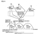
- Fig. 11 schematically shows a CDMA communication system.
- base stations 11, 12 and 13 cover predetermined areas respectively, each area being referred to as a cell.
- mobile machine 1 enters any one of the cells of the plurality of base stations 11, 12 and 13, it receives electric waves transmitted from a corresponding base station and sends electric waves to the base station.
- There are reflecting or obstructing objects such as buildings between mobile machine 1 and base stations 11, 12 and 13, so that not only straight electric waves but also reflected or diffracted waves are present between mobile machine 1 and base stations 11, 12 and 13.
- a receiving portion of mobile machine 1 receives synthesized electric waves that have passed through the multipath.
- the concept of handover is used in that a base station for communication is switched from one to another in accordance with a reception level of a base station in a mobile machine. That is, in a portable telephone, the cell of one base station cannot cover all communication areas, and a station for communication is switched from, for example, base station 11 to base stations 12 and 13 as mobile machine 1 moves.
- the reception level of each cell received by mobile machine 1 varies, providing an area that can receive only a signal from base station 11, an area that can receive only a signal from base station 12 and an area that can receive signals from both base stations 11 and 12 in accordance with movement of mobile machine 1.
- An area with the cells of both base stations 11 and 12 overlapped with each other is referred to as a handover area.
- a technique called soft handover in which electric waves are received from a plurality of base stations and synthesized, is used to perform control so as to prevent instantaneous interruption.
- the control is performed by a path search circuit and a finger/combiner circuit.
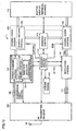
- Fig. 12 is a block diagram showing the entire configuration of the mobile machine operated by the CDMA system.
- a RF transmitter/receiver 102 converts a high-frequency signal received at an antenna 101 into a signal with a baseband bandwidth by filtering or down-converting, and pulls up a baseband signal output from a modulation portion 110 to a high-frequency signal by up-converting to transmit the signal from antenna 101.
- a baseband reception signal output from RF transmitter/receiver 102 is converted into a digital signal by an A/D converter 103 and is applied to a demodulation portion 104.
- Demodulation portion 104 includes a finger/combiner portion 105 and a search portion 106, detecting a desired signal timing from the reception signal and obtaining symbol data by inverse diffusion and in-phase synthesis (RAKE synthesis) to output the data to a channel codec portion 107.
- Search portion 106 includes a RAKE path detector 120 which will be described later.
- Channel codec portion 107 includes a channel decoder portion 108 and a channel coder portion 109 that perform error correction and error detection from the received symbol to estimate original data.
- Channel coder portion 109 performs redundant encoding on transmission information in order to enhance error resistance and outputs a transmission symbol to modulation portion 110.
- Modulation portion 110 performs primary modulation (data modulation) and secondary modulation (diffusion modulation) on the transmission symbol, and provides filtering to prevent interference among codes.
- a transmission baseband signal modulated at modulation portion 110 is converted into an analog signal by a D/A converter 111 and applied to RF transmitter/receiver 102.
- a timing signal generation circuit 112 generates various timing signals.
- a baseband control portion 113 performs timing control on demodulation portion 104, modulation portion 110 and channel codec portion 107 in accordance with a timing signal from timing signal generation circuit 112.
- Sequence control portion 114 performs control on communication with a base station.
- Adapter 115 establishes connection to a user interface such as voice communication or key operation and to peripheral devices (such as a personal computer).
- Fig. 13 is a block diagram showing an example of the RAKE path detector shown in Fig. 12, which is described in Japanese Patent Laying-Open No. 11-225093.
- a plurality of RAKE path detectors 120 are provided in order to observe delay profiles from digitized reception signals and to detect effective paths simultaneously for a plurality of channels or base stations.
- RAKE path detector 120 observes electric waves from a plurality of base stations 11, 12 and 13 shown in Fig. 1 and observes an effective path to utilize it in soft handover.
- Each of RAKE path detectors 120 includes a matched filter 121, a delay profile generation circuit 122, a memory 123 and an effective path detection circuit 124.
- h( ⁇ ) ⁇ s*(Ts - ⁇ ) (wherein ⁇ is an arbitrary constant and * is a complex conjugate) is obtained if noise n(t) is white.
- the filter having such an impulse response is called a matched filter for signal s(t). Use of such a matched filter allows accurate incoming time of electric waves to be obtained.
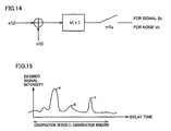
- Fig. 15 illustrates a delay profile.
- Fig. 11 when there are a plurality of propagation paths (multiple paths) between base stations 11, 12 and 13 and mobile machine 1, propagation time is different for each of the propagation paths. Signals that have passed through such multiple paths are observed by the matched filter to find a plurality of peaks during an observation period in accordance with delay time.
- the characteristic showing the intensity of a desired signal with respect to delay time as shown in Fig. 15 is called the delay profile.
- the delay profile is affected usually by fading and shadowing and varies dynamically.
- the first strong peak "a” in Fig. 15 shows a timing at which a strong electric wave arrives, the next weak peak "b” showing arrival of a weak electric wave with a delay, the next peak "c” showing arrival of an electric wave with a further delay.
- Matched filter 121 in RAKE path detector 120 observes the intensity of an electric wave with respect to delay dime shown in Fig. 15.
- Delay profile generation circuit 122 converts an output of matched filter 121 into a delay profile to be stored into memory 123.
- Effective path detection circuit 124 detects an effective path from the delay profile stored in the memory.
- a path allocation control circuit 125 allocates timing for the path detected by effective path detection circuit 124 to finger/combiner portion 105 as the timing of arrival of an electric wave.
- other RAKE detectors observe delay profiles of the other base stations to detect effective paths.
- RAKE path detector 120 must be provided in correspondence to each base station. That is, observation of the delay profiles of N base stations would require N matched filters.
- the matched filter has a large circuit scale and hence has a limited number of base stations to be observed. Increase of the base stations to be observed would disadvantageously increase the circuit scale, complexity in configuration and the number of components.
- a main object of the present invention is, therefore, to provide a radio mobile machine capable of having an increased number of base stations that can be observed at once without increase in a circuit scale.
- a reception portion receives a high-frequency signal from a base station and outputs a baseband signal.
- a profile measurement portion measures a delay profile of the signal from the base station based on the baseband signal.
- a control portion controls the delay profile measurement portion such that delay profiles for respective signals from a plurality of base stations by time division.
- a path detection portion detects an effective path to the base station based on the measured delay profiles.
- the delay profiles for the signals from the plurality of base stations are measured by time division, to measure the delay profiles of the plurality of base stations at once without increase in the circuit scale.
- control portion can vary the number of time divisions and respective operating time periods.
- the profile measurement portion includes a matched filter observing an intensity of a signal with respect to delay time based on the baseband signal, and a delay profile generation circuit generating a delay profiles based on the intensity of the signal with respect to the delay time observed by the matched filter.
- M profile measurement portions are provided, and delay profiles of N (M ⁇ N) base stations are observed.
- an averaging circuit averaging delay profiles by adding the measured delay profiles multiplied by a prescribed number smaller than 1 to a newly measured delay profile is further provided.
- a memory storing the measured delay profiles is further provided. Contents of the memory are cleared, with a prescribed number of the averaging circuit set as 0.
- control portion changes a measurement period and/or measurement timing at which a delay profile is measured based on a measured delay spread.
- Fig. 1 is a block diagram of a RAKE path detector according to one embodiment of the present invention.
- RAKE path detector 130 has a simplified configuration by providing a plurality of memories in RAKE path detector 120 shown in Fig. 13 and by controlling profile measurement circuit 138 by time division.
- RAKE path detector 130 includes a profile measurement circuit 138 constituted by a matched filter 131, a delay profile generation circuit 132 and a code generator 137, a demultiplexer 133, memories 141, 142, ..., 14N, a multiplexer 134, an effective path detection circuit 135, and a time division control circuit 136.
- Code generator 137 generates a code for searching each base station and applies the code to matched filter 131.
- Time division control circuit 136 switches back and forth between demultiplexer 133 and multiplexer 134 every time a profile of each base station is measured.
- Fig. 2 illustrates a method of storing a delay profile into a memory
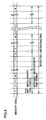
- Figs. 3A-3E are timing charts for illustrating operation in one embodiment of the present invention.
- code generator 137 When a profile is measured only for base station 11, code generator 137 generates a code corresponding to the base station, matched filter 131 measuring only the profile of that base station as shown in Fig. 3A, time division control circuit 136 controlling demultiplexer 133 such that the delay profile generated at delay profile generation circuit 132 is stored into memory 141 and controlling multiplexer 134 such that the stored delay profile is provided to effective path detection circuit 135.
- code generator 137 alternately generates respective codes for base stations 11 and 12.
- Matched filter 131 and delay profile generation circuit 132 alternately measure the delay profiles obtained based on the electric waves from base stations 11 and 12, as shown in Fig. 3B.
- Time division control circuit 136 controls demultiplexer 133 and multiplexer 134 by time division such that the delay profiles from base stations 11 and 12 are stored into memories 141 and 142 respectively and provided to effective path detector 135.
- code generator 137 alternately generates respective codes for base stations 11, 12, ... 1N.
- Matched filter 131 and delay profile generation circuit 132 alternately measure by time division the delay profiles obtained based on the electric waves from base stations 11, 12, ... 1N as shown in Fig. 3C.
- Time division control circuit 136 controls demultiplexer 133 and multiplexer 134 by time division such that the delay profiles from base stations 11, 12, ... 1N are stored into memories 141, 142, ... 14N, respectively, and provided to effective path detector 135, as shown in Fig. 2.
- Fig. 4 is a flowchart illustrating operation for reducing power consumption.
- the embodiment shown in Fig. 4 evaluates a fading pitch and path stability, to increase a pause period if the evaluated value is higher than a stable threshold and to reduce the pause period if the evaluated value is lower than an unstable threshold.
- the fading pitch is short, it is assumed that mobile machine 1 is moving fast, meaning that propagation environment tends to vary. Accordingly, the pause period is reduced whereas the measurement time is increased.
- the fading pitch is very long, it is assumed that mobile machine 1 has a very low moving speed or is almost stationary.
- the pause period is increased to optimize the operation rate, reducing power consumption.
- time division control circuit 136 causes code generator 137 to generate a code for base station 11 and to apply the code to matched filter 131.
- Demultiplexer 133 and multiplexer 134 is controlled by time division control circuit 136 by time division to operate memory 141 for the period of the unit measurement time for storing delay profiles and to provide the profiles to effective path detection circuit 135.
- the pause period comes. When a unit measurement time comes after the pause period, measurements of delay profiles are performed again. This can shorten actual measurement time compared to apparent measurement time, eliminating the need for operation of RAKE path detector 130 for that period of time, reducing power consumption.
- the delay profile of base station 11 is measured for one unit measurement time period, and thereafter the delay profile of base station 12 is measured for one unit measurement time period, as shown in Fig. 3E. This is followed by a pause period, and after the pause period, the delay profile of base station 11 is measured again for one unit measurement time period.
- a multiple number is made variable in time-division operation of profile measurement circuit 138 with respect to the number of cells for which delay profiles should be measured. If the number of cells to be measured is low or if delay profiles are stable, an operation stop period may be provided to lower the operation rate, reducing power consumption.
- Fig. 5 is a block diagram showing another embodiment of the present invention.
- a plurality of delay profiles are measured by one matched filter 131.
- measurement time per cell decreases as the number of cells increases, possibly deteriorating performance.
- Delay profiles for six cells are to be measured according to the specification, so that the performance is lowered to one-sixth in time division control.
- N cells e.g. six cells
- M ( ⁇ N) e.g. two
- N (six) storage memories for storing the delay profiles are used.
- M (two) each of matched filters 151, ..., 15M, code generators 161, ..., 16M, delay profile generation circuits 171, ..., 17M and demultiplexers 181, ..., 18M are provided, while the other components such as memories 141, 142, ... 14N, multiplexer 134, effective path detector 135 and time division control circuit 136 are configured as those in Fig. 1.
- Figs. 6A to 6D are timing charts for illustrating the operation of the embodiment shown in Fig. 5.
- time division control circuit 136 sets only matched filter 151, code generator 161 and multiplexer 181 in an operating state, while the other matched filters and the like are set in a non-operating state (off), as shown in Fig. 6B.
- the delay profile of cell 1 is constantly measured as shown in Fig. 6A.
- matched filter 151 When the delay profiles of N cells (e.g. six cells) are measured, matched filter 151 performs time division control such that the delay profiles of cells 1, 2 and 3 are sequentially measured, whereas matched filter 15M performs time division control such that the delay profiles of cells 4, 5 and 6 are sequentially measured.
- two matched filters 151 and 15M measure the delay profiles of six cells by time division control, only requiring two each of matched filters and delay profile generation circuits, allowing simplified configuration and reduced power consumption, though the performance is degraded to one-third compared to the case where a matched filter is provided for each cell.
- Fig. 7 is a block diagram showing a further embodiment of the present invention.
- Fig. 8 is a timing chart for illustrating the operation.
- the present embodiment is to add an averaging circuit 161 between the output of delay profile generation circuit 132 and demultiplexer 133 to the configuration of the embodiment shown in Fig. 1.
- a delay profile is ever changing due to a propagation environment such as fading. This causes variations with time in the strength or timing of a path. Because control for actually determining timing of demodulation is performed after observation of delay profiles, delay occurs in response time. Thus, a selected path is merely a result observed before actual use, and there is no guarantee that the path is optimal when allocated to a finger. In order to reduce an effect thereby, averaging circuit 161 is provided in the present embodiment. Ideally, a delay profile for e.g. 80 milliseconds is preferably measured and averaged, which however increases the memory capacity to a large extent and complicates the configuration.
- a technique is employed in that a most-recently-measured delay profile multiplied by a forgetting factor smaller than "1" is added to a newly measured delay profile.
- Averaging circuit 161 includes an adder 162 and a coefficient multiplier 163.
- Coefficient multiplier 163 multiplies the memory content output from multiplexer 134 by a forgetting factor smaller than "1" and applies the result to adder 162 via switch circuit 164.
- Adder 162 adds the profiles obtained so far that are weighted by a forgetting factor to a new delay profile corresponding to the cell for the read delay profile, to apply the addition result to demultiplexer 133.
- averaging circuit 161 is provided while the delay profiles stored in memories 141, 142, ... 14N are fed back to coefficient multiplier 163 and multiplied by a forgetting factor to add the resulting delay profiles to a newly measured delay profile.
- the adverse effect due to the delay in response time caused by control for actually determining timing of demodulation after observation can be reduced.
- an S/N ratio can be improved by an averaged gain.
- memories 141, 142, ..., 14N When a base station for communication via soft handover is switched or when a cell to be monitored by a peripheral cell monitor is switched, memories 141, 142, ..., 14N must be cleared in order to switch a cell to be observed. For instance, as shown in Fig. 9, if a profile 1 is written in addresses 0-1A and a profile 2 is written in addresses 1A-2A in the storage memory, and a profile N is further to be written into addresses 1A-2A, it is required to clear data in original profile 2. In general, clearing of a memory requires a dedicated circuit for writing 0 into each memory area, which increases not only time required but also power consumption.
- a configuration is implemented in that the output of coefficient multiplier 163 shown in Fig. 7 is applied to one input of switch circuit 164, "0" is applied to the other input thereof, and the output of switch circuit 164 is applied to demultiplexer 133.
- memories 141, 142, ... 14N are cleared, an input of switch circuit 164 is switched to the other side, and "0" is set as a forgetting factor for the period of unit observation time shown in Fig. 8.
- This allows new delay profiles to be written while clearing values remaining in the memories. That is, an effect similar to that of memory clearing can be obtained, eliminating the time required for memory clearing, and hence there is no increase in both circuit scale and power consumption.
- Figs. 10A to 10C each shows an observation period of a delay profile.
- a delay profile is measured constantly by an observation period (observation window) having a maximum width as shown in Fig. 10A, the delay profile is measured in which no effective path appears, increasing power consumption and a memory region used.
- the effective path can efficiently be measured. For instance, a delay spread (time difference between a path with a minimum delay and a path with a maximum delay) is measured that indicates the range (extent) where an effective path appears for an observation window, and if it is sufficiently small, the observation window may be made smaller accordingly and if necessary, the timing of the observation window may be shifted.
- a delay spread time difference between a path with a minimum delay and a path with a maximum delay
- the size and timing of an observation window for observing a delay profile is made variable based on a delay spread.
- matched filter 131 is so configured that the unit width of the observation window determined by the hardware configuration of matched filter 131 is small.
- Profile measurement circuit 138 is then controlled by time division such that an observation window used for observation is designated to matched filter 131 per unit measurement time.
- an observation window for delay profile generation circuit 132 is set large if the delay spread is large as shown in Fig. 10A, wherein sequential control is performed such that delay time of 0 to 199 chips are measured in the first unit measurement time period, and one delay profile from 0 to 399 chips is observed in four unit measurement time periods. Further, the observation window is set small if the delay spread is small as shown in Figs. 10B and 10C, wherein control is performed such that delay time of 100 to 199 chips are measured in the first unit measurement time period whereas 200 to 299 chips are measured in the next unit measurement time, and one delay profile from 100 to 299 chips is measured in two unit measurement time periods.
- a matched filter operated by time division for storing delay profiles of a plurality of base stations into a plurality of memories allows observation of the delay profiles of the plurality of base stations at once without increase in the circuit scale. This can be applicable to a radio mobile machine for radio communication such as a portable telephone.
Landscapes
- Engineering & Computer Science (AREA)
- Computer Networks & Wireless Communication (AREA)
- Signal Processing (AREA)
- Microelectronics & Electronic Packaging (AREA)
- Multimedia (AREA)
- Computer Hardware Design (AREA)
- Mobile Radio Communication Systems (AREA)
Abstract
A matched filter (131) extracts incoming time of signals from a
plurality of base stations by time division, based on a baseband signal
output from a RF transmitter/receiver (102). A delay profile generation
circuit (132) generates respective delay profiles based on the incoming time,
and the generated delay profiles are stored into memories (141, ..., 14N)
designated by a demultiplexer (133). An effective path detection circuit
(135) detects an effective path based on the stored delay profiles.
Description
The present invention relates to a radio mobile machine, and more
particularly, to a path search circuit in a portable telephone operated by a
code division multiple access system (hereinafter referred to as CDMA
communication system).
Fig. 11 schematically shows a CDMA communication system. In Fig.
11, base stations 11, 12 and 13 cover predetermined areas respectively,
each area being referred to as a cell. When mobile machine 1 enters any
one of the cells of the plurality of base stations 11, 12 and 13, it receives
electric waves transmitted from a corresponding base station and sends
electric waves to the base station. There are reflecting or obstructing
objects such as buildings between mobile machine 1 and base stations 11,
12 and 13, so that not only straight electric waves but also reflected or
diffracted waves are present between mobile machine 1 and base stations
11, 12 and 13. This produces a plurality of electric wave propagation paths
(multipath). A receiving portion of mobile machine 1 receives synthesized
electric waves that have passed through the multipath.
In mobile communication, the concept of handover is used in that a
base station for communication is switched from one to another in
accordance with a reception level of a base station in a mobile machine.
That is, in a portable telephone, the cell of one base station cannot cover all
communication areas, and a station for communication is switched from, for
example, base station 11 to base stations 12 and 13 as mobile machine 1
moves. Here, as shown in Fig. 11, the reception level of each cell received
by mobile machine 1 varies, providing an area that can receive only a signal
from base station 11, an area that can receive only a signal from base
station 12 and an area that can receive signals from both base stations 11
and 12 in accordance with movement of mobile machine 1. An area with
the cells of both base stations 11 and 12 overlapped with each other is
referred to as a handover area.
In the CDMA system, a technique called soft handover, in which
electric waves are received from a plurality of base stations and synthesized,
is used to perform control so as to prevent instantaneous interruption.
The control is performed by a path search circuit and a finger/combiner
circuit.
Fig. 12 is a block diagram showing the entire configuration of the
mobile machine operated by the CDMA system. In Fig. 12, a RF
transmitter/receiver 102 converts a high-frequency signal received at an
antenna 101 into a signal with a baseband bandwidth by filtering or down-converting,
and pulls up a baseband signal output from a modulation
portion 110 to a high-frequency signal by up-converting to transmit the
signal from antenna 101.
A baseband reception signal output from RF transmitter/receiver 102
is converted into a digital signal by an A/D converter 103 and is applied to a
demodulation portion 104. Demodulation portion 104 includes a
finger/combiner portion 105 and a search portion 106, detecting a desired
signal timing from the reception signal and obtaining symbol data by
inverse diffusion and in-phase synthesis (RAKE synthesis) to output the
data to a channel codec portion 107. Search portion 106 includes a RAKE
path detector 120 which will be described later. Channel codec portion 107
includes a channel decoder portion 108 and a channel coder portion 109
that perform error correction and error detection from the received symbol
to estimate original data.
A timing signal generation circuit 112 generates various timing
signals. A baseband control portion 113 performs timing control on
demodulation portion 104, modulation portion 110 and channel codec
portion 107 in accordance with a timing signal from timing signal
generation circuit 112. Sequence control portion 114 performs control on
communication with a base station. Adapter 115 establishes connection to
a user interface such as voice communication or key operation and to
peripheral devices (such as a personal computer).
Fig. 13 is a block diagram showing an example of the RAKE path
detector shown in Fig. 12, which is described in Japanese Patent Laying-Open
No. 11-225093. A plurality of RAKE path detectors 120 are provided
in order to observe delay profiles from digitized reception signals and to
detect effective paths simultaneously for a plurality of channels or base
stations. RAKE path detector 120 observes electric waves from a plurality
of base stations 11, 12 and 13 shown in Fig. 1 and observes an effective
path to utilize it in soft handover. Each of RAKE path detectors 120
includes a matched filter 121, a delay profile generation circuit 122, a
memory 123 and an effective path detection circuit 124.
Matched filter 121 is designed such that an impulse response of h(τ)
is obtained if noise n(t) is applied to a signal s(t) as shown in Fig. 14, and
that a signal-to-noise ratio at the output of time Ts of the filter becomes
maximum if r(t) = s(t) + n(t) is input. Here, it is known that
h(τ) = λs*(Ts -τ)
(wherein λ is an arbitrary constant and * is a complex conjugate)
is obtained if noise n(t) is white. The filter having such an impulse response is called a matched filter for signal s(t). Use of such a matched filter allows accurate incoming time of electric waves to be obtained.
is obtained if noise n(t) is white. The filter having such an impulse response is called a matched filter for signal s(t). Use of such a matched filter allows accurate incoming time of electric waves to be obtained.
Fig. 15 illustrates a delay profile. As shown in Fig. 11, when there
are a plurality of propagation paths (multiple paths) between base stations
11, 12 and 13 and mobile machine 1, propagation time is different for each
of the propagation paths. Signals that have passed through such multiple
paths are observed by the matched filter to find a plurality of peaks during
an observation period in accordance with delay time.
The characteristic showing the intensity of a desired signal with
respect to delay time as shown in Fig. 15 is called the delay profile. In
mobile unit communication, the delay profile is affected usually by fading
and shadowing and varies dynamically. The first strong peak "a" in Fig.
15 shows a timing at which a strong electric wave arrives, the next weak
peak "b" showing arrival of a weak electric wave with a delay, the next peak
"c" showing arrival of an electric wave with a further delay.
Matched filter 121 in RAKE path detector 120 observes the intensity
of an electric wave with respect to delay dime shown in Fig. 15. Delay
profile generation circuit 122 converts an output of matched filter 121 into a
delay profile to be stored into memory 123. Effective path detection circuit
124 detects an effective path from the delay profile stored in the memory.
A path allocation control circuit 125 allocates timing for the path detected
by effective path detection circuit 124 to finger/combiner portion 105 as the
timing of arrival of an electric wave. Likewise, other RAKE detectors
observe delay profiles of the other base stations to detect effective paths.
Thus, RAKE path detector 120 must be provided in correspondence
to each base station. That is, observation of the delay profiles of N base
stations would require N matched filters. However, the matched filter has
a large circuit scale and hence has a limited number of base stations to be
observed. Increase of the base stations to be observed would
disadvantageously increase the circuit scale, complexity in configuration
and the number of components.
A main object of the present invention is, therefore, to provide a radio
mobile machine capable of having an increased number of base stations
that can be observed at once without increase in a circuit scale.
In the present invention, a reception portion receives a high-frequency
signal from a base station and outputs a baseband signal. A
profile measurement portion measures a delay profile of the signal from the
base station based on the baseband signal. A control portion controls the
delay profile measurement portion such that delay profiles for respective
signals from a plurality of base stations by time division. A path detection
portion detects an effective path to the base station based on the measured
delay profiles.
Thus, according to the present invention, the delay profiles for the
signals from the plurality of base stations are measured by time division, to
measure the delay profiles of the plurality of base stations at once without
increase in the circuit scale.
More preferably, the control portion can vary the number of time
divisions and respective operating time periods.
Moreover, the profile measurement portion includes a matched filter
observing an intensity of a signal with respect to delay time based on the
baseband signal, and a delay profile generation circuit generating a delay
profiles based on the intensity of the signal with respect to the delay time
observed by the matched filter.
Furthermore, M profile measurement portions are provided, and
delay profiles of N (M<N) base stations are observed.
In addition, an averaging circuit averaging delay profiles by adding
the measured delay profiles multiplied by a prescribed number smaller
than 1 to a newly measured delay profile is further provided.
A memory storing the measured delay profiles is further provided.
Contents of the memory are cleared, with a prescribed number of the
averaging circuit set as 0.
Moreover, the control portion changes a measurement period and/or
measurement timing at which a delay profile is measured based on a
measured delay spread.
Fig. 1 is a block diagram of a RAKE path detector according to one
embodiment of the present invention. In Fig. 1, RAKE path detector 130
has a simplified configuration by providing a plurality of memories in
RAKE path detector 120 shown in Fig. 13 and by controlling profile
measurement circuit 138 by time division.
Thus, RAKE path detector 130 includes a profile measurement
circuit 138 constituted by a matched filter 131, a delay profile generation
circuit 132 and a code generator 137, a demultiplexer 133, memories 141,
142, ..., 14N, a multiplexer 134, an effective path detection circuit 135, and
a time division control circuit 136.
Fig. 2 illustrates a method of storing a delay profile into a memory,
while Figs. 3A-3E are timing charts for illustrating operation in one
embodiment of the present invention.
When a profile is measured only for base station 11, code generator
137 generates a code corresponding to the base station, matched filter 131
measuring only the profile of that base station as shown in Fig. 3A, time
division control circuit 136 controlling demultiplexer 133 such that the
delay profile generated at delay profile generation circuit 132 is stored into
memory 141 and controlling multiplexer 134 such that the stored delay
profile is provided to effective path detection circuit 135.
When the profiles of base stations 11 and 12 are measured, code
generator 137 alternately generates respective codes for base stations 11
and 12. Matched filter 131 and delay profile generation circuit 132
alternately measure the delay profiles obtained based on the electric waves
from base stations 11 and 12, as shown in Fig. 3B. Time division control
circuit 136 controls demultiplexer 133 and multiplexer 134 by time division
such that the delay profiles from base stations 11 and 12 are stored into
memories 141 and 142 respectively and provided to effective path detector
135.
When the profiles of base stations 11, 12, ... 1N are measured, code
generator 137 alternately generates respective codes for base stations 11,
12, ... 1N. Matched filter 131 and delay profile generation circuit 132
alternately measure by time division the delay profiles obtained based on
the electric waves from base stations 11, 12, ... 1N as shown in Fig. 3C.
Time division control circuit 136 controls demultiplexer 133 and
multiplexer 134 by time division such that the delay profiles from base
stations 11, 12, ... 1N are stored into memories 141, 142, ... 14N,
respectively, and provided to effective path detector 135, as shown in Fig. 2.
Fig. 4 is a flowchart illustrating operation for reducing power
consumption. The embodiment shown in Fig. 4 evaluates a fading pitch
and path stability, to increase a pause period if the evaluated value is
higher than a stable threshold and to reduce the pause period if the
evaluated value is lower than an unstable threshold. Thus, if the fading
pitch is short, it is assumed that mobile machine 1 is moving fast, meaning
that propagation environment tends to vary. Accordingly, the pause
period is reduced whereas the measurement time is increased. On the
contrary, if the fading pitch is very long, it is assumed that mobile machine
1 has a very low moving speed or is almost stationary. Here, the pause
period is increased to optimize the operation rate, reducing power
consumption.
More specifically, if the received electric wave is rather strong or if
there is no change in the propagation environment, constant measurement
of profiles is not required, and hence the delay profiles are measured for the
period of a predetermined unit process time as shown in Fig. 3D. That is,
in order to measure only the delay profile of base station 11 for the unit
measurement time as shown in Fig. 3D, time division control circuit 136
causes code generator 137 to generate a code for base station 11 and to
apply the code to matched filter 131. Demultiplexer 133 and multiplexer
134 is controlled by time division control circuit 136 by time division to
operate memory 141 for the period of the unit measurement time for storing
delay profiles and to provide the profiles to effective path detection circuit
135. After the unit measurement time has elapsed, the pause period
comes. When a unit measurement time comes after the pause period,
measurements of delay profiles are performed again. This can shorten
actual measurement time compared to apparent measurement time,
eliminating the need for operation of RAKE path detector 130 for that
period of time, reducing power consumption.
Likewise, when the delay profiles for two base stations 11, 12 are
emasured with low power consumption, the delay profile of base station 11
is measured for one unit measurement time period, and thereafter the delay
profile of base station 12 is measured for one unit measurement time period,
as shown in Fig. 3E. This is followed by a pause period, and after the
pause period, the delay profile of base station 11 is measured again for one
unit measurement time period.
Therefore, according to the present embodiment, a multiple number
is made variable in time-division operation of profile measurement circuit
138 with respect to the number of cells for which delay profiles should be
measured. If the number of cells to be measured is low or if delay profiles
are stable, an operation stop period may be provided to lower the operation
rate, reducing power consumption.
Fig. 5 is a block diagram showing another embodiment of the present
invention. In the embodiment shown in Fig. 1, a plurality of delay profiles
are measured by one matched filter 131. However, measurement time per
cell decreases as the number of cells increases, possibly deteriorating
performance. Delay profiles for six cells are to be measured according to
the specification, so that the performance is lowered to one-sixth in time
division control. Thus, in the embodiment shown in Fig. 5, in order to
measure delay profiles for N cells (e.g. six cells), M (<N) (e.g. two) matched
filters and N (six) storage memories for storing the delay profiles are used.
More specifically, M (two) each of matched filters 151, ..., 15M, code
generators 161, ..., 16M, delay profile generation circuits 171, ..., 17M and
demultiplexers 181, ..., 18M are provided, while the other components such
as memories 141, 142, ... 14N, multiplexer 134, effective path detector 135
and time division control circuit 136 are configured as those in Fig. 1.
Figs. 6A to 6D are timing charts for illustrating the operation of the
embodiment shown in Fig. 5. In Figs. 6A to 6D, when only cell 1 is
received, time division control circuit 136 sets only matched filter 151, code
generator 161 and multiplexer 181 in an operating state, while the other
matched filters and the like are set in a non-operating state (off), as shown
in Fig. 6B. As a result, the delay profile of cell 1 is constantly measured as
shown in Fig. 6A.
When the delay profiles of N cells (e.g. six cells) are measured,
matched filter 151 performs time division control such that the delay
profiles of cells 1, 2 and 3 are sequentially measured, whereas matched
filter 15M performs time division control such that the delay profiles of cells
4, 5 and 6 are sequentially measured.
Hence, according to the present embodiment, two matched filters 151
and 15M, for example, measure the delay profiles of six cells by time
division control, only requiring two each of matched filters and delay profile
generation circuits, allowing simplified configuration and reduced power
consumption, though the performance is degraded to one-third compared to
the case where a matched filter is provided for each cell.
Fig. 7 is a block diagram showing a further embodiment of the
present invention. Fig. 8 is a timing chart for illustrating the operation.
The present embodiment is to add an averaging circuit 161 between the
output of delay profile generation circuit 132 and demultiplexer 133 to the
configuration of the embodiment shown in Fig. 1.
In general, a delay profile is ever changing due to a propagation
environment such as fading. This causes variations with time in the
strength or timing of a path. Because control for actually determining
timing of demodulation is performed after observation of delay profiles,
delay occurs in response time. Thus, a selected path is merely a result
observed before actual use, and there is no guarantee that the path is
optimal when allocated to a finger. In order to reduce an effect thereby,
averaging circuit 161 is provided in the present embodiment. Ideally, a
delay profile for e.g. 80 milliseconds is preferably measured and averaged,
which however increases the memory capacity to a large extent and
complicates the configuration.
In the present embodiment, therefore, a technique is employed in
that a most-recently-measured delay profile multiplied by a forgetting
factor smaller than "1" is added to a newly measured delay profile.
Thus, the delay profiles stored in memories 141, 142, ..., 14N are
read by multiplexer 134 by time division and provided to averaging circuit
161. Averaging circuit 161 includes an adder 162 and a coefficient
multiplier 163. Coefficient multiplier 163 multiplies the memory content
output from multiplexer 134 by a forgetting factor smaller than "1" and
applies the result to adder 162 via switch circuit 164. Adder 162 adds the
profiles obtained so far that are weighted by a forgetting factor to a new
delay profile corresponding to the cell for the read delay profile, to apply the
addition result to demultiplexer 133.
As such, averaging circuit 161 is provided while the delay profiles
stored in memories 141, 142, ... 14N are fed back to coefficient multiplier
163 and multiplied by a forgetting factor to add the resulting delay profiles
to a newly measured delay profile. Thus, the adverse effect due to the
delay in response time caused by control for actually determining timing of
demodulation after observation can be reduced. Moreover, an S/N ratio
can be improved by an averaged gain.
When a base station for communication via soft handover is switched
or when a cell to be monitored by a peripheral cell monitor is switched,
memories 141, 142, ..., 14N must be cleared in order to switch a cell to be
observed. For instance, as shown in Fig. 9, if a profile 1 is written in
addresses 0-1A and a profile 2 is written in addresses 1A-2A in the storage
memory, and a profile N is further to be written into addresses 1A-2A, it is
required to clear data in original profile 2. In general, clearing of a
memory requires a dedicated circuit for writing 0 into each memory area,
which increases not only time required but also power consumption.
Thus, a configuration is implemented in that the output of coefficient
multiplier 163 shown in Fig. 7 is applied to one input of switch circuit 164,
"0" is applied to the other input thereof, and the output of switch circuit 164
is applied to demultiplexer 133. When memories 141, 142, ... 14N are
cleared, an input of switch circuit 164 is switched to the other side, and "0"
is set as a forgetting factor for the period of unit observation time shown in
Fig. 8. This allows new delay profiles to be written while clearing values
remaining in the memories. That is, an effect similar to that of memory
clearing can be obtained, eliminating the time required for memory clearing,
and hence there is no increase in both circuit scale and power consumption.
Figs. 10A to 10C each shows an observation period of a delay profile.
If a delay profile is measured constantly by an observation period
(observation window) having a maximum width as shown in Fig. 10A, the
delay profile is measured in which no effective path appears, increasing
power consumption and a memory region used.
Here, if the delay profile is observed only in a range where an
effective path appears, the effective path can efficiently be measured. For
instance, a delay spread (time difference between a path with a minimum
delay and a path with a maximum delay) is measured that indicates the
range (extent) where an effective path appears for an observation window,
and if it is sufficiently small, the observation window may be made smaller
accordingly and if necessary, the timing of the observation window may be
shifted.
In the present embodiment, therefore, the size and timing of an
observation window for observing a delay profile is made variable based on
a delay spread. Thus, matched filter 131 is so configured that the unit
width of the observation window determined by the hardware configuration
of matched filter 131 is small. Profile measurement circuit 138 is then
controlled by time division such that an observation window used for
observation is designated to matched filter 131 per unit measurement time.
For instance, when matched filter 131 is configured to have a unit
width of 100 chips, an observation window for delay profile generation
circuit 132 is set large if the delay spread is large as shown in Fig. 10A,
wherein sequential control is performed such that delay time of 0 to 199
chips are measured in the first unit measurement time period, and one
delay profile from 0 to 399 chips is observed in four unit measurement time
periods. Further, the observation window is set small if the delay spread
is small as shown in Figs. 10B and 10C, wherein control is performed such
that delay time of 100 to 199 chips are measured in the first unit
measurement time period whereas 200 to 299 chips are measured in the
next unit measurement time, and one delay profile from 100 to 299 chips is
measured in two unit measurement time periods.
Moreover, when a plurality of cells are used for soft handover, similar
control is performed to set small an observation window that is to be
allocated to each cell, reducing the memory capacity storing a delay profile
per cell. Here, signals of the same content are received from a plurality of
base stations, allowing sufficient reception gain even though the
observation window is made small, preventing increase in total size of the
memory. On the contrary, when a signal of one cell is received, the
observation window is set large, allowing control such that the reception
gain is ensured.
According to the present invention, a matched filter operated by time
division for storing delay profiles of a plurality of base stations into a
plurality of memories allows observation of the delay profiles of the
plurality of base stations at once without increase in the circuit scale. This
can be applicable to a radio mobile machine for radio communication such
as a portable telephone.
Claims (14)
- A radio mobile machine, comprising:a receiving portion (102) receiving a high-frequency signal from a base station to output a baseband signal;a profile measurement portion (138) measuring a delay profile of a signal from said base station based on the baseband signal output from said receiving portion;a control portion (136) controlling said delay profile measurement portion such that a plurality of delay profiles for signals from respective base stations are measured by time division; anda path detection portion (135) detecting an effective path to said base station based on said measured delay profiles.
- The radio mobile machine according to claim 1, wherein said control portion can vary the number of time divisions and respective operating time periods.
- The radio mobile machine according to claim 1, wherein
said profile measurement portion includes
a matched filter (131, 151, ..., 15M) observing an intensity of a signal with respect to delay time based on said baseband signal, and
a delay profile generation circuit (132, 171, ... 17M) generating said delay profile based on the intensity of the signal with respect to the delay time observed by said matched filter. - The radio mobile machine according to claim 1, wherein
M said profile measurement portions are provided, and
delay profiles of N (M<N) base stations are observed. - The radio mobile machine according to claim 1, further comprising an averaging circuit (161) averaging delay profiles by adding the measured delay profile multiplied by a prescribed number smaller than 1 to a newly measured delay profile.
- The radio mobile machine according to claim 5, further comprising a memory (141, ..., 14N) storing the measured delay profile,
contents of said memory being cleared, with a prescribed number of said averaging circuit set as 0. - The radio mobile machine according to claim 1, wherein said control portion changes a measurement period and/or measurement timing at which a delay profile is measured based on a measured delay spread.
- A radio mobile machine, comprising:a receiving portion (102) receiving a high-frequency signal from a base station to output a baseband signal;a profile measurement portion (138) measuring a delay profile of a signal from said base station based on the baseband signal output from said reception portion;a control portion (136) controlling said delay profile measurement portion such that a delay profile of a signal from one base station is intermittently measured by time division; anda path detection portion (135) detecting an effective path to said base station based on said measured delay profile.
- The radio mobile machine according to claim 8, wherein said control portion can vary the number of time divisions and respective operating time periods.
- The radio mobile machine according to claim 8, wherein
said profile measurement portion includes
a matched filter (131, 151, ..., 15M) observing an intensity of a signal with respect to delay time based on said baseband signal, and
a delay profile generation circuit (132, 171, ..., 17M) generating said delay profile, based on the intensity of the signal with respect to the delay time observed by said matched filter. - The radio mobile machine according to claim 8, wherein
M said profile measurement portions are provided, and
delay profiles of (M<N) base stations are observed. - The radio mobile machine according to claim 8, further comprising an averaging circuit (161) averaging delay profiles by adding the measured delay profile multiplied by a prescribed number smaller than 1 to a newly measured delay profile.
- The radio mobile machine according to claim 12, further comprising a memory (141, ..., 14N) storing the measured delay profile,
contents of said memory being cleared, with a prescribed number of said averaging circuit set as 0. - The radio mobile machine according to claim 8, wherein said control portion changes a measurement period and/or measurement timing at which a delay profile is measured based on a measured delay spread.
Applications Claiming Priority (1)
| Application Number | Priority Date | Filing Date | Title |
|---|---|---|---|
| PCT/JP2001/007661 WO2003024009A1 (en) | 2001-09-04 | 2001-09-04 | Radio mobile device |
Publications (2)
| Publication Number | Publication Date |
|---|---|
| EP1424797A1 true EP1424797A1 (en) | 2004-06-02 |
| EP1424797A4 EP1424797A4 (en) | 2006-08-02 |
Family
ID=11737701
Family Applications (1)
| Application Number | Title | Priority Date | Filing Date |
|---|---|---|---|
| EP01961361A Withdrawn EP1424797A4 (en) | 2001-09-04 | 2001-09-04 | MOBILE DEVICE |
Country Status (5)
| Country | Link |
|---|---|
| US (1) | US20040029547A1 (en) |
| EP (1) | EP1424797A4 (en) |
| JP (1) | JP3989900B2 (en) |
| CN (1) | CN1533645A (en) |
| WO (1) | WO2003024009A1 (en) |
Families Citing this family (6)
| Publication number | Priority date | Publication date | Assignee | Title |
|---|---|---|---|---|
| US20040042411A1 (en) * | 2002-08-30 | 2004-03-04 | Erik Dahlback | Method and apparatus for controlling the rate of path searching in a communications system |
| JP4540434B2 (en) * | 2004-09-08 | 2010-09-08 | パナソニック株式会社 | Path search processing apparatus and processing method |
| JP2006101308A (en) * | 2004-09-30 | 2006-04-13 | Fujitsu Ltd | Radio base station apparatus and path search method |
| US7848388B2 (en) * | 2006-08-08 | 2010-12-07 | Sony Ericsson Mobile Communications Ab | Minimizing estimation time for rake fingers with help of a speed sensor |
| JP4836829B2 (en) * | 2007-02-26 | 2011-12-14 | 富士通株式会社 | Receiving device, path detecting device, method and computer program used in CDMA base station |
| US9276629B2 (en) * | 2011-11-17 | 2016-03-01 | Intel Deutschland Gmbh | Rake receiver circuit and method for operating a rake receiver circuit |
Family Cites Families (6)
| Publication number | Priority date | Publication date | Assignee | Title |
|---|---|---|---|---|
| ES2301896T3 (en) * | 1997-07-17 | 2008-07-01 | Matsushita Electric Industrial Co., Ltd | SYNCHRONIZATION PROCEDURE FOR A CDMA SYSTEM. |
| JP3891373B2 (en) * | 1998-03-26 | 2007-03-14 | ソニー株式会社 | Demodulator and demodulation method |
| JP3741881B2 (en) * | 1998-11-16 | 2006-02-01 | 富士通株式会社 | Receiver used in CDMA communication |
| JP2000278176A (en) * | 1999-03-19 | 2000-10-06 | Sanyo Electric Co Ltd | Delay profile measurement device |
| JP2000286768A (en) * | 1999-03-29 | 2000-10-13 | Kokusai Electric Co Ltd | CDMA mobile station device |
| FI19992734A7 (en) * | 1999-12-20 | 2001-06-21 | Nokia Corp | Method for receiving a spread spectrum signal and receiver |
-
2001
- 2001-09-04 JP JP2003527932A patent/JP3989900B2/en not_active Expired - Fee Related
- 2001-09-04 WO PCT/JP2001/007661 patent/WO2003024009A1/en not_active Ceased
- 2001-09-04 CN CNA018151175A patent/CN1533645A/en active Pending
- 2001-09-04 EP EP01961361A patent/EP1424797A4/en not_active Withdrawn
- 2001-09-04 US US10/363,263 patent/US20040029547A1/en not_active Abandoned
Also Published As
| Publication number | Publication date |
|---|---|
| JP3989900B2 (en) | 2007-10-10 |
| US20040029547A1 (en) | 2004-02-12 |
| EP1424797A4 (en) | 2006-08-02 |
| CN1533645A (en) | 2004-09-29 |
| WO2003024009A1 (en) | 2003-03-20 |
| JPWO2003024009A1 (en) | 2004-12-24 |
Similar Documents
| Publication | Publication Date | Title |
|---|---|---|
| EP1096711B1 (en) | CDMA receiving method and circuit | |
| US5936999A (en) | Receiver and method for generating spreading codes in a receiver | |
| JP2937994B1 (en) | Cellular system, mobile portable device, base station device, and optimal path detection method and device | |
| JP3447897B2 (en) | CDMA wireless communication device | |
| EP0615355B1 (en) | Mobile station and cell selecting method for code division multiplex access mobile communication | |
| EP1069708B1 (en) | Circuit for simultaneously performing path search and antenna directivity control | |
| JPH1051355A (en) | Spread spectrum communication equipment | |
| EP0808031B1 (en) | Spread spectrum multi-path demodulator | |
| JP3369513B2 (en) | Communication terminal device and wireless reception method | |
| US7042862B1 (en) | Path searching method and device | |
| EP1906544A2 (en) | Code synchronization method and receiver | |
| EP1164710B1 (en) | Spread spectrum receiver and spread spectrum receiving method | |
| EP1424797A1 (en) | Radio mobile device | |
| US7062284B2 (en) | Receiver and reception method | |
| EP1628409B1 (en) | A power level measuring device and a mobile station | |
| JP2000091973A (en) | RAKE synthesis circuit | |
| US6807223B2 (en) | Method of performing code synchronization, and receiver | |
| US9264098B2 (en) | Process for finger insertion and removal in a rake receiver and receiver for carrying out the process | |
| KR100486550B1 (en) | A device and a operating method of estimating doppler frequency in rake receiver | |
| JP2006140631A (en) | Frequency control device | |
| KR20030058915A (en) | Method and apparatus for compensating channel in mobile communication terminal | |
| JP2002204184A (en) | CDMA receiving apparatus and CDMA receiving method | |
| JP2007151029A (en) | Synchronous tracking circuit and cdma receiver |
Legal Events
| Date | Code | Title | Description |
|---|---|---|---|
| PUAI | Public reference made under article 153(3) epc to a published international application that has entered the european phase |
Free format text: ORIGINAL CODE: 0009012 |
|
| 17P | Request for examination filed |
Effective date: 20030310 |
|
| AK | Designated contracting states |
Kind code of ref document: A1 Designated state(s): AT BE CH CY DE DK ES FI FR GB GR IE IT LI LU MC NL PT SE TR |
|
| RAP1 | Party data changed (applicant data changed or rights of an application transferred) |
Owner name: MITSUBISHI DENKI KABUSHIKI KAISHA |
|
| STAA | Information on the status of an ep patent application or granted ep patent |
Free format text: STATUS: THE APPLICATION HAS BEEN WITHDRAWN |
|
| A4 | Supplementary search report drawn up and despatched |
Effective date: 20060630 |
|
| 18W | Application withdrawn |
Effective date: 20060628 |