EP1424766A1 - Régulateur de tension à découpage - Google Patents
Régulateur de tension à découpage Download PDFInfo
- Publication number
- EP1424766A1 EP1424766A1 EP02425737A EP02425737A EP1424766A1 EP 1424766 A1 EP1424766 A1 EP 1424766A1 EP 02425737 A EP02425737 A EP 02425737A EP 02425737 A EP02425737 A EP 02425737A EP 1424766 A1 EP1424766 A1 EP 1424766A1
- Authority
- EP
- European Patent Office
- Prior art keywords
- signal
- mos transistor
- current
- output terminal
- representative
- Prior art date
- Legal status (The legal status is an assumption and is not a legal conclusion. Google has not performed a legal analysis and makes no representation as to the accuracy of the status listed.)
- Withdrawn
Links
Images


Classifications
-
- H—ELECTRICITY
- H02—GENERATION; CONVERSION OR DISTRIBUTION OF ELECTRIC POWER
- H02M—APPARATUS FOR CONVERSION BETWEEN AC AND AC, BETWEEN AC AND DC, OR BETWEEN DC AND DC, AND FOR USE WITH MAINS OR SIMILAR POWER SUPPLY SYSTEMS; CONVERSION OF DC OR AC INPUT POWER INTO SURGE OUTPUT POWER; CONTROL OR REGULATION THEREOF
- H02M3/00—Conversion of dc power input into dc power output
- H02M3/02—Conversion of dc power input into dc power output without intermediate conversion into ac
- H02M3/04—Conversion of dc power input into dc power output without intermediate conversion into ac by static converters
- H02M3/10—Conversion of dc power input into dc power output without intermediate conversion into ac by static converters using discharge tubes with control electrode or semiconductor devices with control electrode
- H02M3/145—Conversion of dc power input into dc power output without intermediate conversion into ac by static converters using discharge tubes with control electrode or semiconductor devices with control electrode using devices of a triode or transistor type requiring continuous application of a control signal
- H02M3/155—Conversion of dc power input into dc power output without intermediate conversion into ac by static converters using discharge tubes with control electrode or semiconductor devices with control electrode using devices of a triode or transistor type requiring continuous application of a control signal using semiconductor devices only
- H02M3/156—Conversion of dc power input into dc power output without intermediate conversion into ac by static converters using discharge tubes with control electrode or semiconductor devices with control electrode using devices of a triode or transistor type requiring continuous application of a control signal using semiconductor devices only with automatic control of output voltage or current, e.g. switching regulators
-
- H—ELECTRICITY
- H02—GENERATION; CONVERSION OR DISTRIBUTION OF ELECTRIC POWER
- H02M—APPARATUS FOR CONVERSION BETWEEN AC AND AC, BETWEEN AC AND DC, OR BETWEEN DC AND DC, AND FOR USE WITH MAINS OR SIMILAR POWER SUPPLY SYSTEMS; CONVERSION OF DC OR AC INPUT POWER INTO SURGE OUTPUT POWER; CONTROL OR REGULATION THEREOF
- H02M1/00—Details of apparatus for conversion
- H02M1/0003—Details of control, feedback or regulation circuits
- H02M1/0009—Devices or circuits for detecting current in a converter
-
- H—ELECTRICITY
- H02—GENERATION; CONVERSION OR DISTRIBUTION OF ELECTRIC POWER
- H02M—APPARATUS FOR CONVERSION BETWEEN AC AND AC, BETWEEN AC AND DC, OR BETWEEN DC AND DC, AND FOR USE WITH MAINS OR SIMILAR POWER SUPPLY SYSTEMS; CONVERSION OF DC OR AC INPUT POWER INTO SURGE OUTPUT POWER; CONTROL OR REGULATION THEREOF
- H02M1/00—Details of apparatus for conversion
- H02M1/0003—Details of control, feedback or regulation circuits
- H02M1/0025—Arrangements for modifying reference values, feedback values or error values in the control loop of a converter
Definitions
- the present invention refers to a switching voltage regulator.
- Particularly such power suppliers must provide higher and higher currents and lower and lower voltages.
- Each regulator comprises at least one MOS power transistor; particularly some regulators comprise a pair of MOS transistors or several pairs of MOS transistors which are arranged in parallel to each others and which are connected with a single output terminal by means of an inductance for each transistor pair (Multi-phase converters).
- the output currents of said pairs of transistors are automatically balanced by means of a control operation which detects each single current by detecting the voltage drop between the drain and source terminals of the MOS transistor. This voltage drop is also employed for implementing a well precise and programmable load regulation as a function of the current provided to the load, as it is required from particular loads such as the microprocessors.
- the MOS transistors are provided internally of a resistance between the drain and source terminals in the conduction or firing phase, known as on or conduction resistance Rdson, which changes with the temperature and which, for this reason, can cause variations of the voltage signal between the drain and source terminals of the MOS transistor with currents of the same value.
- Rdson on or conduction resistance
- the thermal variation of the on resistance (Rdson) of the MOS may cause very high variations of the voltage regulated by the power suppliers which employ the voltage detected between the terminals of the MOS transistor for regulating the output voltage on the load to be supplied. This may bring to non-respect of some specifications of the loads such as the microprocessors.
- a possibility to avoid the variations of the voltage detected between the terminals of the MOS transistor of the voltage regulators consists of adding and consequently using measurement elements that are substantially invariant in temperature, for example resistors known as "sense resistors".
- the signal measured between the terminals of the sense resistors acts in the control operation of the MOS transistor for regulating suitably the output voltage of the regulator.
- resistors have thermal variations lower than the resistance Rdson, are very precise but the high precision thereof is compromised by the high contact resistance due to the welding thereof on the printed circuit of the regulator. Also the power dissipated by the sense resistors decreases the effectiveness of all the regulator and the use thereof causes a higher cost of all the appliance.
- this object is attained by means of a switching voltage regulator adapted for providing a regulated voltage at an output terminal, comprising at least one MOS transistor having a non-drivable terminal coupled with said output terminal and a control circuit receiving a signal that is representative of the current signal flowing in said MOS transistor, characterized in that said control circuit comprises a compensation device adapted for cancelling the thermal variation of said signal that is representative of the current signal flowing in said MOS transistor.
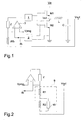
- a switching regulator according to prior art is shown; said regulator comprises two MOS power transistors M1 and M2 where the source terminal of the transistor M1 is in common with the drain terminal of the transistor M2 and it is connected with an inductance L the other terminal of which is the output terminal of the regulator.
- the drain terminal of the transistor M1 is connected with an input voltage Vin while the source terminal of the transistor M2 is connected to ground.
- the gate terminals of the transistors M1 and M2 (which may constitute even the electric equivalent of more MOS transistors connected with each others in parallel) are driven by means of a control circuitry 1.
- the transistors M1 and M2 may be discrete components or may be integrated in the same chip with the control circuitry 1.
- the current flowing between the drain and source terminals of the transistor M2 is detected by means of a detecting device 2 that preferably comprises an amplifier able to convert the voltage drop between the terminals of the transistor M2 into a proportional current signal Ifb.
- the detected current Ifb is in input at the inverting terminal of an error operational amplifier 3 having the non-inverting terminal connected with a reference voltage Vprog (for example of about 1.5 V) and the output terminal connected with an impedance Z the other terminal of which is connected with the inverting terminal of the amplifier 3.
- Vprog for example of about 1.5 V
- the detected current Ifb is brought to the output terminal of the regulator by means of a resistor Rfb arranged between the inverting terminal of the amplifier 3 and the output terminal of the regulator.
- the current Ifb changes proportionally by causing a well precise and desired variation of the regulated voltage.
- the variation of the on resistance Rdson2 of the MOS transistor M2 in a way depending on the temperature determines however an undesired variation of the provided current Ifb that in turn determines an undesired variation of the output voltage Vout of the regulator.
- the temperature coefficient of the term Rfb*Rdson2/K must be also cancelled and this is possible by using a thermal compensation device 9.
- Said device 9, shown in Figure 2 comprises preferably an element 10 having a dependence on the temperature with a negative coefficient, as shown in Figure 2; in such way the total temperature coefficient may be minimized or even cancelled.
- a device comprising for example a series of two resistors R1 and R2 may be introduced in the place of the resistor Rfb; said element 10 is set in parallel to the resistor R2.
- Said element 10 is preferably constituted by a resistor NTC but it may be constituted by a diode having a suitable interface circuitry.
- the thermal compensation device 9 may be formed in another way, for example using a MOS transistor and a suitable circuitry or even any bipolar transistor or JFET which is connected always with a suitable circuitry. Any component sensitive to the temperature may be used with a suitable interface circuitry for compensating the variation of the Rdson of the MOS transistor M2.
- MOS transistors or diodes as element 10 is due to integrability thereof directly on chip of the power transistor at the terminals of which the detection is effectuated.
- FIG 3 the waveforms of the output voltages Vout1 (with a sketch line) and Vout2 (with a continuous line) as functions of the temperature are shown which respectively regard the voltage regulator in Figure 1 and the regulator employing the thermal compensation device according to invention.
- the used element NTC is a PANASONIC ERTJ1VT102H. From the diagram it is evident that the voltage Vout is substantially constant changing the temperature.
- FIG. 4 a modular power supply is shown according to prior art.
- Said power supply comprises various modules 100 arranged in parallel to each other and which have a same input voltage Vi.
- Each module 100 comprises a supply 101, a MOS transistor 102 (which may constitute even the electric equivalent of more MOS transistors connected with each other in parallel) connected in series with the power supply 101 and with the output terminal OUT of the modular power supply and a control circuit 103.
- Each module 100 compares the own current with the average current and amends its operation to cancel such difference.
- the control device 103 comprises an amplifier 104 adapted for detecting the current 1102 flowing through the MOS transistor 102, a buffer 105 having an input voltage signal at the inverting terminal which is given by the current signal Iout1 in output from the amplifier 104 which is multiplied by a resistor Rcga and the output signal thereof is in input to a current-sharing BUS 200.
- the control device 103 comprises an error amplifier 106 having in input the same voltage signal given by the current signal Iout1 in output from the amplifier 104 which is multiplied by a resistor Rcga and a signal storing the information relating to the average current deriving from the current-sharing BUS 200.
- the output signal of the amplifier 106 is in input to the power supply 101 and it is a correction signal; said signal allows to correct the operation of each power supply 101 in such a way to make equal the current I102 of each module 100 with the average current brought totally by the modular power supply.
- Vbus Rcga * Rdson k 1 * Iout 1 .
- Said device 9 comprises preferably an element 10 having a dependence on the temperature with a negative coefficient, as shown in Figure 6; in such way the total temperature coefficient may be cancelled.
- a device comprising for example a series of two resistors R1 and R2 may be introduced in the place of the resistor Rcga; said element 10 is set in parallel to the resistor R2.
- Said element 10 is preferably constituted by a resistor NTC but it may be constituted by a diode having a suitable interface circuitry.
- the thermal compensation device 9 may be formed in another way, for example using a MOS transistor and a suitable circuitry or even any bipolar transistor or JFET which is connected always with a suitable circuitry. Any component sensitive to the temperature may be used with a suitable interface circuitry for compensating the variation of the Rdson of the MOS transistor 102.
- FIG 7 the waveforms of the output voltages Vbus1 (with a sketch line) and Vbus2 (with a continuous line) on the bus 200 as function of the temperature are shown which respectively regard the power supply in Figure 4 and the power supply employing the thermal compensation device according to invention.
- the element NTC used is a PANASONIC ERTJ1VT102H. From the diagram it is evident that the voltage Vbus2 is substantially constant changing the temperature.
Landscapes
- Engineering & Computer Science (AREA)
- Power Engineering (AREA)
- Continuous-Control Power Sources That Use Transistors (AREA)
Priority Applications (2)
| Application Number | Priority Date | Filing Date | Title |
|---|---|---|---|
| EP02425737A EP1424766A1 (fr) | 2002-11-29 | 2002-11-29 | Régulateur de tension à découpage |
| US10/722,376 US6998827B2 (en) | 2002-11-29 | 2003-11-25 | Switching voltage regulator with negative temperature compensation |
Applications Claiming Priority (1)
| Application Number | Priority Date | Filing Date | Title |
|---|---|---|---|
| EP02425737A EP1424766A1 (fr) | 2002-11-29 | 2002-11-29 | Régulateur de tension à découpage |
Publications (1)
| Publication Number | Publication Date |
|---|---|
| EP1424766A1 true EP1424766A1 (fr) | 2004-06-02 |
Family
ID=32241389
Family Applications (1)
| Application Number | Title | Priority Date | Filing Date |
|---|---|---|---|
| EP02425737A Withdrawn EP1424766A1 (fr) | 2002-11-29 | 2002-11-29 | Régulateur de tension à découpage |
Country Status (2)
| Country | Link |
|---|---|
| US (1) | US6998827B2 (fr) |
| EP (1) | EP1424766A1 (fr) |
Families Citing this family (4)
| Publication number | Priority date | Publication date | Assignee | Title |
|---|---|---|---|---|
| TWI491858B (zh) * | 2013-03-15 | 2015-07-11 | Richtek Technology Corp | 溫度偵測電路及其方法 |
| CN105337493A (zh) * | 2014-06-13 | 2016-02-17 | 株式会社村田制作所 | 功率转换系统及功率转换方法 |
| CN105388957B (zh) * | 2015-12-21 | 2018-06-08 | 深圳市华星光电技术有限公司 | 一种反馈控制电路及电源管理模块 |
| US10830799B1 (en) * | 2019-07-12 | 2020-11-10 | Alpha And Omega Semiconductor (Cayman) Ltd. | Temperature and VGS compensation for current sensing using Rdson in MOSFETS |
Citations (7)
| Publication number | Priority date | Publication date | Assignee | Title |
|---|---|---|---|---|
| EP0483852A2 (fr) * | 1990-10-31 | 1992-05-06 | Kabushiki Kaisha Toshiba | Circuit d'alimentation |
| US5723974A (en) * | 1995-11-21 | 1998-03-03 | Elantec Semiconductor, Inc. | Monolithic power converter with a power switch as a current sensing element |
| EP0896417A2 (fr) * | 1997-08-08 | 1999-02-10 | Robert Bosch Gmbh | Disposition de circuit avec un transistor à commutation |
| US5990669A (en) * | 1997-12-15 | 1999-11-23 | Dell Usa, L.P. | Voltage supply regulation using master/slave timer circuit modulation |
| EP1172923A1 (fr) * | 2000-07-10 | 2002-01-16 | STMicroelectronics S.r.l. | Régulateur de tension à découpage, avec un circuit de commande d'un interrupteur MOS de puissance |
| US6456050B1 (en) * | 2001-11-05 | 2002-09-24 | Dan Agiman | Virtual frequency-controlled switching voltage regulator |
| US6473280B1 (en) * | 2000-10-12 | 2002-10-29 | Analog Devices, Inc. | Switching voltage regulator failure detection circuit and method |
Family Cites Families (4)
| Publication number | Priority date | Publication date | Assignee | Title |
|---|---|---|---|---|
| US4791349A (en) * | 1982-03-15 | 1988-12-13 | Minks Floyd D | Electric power system |
| JPH0693485B2 (ja) * | 1985-11-29 | 1994-11-16 | 日本電装株式会社 | 半導体装置 |
| US4814687A (en) * | 1988-01-21 | 1989-03-21 | Honeywell, Inc. | Following voltage/current regulator |
| US6765372B2 (en) * | 2001-12-14 | 2004-07-20 | Intersil Americas Inc. | Programmable current-sensing circuit providing continuous temperature compensation for DC-DC Converter |
-
2002
- 2002-11-29 EP EP02425737A patent/EP1424766A1/fr not_active Withdrawn
-
2003
- 2003-11-25 US US10/722,376 patent/US6998827B2/en not_active Expired - Lifetime
Patent Citations (7)
| Publication number | Priority date | Publication date | Assignee | Title |
|---|---|---|---|---|
| EP0483852A2 (fr) * | 1990-10-31 | 1992-05-06 | Kabushiki Kaisha Toshiba | Circuit d'alimentation |
| US5723974A (en) * | 1995-11-21 | 1998-03-03 | Elantec Semiconductor, Inc. | Monolithic power converter with a power switch as a current sensing element |
| EP0896417A2 (fr) * | 1997-08-08 | 1999-02-10 | Robert Bosch Gmbh | Disposition de circuit avec un transistor à commutation |
| US5990669A (en) * | 1997-12-15 | 1999-11-23 | Dell Usa, L.P. | Voltage supply regulation using master/slave timer circuit modulation |
| EP1172923A1 (fr) * | 2000-07-10 | 2002-01-16 | STMicroelectronics S.r.l. | Régulateur de tension à découpage, avec un circuit de commande d'un interrupteur MOS de puissance |
| US6473280B1 (en) * | 2000-10-12 | 2002-10-29 | Analog Devices, Inc. | Switching voltage regulator failure detection circuit and method |
| US6456050B1 (en) * | 2001-11-05 | 2002-09-24 | Dan Agiman | Virtual frequency-controlled switching voltage regulator |
Also Published As
| Publication number | Publication date |
|---|---|
| US20040150378A1 (en) | 2004-08-05 |
| US6998827B2 (en) | 2006-02-14 |
Similar Documents
| Publication | Publication Date | Title |
|---|---|---|
| US7262628B2 (en) | Digital calibration with lossless current sensing in a multiphase switched power converter | |
| US9236800B2 (en) | System for balancing current supplied to a load | |
| US6700365B2 (en) | Programmable current-sensing circuit providing discrete step temperature compensation for DC-DC converter | |
| US7936540B2 (en) | DC-DC converters having improved current sensing and related methods | |
| EP1844533B1 (fr) | Procédé de statisme compensé permettant de mettre en parallele des alimentations (procede de statisme c) | |
| USRE40915E1 (en) | Programmable current-sensing circuit providing continuous temperature compensation for DC-DC converter | |
| US7659706B2 (en) | Current detector circuit and current-mode DC-DC converter using same | |
| US9018930B2 (en) | Current generator for temperature compensation | |
| US6801030B2 (en) | Current sense apparatus and method | |
| US7274174B2 (en) | Temperature compensation device and method for a voltage regulator | |
| US20070206338A1 (en) | Circuit Protection Method, Protection Circuit and Power Supply Device Using The Protection Circuit | |
| CN102299627B (zh) | 具有改进电流感应的dc-dc变换器及相关方法 | |
| US8232784B2 (en) | Circuits and methods for current sensing | |
| US7343503B2 (en) | System for supplying operating voltage to CPU | |
| US6528976B1 (en) | Fet sensing programmable active droop for power supplies | |
| US10608537B2 (en) | Input calibration for switching voltage regulators | |
| US9203315B2 (en) | Current sensing device for a multi-phase switched voltage regulator | |
| US6628110B2 (en) | Voltage/current controller device, particularly for interleaving switching regulators | |
| EP1650858A2 (fr) | Convertisseur courant continu - courant continu | |
| CN109586566B (zh) | 车载用判定电路及车载用电源装置 | |
| EP1406095B1 (fr) | Détecteur de courant et dispositif d'entraînement de moteur l'utilisant | |
| JP5136144B2 (ja) | 負荷電流供給回路 | |
| US6998827B2 (en) | Switching voltage regulator with negative temperature compensation | |
| US20120187931A1 (en) | Power Supply Control Circuit and Power Supply Circuit | |
| US20230012104A1 (en) | Power supply device and information processing device |
Legal Events
| Date | Code | Title | Description |
|---|---|---|---|
| PUAI | Public reference made under article 153(3) epc to a published international application that has entered the european phase |
Free format text: ORIGINAL CODE: 0009012 |
|
| AK | Designated contracting states |
Kind code of ref document: A1 Designated state(s): AT BE BG CH CY CZ DE DK EE ES FI FR GB GR IE IT LI LU MC NL PT SE SK TR |
|
| AX | Request for extension of the european patent |
Extension state: AL LT LV MK RO SI |
|
| 17P | Request for examination filed |
Effective date: 20041118 |
|
| AKX | Designation fees paid |
Designated state(s): DE FR GB IT |
|
| STAA | Information on the status of an ep patent application or granted ep patent |
Free format text: STATUS: THE APPLICATION IS DEEMED TO BE WITHDRAWN |
|
| 18D | Application deemed to be withdrawn |
Effective date: 20090601 |