EP1424723A2 - Ion beam for target recovery - Google Patents
Ion beam for target recovery Download PDFInfo
- Publication number
- EP1424723A2 EP1424723A2 EP03026408A EP03026408A EP1424723A2 EP 1424723 A2 EP1424723 A2 EP 1424723A2 EP 03026408 A EP03026408 A EP 03026408A EP 03026408 A EP03026408 A EP 03026408A EP 1424723 A2 EP1424723 A2 EP 1424723A2
- Authority
- EP
- European Patent Office
- Prior art keywords
- charged particle
- substrate
- ion beam
- particle beam
- nanoamps
- Prior art date
- Legal status (The legal status is an assumption and is not a legal conclusion. Google has not performed a legal analysis and makes no representation as to the accuracy of the status listed.)
- Granted
Links
Images


Classifications
-
- H—ELECTRICITY
- H10—SEMICONDUCTOR DEVICES; ELECTRIC SOLID-STATE DEVICES NOT OTHERWISE PROVIDED FOR
- H10P—GENERIC PROCESSES OR APPARATUS FOR THE MANUFACTURE OR TREATMENT OF DEVICES COVERED BY CLASS H10
- H10P70/00—Cleaning of wafers, substrates or parts of devices
- H10P70/20—Cleaning during device manufacture
-
- G—PHYSICS
- G03—PHOTOGRAPHY; CINEMATOGRAPHY; ANALOGOUS TECHNIQUES USING WAVES OTHER THAN OPTICAL WAVES; ELECTROGRAPHY; HOLOGRAPHY
- G03F—PHOTOMECHANICAL PRODUCTION OF TEXTURED OR PATTERNED SURFACES, e.g. FOR PRINTING, FOR PROCESSING OF SEMICONDUCTOR DEVICES; MATERIALS THEREFOR; ORIGINALS THEREFOR; APPARATUS SPECIALLY ADAPTED THEREFOR
- G03F9/00—Registration or positioning of originals, masks, frames, photographic sheets or textured or patterned surfaces, e.g. automatically
- G03F9/70—Registration or positioning of originals, masks, frames, photographic sheets or textured or patterned surfaces, e.g. automatically for microlithography
- G03F9/7073—Alignment marks and their environment
- G03F9/708—Mark formation
-
- H—ELECTRICITY
- H10—SEMICONDUCTOR DEVICES; ELECTRIC SOLID-STATE DEVICES NOT OTHERWISE PROVIDED FOR
- H10P—GENERIC PROCESSES OR APPARATUS FOR THE MANUFACTURE OR TREATMENT OF DEVICES COVERED BY CLASS H10
- H10P50/00—Etching of wafers, substrates or parts of devices
- H10P50/20—Dry etching; Plasma etching; Reactive-ion etching
- H10P50/26—Dry etching; Plasma etching; Reactive-ion etching of conductive or resistive materials
- H10P50/262—Dry etching; Plasma etching; Reactive-ion etching of conductive or resistive materials by physical means only
-
- H—ELECTRICITY
- H10—SEMICONDUCTOR DEVICES; ELECTRIC SOLID-STATE DEVICES NOT OTHERWISE PROVIDED FOR
- H10P—GENERIC PROCESSES OR APPARATUS FOR THE MANUFACTURE OR TREATMENT OF DEVICES COVERED BY CLASS H10
- H10P72/00—Handling or holding of wafers, substrates or devices during manufacture or treatment thereof
- H10P72/04—Apparatus for manufacture or treatment
- H10P72/0402—Apparatus for fluid treatment
- H10P72/0418—Apparatus for fluid treatment for etching
- H10P72/0421—Apparatus for fluid treatment for etching for drying etching
-
- H—ELECTRICITY
- H10—SEMICONDUCTOR DEVICES; ELECTRIC SOLID-STATE DEVICES NOT OTHERWISE PROVIDED FOR
- H10P—GENERIC PROCESSES OR APPARATUS FOR THE MANUFACTURE OR TREATMENT OF DEVICES COVERED BY CLASS H10
- H10P72/00—Handling or holding of wafers, substrates or devices during manufacture or treatment thereof
- H10P72/06—Apparatus for monitoring, sorting, marking, testing or measuring
- H10P72/0614—Marking devices
-
- H—ELECTRICITY
- H10—SEMICONDUCTOR DEVICES; ELECTRIC SOLID-STATE DEVICES NOT OTHERWISE PROVIDED FOR
- H10P—GENERIC PROCESSES OR APPARATUS FOR THE MANUFACTURE OR TREATMENT OF DEVICES COVERED BY CLASS H10
- H10P72/00—Handling or holding of wafers, substrates or devices during manufacture or treatment thereof
- H10P72/50—Handling or holding of wafers, substrates or devices during manufacture or treatment thereof for positioning, orientation or alignment
- H10P72/53—Handling or holding of wafers, substrates or devices during manufacture or treatment thereof for positioning, orientation or alignment using optical controlling means
-
- H—ELECTRICITY
- H10—SEMICONDUCTOR DEVICES; ELECTRIC SOLID-STATE DEVICES NOT OTHERWISE PROVIDED FOR
- H10W—GENERIC PACKAGES, INTERCONNECTIONS, CONNECTORS OR OTHER CONSTRUCTIONAL DETAILS OF DEVICES COVERED BY CLASS H10
- H10W46/00—Marks applied to devices, e.g. for alignment or identification
-
- H—ELECTRICITY
- H01—ELECTRIC ELEMENTS
- H01J—ELECTRIC DISCHARGE TUBES OR DISCHARGE LAMPS
- H01J2237/00—Discharge tubes exposing object to beam, e.g. for analysis treatment, etching, imaging
- H01J2237/30—Electron or ion beam tubes for processing objects
- H01J2237/304—Controlling tubes
- H01J2237/30433—System calibration
- H01J2237/30438—Registration
-
- H—ELECTRICITY
- H01—ELECTRIC ELEMENTS
- H01J—ELECTRIC DISCHARGE TUBES OR DISCHARGE LAMPS
- H01J2237/00—Discharge tubes exposing object to beam, e.g. for analysis treatment, etching, imaging
- H01J2237/30—Electron or ion beam tubes for processing objects
- H01J2237/317—Processing objects on a microscale
- H01J2237/3174—Etching microareas
-
- H—ELECTRICITY
- H10—SEMICONDUCTOR DEVICES; ELECTRIC SOLID-STATE DEVICES NOT OTHERWISE PROVIDED FOR
- H10W—GENERIC PACKAGES, INTERCONNECTIONS, CONNECTORS OR OTHER CONSTRUCTIONAL DETAILS OF DEVICES COVERED BY CLASS H10
- H10W46/00—Marks applied to devices, e.g. for alignment or identification
- H10W46/101—Marks applied to devices, e.g. for alignment or identification characterised by the type of information, e.g. logos or symbols
-
- H—ELECTRICITY
- H10—SEMICONDUCTOR DEVICES; ELECTRIC SOLID-STATE DEVICES NOT OTHERWISE PROVIDED FOR
- H10W—GENERIC PACKAGES, INTERCONNECTIONS, CONNECTORS OR OTHER CONSTRUCTIONAL DETAILS OF DEVICES COVERED BY CLASS H10
- H10W46/00—Marks applied to devices, e.g. for alignment or identification
- H10W46/201—Marks applied to devices, e.g. for alignment or identification located on the periphery of wafers, e.g. orientation notches or lot numbers
-
- H—ELECTRICITY
- H10—SEMICONDUCTOR DEVICES; ELECTRIC SOLID-STATE DEVICES NOT OTHERWISE PROVIDED FOR
- H10W—GENERIC PACKAGES, INTERCONNECTIONS, CONNECTORS OR OTHER CONSTRUCTIONAL DETAILS OF DEVICES COVERED BY CLASS H10
- H10W46/00—Marks applied to devices, e.g. for alignment or identification
- H10W46/301—Marks applied to devices, e.g. for alignment or identification for alignment
-
- H—ELECTRICITY
- H10—SEMICONDUCTOR DEVICES; ELECTRIC SOLID-STATE DEVICES NOT OTHERWISE PROVIDED FOR
- H10W—GENERIC PACKAGES, INTERCONNECTIONS, CONNECTORS OR OTHER CONSTRUCTIONAL DETAILS OF DEVICES COVERED BY CLASS H10
- H10W46/00—Marks applied to devices, e.g. for alignment or identification
- H10W46/501—Marks applied to devices, e.g. for alignment or identification for use before dicing
-
- H—ELECTRICITY
- H10—SEMICONDUCTOR DEVICES; ELECTRIC SOLID-STATE DEVICES NOT OTHERWISE PROVIDED FOR
- H10W—GENERIC PACKAGES, INTERCONNECTIONS, CONNECTORS OR OTHER CONSTRUCTIONAL DETAILS OF DEVICES COVERED BY CLASS H10
- H10W46/00—Marks applied to devices, e.g. for alignment or identification
- H10W46/501—Marks applied to devices, e.g. for alignment or identification for use before dicing
- H10W46/503—Located in scribe lines
-
- H—ELECTRICITY
- H10—SEMICONDUCTOR DEVICES; ELECTRIC SOLID-STATE DEVICES NOT OTHERWISE PROVIDED FOR
- H10W—GENERIC PACKAGES, INTERCONNECTIONS, CONNECTORS OR OTHER CONSTRUCTIONAL DETAILS OF DEVICES COVERED BY CLASS H10
- H10W46/00—Marks applied to devices, e.g. for alignment or identification
- H10W46/501—Marks applied to devices, e.g. for alignment or identification for use before dicing
- H10W46/507—Located in dummy chips or in reference chips
-
- H—ELECTRICITY
- H10—SEMICONDUCTOR DEVICES; ELECTRIC SOLID-STATE DEVICES NOT OTHERWISE PROVIDED FOR
- H10W—GENERIC PACKAGES, INTERCONNECTIONS, CONNECTORS OR OTHER CONSTRUCTIONAL DETAILS OF DEVICES COVERED BY CLASS H10
- H10W46/00—Marks applied to devices, e.g. for alignment or identification
- H10W46/601—Marks applied to devices, e.g. for alignment or identification for use after dicing
- H10W46/603—Formed on wafers or substrates before dicing and remaining on chips after dicing
Definitions
- the present invention relates to lithographic processing, and in particular to a method for locally removing any desired material from a predetermined location on a wafer, such as the portion of a metallization layer covering a wafer alignment mark.
- a semiconductor substrate on which circuits are being formed usually a silicon wafer, is coated with a material, such as a photoresist, that changes solubility when exposed to radiation.
- a lithography tool such as a mask or reticle, positioned between the radiation source and the semiconductor substrate casts a shadow to control which areas of the substrate are exposed to the radiation. After the exposure, the photoresist is removed from either the exposed or the unexposed areas, leaving a patterned layer of photoresist on the wafer that protects parts of the wafer during a subsequent etching or diffusion process.
- the photolithography process allows multiple integrated circuit devices or electromechanical devices, often referred to as "chips," to be formed on each wafer.
- the wafer is then cut up into individual dies, each including a single integrated circuit device or electromechanical device.
- these dies are subjected to additional operations and packaged into individual integrated circuit chips, electromechanical devices, or read write components in data storage drives.
- a photolithographic projection printer of this type is called a "stepping printer” or a "wafer stepper.”
- Another exposure method involves the scanning of a line across the wafer while the wafer is moved continuously.
- a photolithographic projection printer of this type is called a "wafer scanner.”
- the alignment of the mask and the wafer must be carried out with high accuracy before exposure.
- the wafer has marks for position detection, commonly referred to as alignment marks, which are formed on a wafer in an early lithography process.
- Alignment marks typically consist of narrow bars or gratings oriented to provide x and y positioning information.
- the alignment mark is often printed in the kerf, the narrow space between chips on the wafer. Since many equipment manufacturers use different types of alignment marks at different locations, it is not uncommon for several different types of alignment marks to be formed on the same wafer.
- the wafer stepper uses alignment marks to precisely align the mask with the desired portion of the wafer.
- a laser alignment beam is directed at an appropriate alignment mark.
- the wafer stepper "reads" the resulting diffraction pattern, and adjusts the relative positions of the wafer and the photolithographic mask so that the pattern for the photolithographic mask are transferred to the wafer in the precise location desired.
- the marks are usually read at each masking step so each subsequent mask is aligned to the same mark.
- alignment marks can easily become contaminated or covered with various process materials. In such instances, it is necessary to clean the alignment marks on the wafer before any subsequent processing occurs to ensure proper alignment of the wafer on the process equipment.
- the manufacture of modem integrated circuit structures typically requires multiple metallization layers in order to achieve the desired density of circuit elements in the structure. These layers of metal film are typically opaque or highly reflective. As the surface of the wafer is covered with each successive metallization layer, the alignment marks are typically also covered and can no longer be read by the wafer stepper. Before any additional processing can occur, the alignment marks must be uncovered.
- gas assisted etching necessarily requires the use of a gas-delivery system. Any energy beam system with such a gas delivery system will be more complex than a system without a gas delivery system. Greater complexity tends to reduce the reliability of such a system and make it less suitable for use in mass production. A system that requires a gas delivery system will also tend to be physically larger than a system without a gas delivery system. Smaller systems are desirable because most manufacturing takes place in a clean room, and the cost of clean room space is extremely high. Further, the gases used in this type of system are typically toxic and/or corrosive, which causes difficulty in handling and storage. Such gases can also degrade the components in the vacuum system.
- a preferred embodiment of the invention described and claimed herein comprises the use of charged particle beam milling to uncover alignment marks.
- a preferred embodiment of the invention provides a method for locally removing any desired material from a predetermined location on a substrate, such as the portion of a metallization layer covering an alignment mark on a semiconductor wafer.
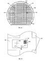
- FIG. 1A is a top view of a semiconductor wafer illustrating two common placement locations for alignment marks.
- the wafer 100 comprises a plurality of dies 110 which are delineated on the wafer by scribe lines 120.
- Alignment marks 130 can be located within an unused die.
- Alignment marks 140 can also be located within the scribe lines 120.
- scribe lines 120 have a width of less than 200 microns.
- Photolithographic tool manufacturers including ASML, SVGL, Nikon, and Canon, each require unique alignment marks and/or locations for those alignment marks. In some cases a vendor may have different marks for each of their own different photolithography tools. As a result, it is sometimes necessary for a single semiconductor wafer to have several different alignment marks.
- FIG. 1 B illustrates a partial enlarged view of wafer 100 and an alignment mark box 160 located within scribe line 120.
- Box 160 contains several different types of alignment marks 170, 180, and 190. Each of these different alignment marks could be used by a different tool in the manufacturing process.
- FIG. 2 shows a top view of a typical alignment mark 200.
- This alignment mark 200 comprises a two-dimensional grating and is similar to alignment marks used by ASML, a manufacturer of wafer steppers.
- This alignment mark further comprises four sub-gratings, 202a, 202b, 202c, and 202d.
- Sub-gratings 202a and 202d are used for alignment in the X direction, while 202b and 202c are used for alignment in the Y direction.
- FIG. 3 depicts an embodiment of a system 300 of the present invention.
- the embodiment depicted in FIG. 3 comprises a charged particle beam system 309, a host computer 342, a display 344, an operator interface 346 (such as a keyboard and mouse), memory 344, and a host interface 340.
- all or part of the functionality of host computer 301 can be replaced with one or more embedded computers.
- the workpiece 302 such as a semiconductor wafer where the alignment marks have been covered by a metallization layer, is mounted on stage 301 within vacuum chamber 305.
- Vacuum chamber 305 is evacuated by vacuum pump 318, typically to a pressure of less than 1x10⁻⁴ mbar.
- System 300 can be one of a number of stations performing specific tasks in the semiconductor manufacturing process.
- a centralized robotic arm or other automated handling system can move wafers from one station to another station under the control of a "recipe" or computer program that defines the procedures a wafer has to undergo during the manufacturing process.
- Optical microscope 306 can be used to align the workpiece 302 for determining the center of the wafer and orientation. For example, after the workpiece is in the chamber, at least three edges of a wafer can be located using the optical microscope to see the change in contrast between the wafer and no wafer. These edge locations are used to calculate the center of the wafer. The notch is then recognized and any rotation is calculated and accounted for.
- a machine vision system can be used instead of, or in addition to, the optical microscope.
- workpiece 302 can be positioned by means of a robot 303. Such robots are common in the semiconductor manufacturing process.
- workpiece 302 can be loaded into a prealignment module (not shown) which determines the orientation of the wafer, for example, by locating a notch or flat edge of the wafer.
- Automatic handler robot 303 can remove workpiece 302 from the prealignment module and place it on stage 301 so that it is properly aligned.
- workpiece 302 would be one of a batch of wafers, loaded in a wafer cassette 319 containing a number (e.g. 25 units) of wafers.
- the wafer cassette 319 and robot 303 can optionally be located inside vacuum chamber 305, or even in a secondary vacuum chamber 320.
- a cassette of wafers can loaded into a secondary vacuum chamber 320 which can then be sealed and lowered to the pressure of the main vacuum chamber 305. This reduces the need to bring the chamber up to atmospheric pressure each time a new cassette of wafers is inserted.
- Charged particle beam system 309 includes the physical hardware of the beam system, including an ion optical column 308 and a detector 304 for generating a signal corresponding to a characteristic of the surface at each point to which the beam is directed.
- Ion optical column 308 includes lenses for focusing the beam (not shown), a beam deflector 354 for steering the beam, and a beam blanker 356 for interrupting the beam, all controlled via controller 352.
- Ions are extracted from plasma ion source 310 and accelerated through ion column 308 to produce an ion beam 322, which is used to mill the metallization layer covering the alignment marks.
- the ion beam mills the surface by sputtering, that is, physically removing atoms and molecules from the specimen surface.
- Secondary electrons 324 can be collected by detector 304 to form an image of the specimen surface.
- the analog signals from detector 304 are converted into digital signals and subjected to signal processing by ion beam signal processing unit 358.
- the resulting digital signal can be used by host 342, in coordination with signals from beam deflector 354, to display an image of workpiece 301 on display 344.
- ion column 308 is a noble gas column, which produces an ion beam consisting of non-reactive, high energy ions such as argon, krypton or xenon.
- This type of column allows a usable ion beam at a much higher beam current than a typical Gallium LMIS ion column.
- a Gallium LMIS ion column normally allows a maximum beam current of around 20 nanoamps (although higher beam currents can be used, the resulting ion beam will be of very poor quality).
- a noble gas column can produce usable beam quality and current density at beam currents greater than 100 nanoamps.
- the use of a noble gas column also avoids real or perceived problems of metal contamination that may occur with a traditional Gallium ion beam.
- the beam current used would preferably be from 300 to 20,000 nanoamps, most preferably from 1500 to 5,000 nanoamps. As is well known, a higher current ion beam results in an increased sputter rate.
- the higher beam current of a noble gas column makes it possible to achieve the desired throughput requirements for mass production.
- the beam current that should be used will depend upon the material being milled and the level of accuracy required. For example, where overmilling is not an issue and endpointing is not critical, higher beam currents can be used.
- the typical alignment mark box is around 100 microns wide, some as large as 500 ⁇ m to 800 ⁇ m.
- the beam diameter may still be less than 50 ⁇ m.
- Electron Cyclotron Resonance (ECR) sources in which the plasma is generated by resonantly coupling microwave energy into the ion source
- Penning type sources in which the plasma is generated by striking a direct current discharge between a suitably shaped anode and cathode
- direct current (DC) driven volume sources in which an electric arc is struck between heated filaments and an anode
- radio frequency (RF) driven volume sources in which radio frequency energy is coupled to the gas in the ion source by a suitably configured antenna.
- the appropriate gas (such as argon, krypton, or xenon) is stored in gas storage tank 312 and introduced into plasma ion source 310 through leak valve 313.
- Leak Valve 313 can be operated manually or computer controlled via leak valve controller 350,which allows gas flow to be precisely controlled. This gas is then ionized by an appropriate energy source.
- plasma ion source 310 can be evacuated by turbomolecular pump 314 backed by a dry roughing pump (or a configuration with similar performance).
- Ions are then extracted and accelerated down through ion column 308 by the column optics (not shown).
- Ion column 308 is evacuated by turbomolecular pump 316, which is backed by roughing pump 317.
- Ion column 308 is typically maintained at a pressure of less than 1x10⁻⁶ mbar in order to maintain a gas flow appropriate for the column.
- stage 301 is a tiltable stage that can be inclined at any desired angle. Stage tilt and position can be controlled via stage controller 348.
- a tiltable stage allows ion beam 322 to be directed at workpiece 302 at an oblique angle relative to the sample surface, which results in a higher sputter rate and increased throughput.
- milling rate also referred to as sputter rate
- sputter rate typically increases with the beam angle of incidence up to a certain angle, then decreases.
- sputter rate is material dependent, typically the sputter rate is maximized where the angle of the ion beam relative to the sample surface is between 40( and 80(.
- the optimum tilt is dependent upon the material being milled and upon the sputter rate desired. For example, where endpointing is critical a lower sputter rate might be advantageous and a higher beam angle could be used.
- the ion column can be tilted instead of the stage.
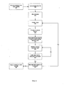
- FIG. 4 is a flowchart showing the steps of a preferred embodiment of the invention.
- a workpiece such as a semiconductor wafer where the alignment marks have been covered by a metallization layer, is retrieved from a cassette containing a number (e.g. 25 units) of wafers.
- a workpiece is loaded into a particle beam system, such as a focused ion beam, by mounting the workpiece on the FIB stage.
- the workpiece can be loaded manually or automatically, for example by an automatic handler system.
- step 412 the workpiece is aligned.
- This alignment can also be accomplished manually, for example by an operator using an optical microscope, or automatically, for example by using an automatic handler robot which locates a notch or flat edge of the wafer in order to determine the proper orientation.
- step 414 the stage is positioned so that the metallization layer covering an alignment mark is within the area scanned by the charged particle beam. This positioning can be accomplished, for example, by storing and using positional coordinates for each alignment mark to be uncovered.
- step 416 the stage is tilted to the desired angle. As discussed above, an oblique angle between the charged particle beam and the sample surface increases the milling rate.
- the appropriate beam dose required to remove the metallization layer covering the workpiece is calculated.
- Methods of calculating beam dose are well known. For example, a test layer of the same material and thickness could be experimentally milled and measured to determine the milling rate at a given beam current. The beam current and the dose required to mill away the test layer could be stored and used to mill the layer over the alignment marks on each workpiece. Because the milling rate is dependent upon the angle of incidence between a charged particle beam and a sample surface, the calculation of beam dose must take stage angle into account.
- step 420 the appropriate beam dose is applied to mill the metallization layer and uncover the alignment mark.
- step 422 adequate removal of the metallization layer is confirmed, for example by inspection with an optical microscope.
- step 424 the system determines whether any additional alignment marks on the workpiece need to be uncovered. If so, the coordinates for the next alignment mark are retrieved by the system and the process returns to step 414. The process continues until there are no further alignment marks to be uncovered.
- step 426 the completed workpiece is returned to the cassette and the next workpiece is retrieved. Once each workpiece in the cassette has been processed, the cassette is returned to the manufacturing track.
Landscapes
- Physics & Mathematics (AREA)
- General Physics & Mathematics (AREA)
- Drying Of Semiconductors (AREA)
- Container, Conveyance, Adherence, Positioning, Of Wafer (AREA)
- Exposure And Positioning Against Photoresist Photosensitive Materials (AREA)
Abstract
Description
Claims (22)
- A method for removing a material covering an alignment mark on a substrate, comprising:mounting the substrate onto a stage in a focused ion beam system, said focused ion beam system having a non-liquid metal ion source;directing an ion beam at the material covering an alignment mark, said ion beam having a beam current greater than 300 nanoamps and directed at an oblique angle relative to the surface of the substrate; andremoving said material by ion beam sputtering.
- The method of claim 1 in which the focused ion beam system has a plasma ion source.
- The method of claim 1 in which the ion beam is directed at an angle less than 80( relative to the substrate surface normal.
- A method for removing a material covering an alignment mark on a substrate, comprising:directing a charged particle beam at the material covering an alignment mark; andremoving said material by charged particle beam sputtering without using an etch assisting gas.
- The method of claim 4 in which the charged particle beam is a focused ion beam.
- The method of claim 5 in which said focused ion beam is a beam of noble gas ions.
- The method of claim 5 in which said focused ion beam is selected from the group consisting of an argon ion beam, a krypton ion beam, and a xenon ion beam.
- The method of claim 4 in which the charged particle beam is directed at an oblique angle relative to the surface of the substrate.
- The method of claim 4 in which the charged particle beam is directed at an angle of between 40( and 80( relative to the substrate surface normal.
- The method of claim 4 in which the charged particle beam has a beam current of 300 nanoamps to 20,000 nanoamps.
- The method of claim 4 in which the charged particle beam has a beam current of 1500 nanoamps to 5000 nanoamps.
- The method of claim 4 in which the substrate is a silicon wafer.
- The method of claim 4 in which the material covering an alignment mark is a metal film.
- An apparatus for removing a material covering an alignment mark on a substrate, comprising:a device for loading the substrate;a device for aligning the substrate;a device for positioning the substrate;a charged particle beam system having a charged particle source for emitting a charged particle beam, an optical system for focusing the charged particle beam, and a computer controlled beam deflector to position the charged particle beam;a device for controlling the charged particle beam dose applied to said material; anda device for unloading the substrate.
- The apparatus of claim 14 in which the charged particle beam system is a focused ion beam system.
- The apparatus of claim 14 in which the charged particle beam system is a noble gas ion beam system.
- The apparatus of claim 14 in which the charged particle beam system is selected from the group consisting of an argon ion beam system, a krypton ion beam system, and a xenon ion beam system.
- The apparatus of claim 14 in which the charged particle beam is directed at an oblique angle relative to the surface of the substrate.
- The apparatus of claim 14 in which the charged particle beam is directed at an angle of between 40( and 80( relative to the substrate surface normal.
- The apparatus of claim 14 in which the charged particle beam has a beam current of 300 nanoamps to 20,000 nanoamps.
- The apparatus of claim 14 in which the charged particle beam has a beam current of 1500 nanoamps to 5000 nanoamps.
- The apparatus of claim 14 in which the device for aligning the substrate comprises an optical microscope.
Applications Claiming Priority (2)
| Application Number | Priority Date | Filing Date | Title |
|---|---|---|---|
| US42913502P | 2002-11-26 | 2002-11-26 | |
| US429135P | 2002-11-26 |
Publications (3)
| Publication Number | Publication Date |
|---|---|
| EP1424723A2 true EP1424723A2 (en) | 2004-06-02 |
| EP1424723A3 EP1424723A3 (en) | 2009-08-05 |
| EP1424723B1 EP1424723B1 (en) | 2015-01-07 |
Family
ID=32298306
Family Applications (1)
| Application Number | Title | Priority Date | Filing Date |
|---|---|---|---|
| EP03026408.9A Expired - Lifetime EP1424723B1 (en) | 2002-11-26 | 2003-11-19 | Ion beam for target recovery |
Country Status (3)
| Country | Link |
|---|---|
| US (1) | US7150811B2 (en) |
| EP (1) | EP1424723B1 (en) |
| JP (1) | JP4943629B2 (en) |
Cited By (1)
| Publication number | Priority date | Publication date | Assignee | Title |
|---|---|---|---|---|
| FR2884045A1 (en) * | 2005-03-29 | 2006-10-06 | St Microelectronics Sa | IDENTIFICATION OF AN INTEGRATED REFERENCE CIRCUIT FOR PLUG AND POST EQUIPMENT |
Families Citing this family (12)
| Publication number | Priority date | Publication date | Assignee | Title |
|---|---|---|---|---|
| KR100898924B1 (en) * | 2002-10-24 | 2009-05-26 | 엘지전자 주식회사 | Aspheric processing method of micro lens and manufacturing method of micro lens using the same |
| US20050186753A1 (en) * | 2004-02-25 | 2005-08-25 | Ping-Hsu Chen | FIB exposure of alignment marks in MIM technology |
| JP4405865B2 (en) * | 2004-06-24 | 2010-01-27 | 富士通マイクロエレクトロニクス株式会社 | Multilayer wiring structure manufacturing method and FIB apparatus |
| KR20070101204A (en) * | 2004-08-24 | 2007-10-16 | 셀라 세미컨덕터 엔지니어링 라보라토리스 리미티드 | Methods, apparatus, and systems for applying, deflecting, deflecting and controlling the extent of an ion beam to mill a workpiece |
| JP4216263B2 (en) * | 2005-03-09 | 2009-01-28 | シャープ株式会社 | Manufacturing inspection analysis system and manufacturing inspection analysis method |
| DE102008000709B3 (en) * | 2008-03-17 | 2009-11-26 | Carl Zeiss Smt Ag | Cleaning module, EUV lithography apparatus and method for its cleaning |
| DE112011103677B4 (en) | 2010-11-05 | 2017-10-05 | Hitachi High-Technologies Corporation | ion etching |
| US9190261B2 (en) * | 2011-08-25 | 2015-11-17 | Taiwan Semiconductor Manufacturing Company, Ltd. | Layer alignment in FinFET fabrication |
| EP2787523B1 (en) * | 2013-04-03 | 2016-02-10 | Fei Company | Low energy ion milling or deposition |
| WO2016121079A1 (en) * | 2015-01-30 | 2016-08-04 | 株式会社 日立ハイテクノロジーズ | Electron microscope equipped with ion milling device, and three-dimensional reconstruction method |
| EP3249676B1 (en) | 2016-05-27 | 2018-10-03 | FEI Company | Dual-beam charged-particle microscope with in situ deposition functionality |
| ES3010110B2 (en) * | 2023-09-29 | 2025-12-18 | Consejo Superior Investigacion | ELECTRICAL CONTACT MANUFACTURING SYSTEM AND ASSOCIATED MANUFACTURING METHOD |
Family Cites Families (44)
| Publication number | Priority date | Publication date | Assignee | Title |
|---|---|---|---|---|
| US3699334A (en) * | 1969-06-16 | 1972-10-17 | Kollsman Instr Corp | Apparatus using a beam of positive ions for controlled erosion of surfaces |
| US3860783A (en) | 1970-10-19 | 1975-01-14 | Bell Telephone Labor Inc | Ion etching through a pattern mask |
| DE2603675A1 (en) | 1976-01-31 | 1977-08-04 | Leybold Heraeus Gmbh & Co Kg | METHOD OF CONTROLLING THE REMOVAL OF A THIN LAYER OR THROUGH MASKING OF SPECIFIC AREAS OF THE LAYER WITH THE HELP OF ION ETCHING |
| JPS5562734A (en) | 1978-11-01 | 1980-05-12 | Toshiba Corp | Ion source and ion etching method |
| JPS5694630A (en) * | 1979-12-27 | 1981-07-31 | Nec Corp | Etching method using ion-beam |
| JPS56107555A (en) * | 1980-01-29 | 1981-08-26 | Nec Corp | Detection of position of electron beam |
| US4490210A (en) | 1984-01-24 | 1984-12-25 | International Business Machines Corporation | Laser induced dry chemical etching of metals |
| JPH01225772A (en) * | 1988-03-04 | 1989-09-08 | Nippon Telegr & Teleph Corp <Ntt> | Ion beam sputtering device |
| US5643472A (en) | 1988-07-08 | 1997-07-01 | Cauldron Limited Partnership | Selective removal of material by irradiation |
| US5018164A (en) | 1989-09-12 | 1991-05-21 | Hughes Aircraft Company | Excimer laser ablation method and apparatus for microcircuit fabrication |
| US4975141A (en) | 1990-03-30 | 1990-12-04 | International Business Machines Corporation | Laser ablation for plasma etching endpoint detection |
| EP0477154B1 (en) | 1990-09-04 | 1994-03-09 | Lift And Go Products Aktiebolag | Load handling device with extendable load engaging members |
| JPH053143A (en) | 1991-04-19 | 1993-01-08 | Hitachi Ltd | Alignment method and device |
| JP3349519B2 (en) * | 1992-02-04 | 2002-11-25 | 株式会社日立製作所 | Sputtering equipment |
| US5807650A (en) * | 1992-03-24 | 1998-09-15 | Kabushiki Kaisha Toshiba | Photo mask and apparatus for repairing photo mask |
| JP3117836B2 (en) * | 1993-03-02 | 2000-12-18 | セイコーインスツルメンツ株式会社 | Focused ion beam equipment |
| US5504340A (en) * | 1993-03-10 | 1996-04-02 | Hitachi, Ltd. | Process method and apparatus using focused ion beam generating means |
| US5483037A (en) | 1993-12-01 | 1996-01-09 | Martin Marietta Energy Systems, Inc. | Multiple target laser ablation system |
| US5456756A (en) | 1994-09-02 | 1995-10-10 | Advanced Micro Devices, Inc. | Holding apparatus, a metal deposition system, and a wafer processing method which preserve topographical marks on a semiconductor wafer |
| US5952247A (en) | 1994-11-23 | 1999-09-14 | Intel Corporation | Method of accessing the circuitry on a semiconductor substrate from the bottom of the semiconductor substrate |
| US6057525A (en) | 1995-09-05 | 2000-05-02 | United States Enrichment Corporation | Method and apparatus for precision laser micromachining |
| TW350095B (en) | 1995-11-21 | 1999-01-11 | Daido Hoxan Inc | Cutting method and apparatus for semiconductor materials |
| WO1998020534A1 (en) | 1996-11-08 | 1998-05-14 | W.L. Gore & Associates, Inc. | Method for using fiducial schemes to increase nominal registration |
| US5911108A (en) | 1997-01-29 | 1999-06-08 | Integrated Device Technology, Inc. | Method for protecting an alignment mark on a semiconductor substrate during chemical mechanical polishing and the resulting structure |
| US5738961A (en) | 1997-03-03 | 1998-04-14 | Taiwan Semiconductor Manufacturing Company, Ltd. | Two-step photolithography method for aligning and patterning non-transparent layers |
| US6083841A (en) | 1997-05-15 | 2000-07-04 | Rohm Co., Ltd. | Method of etching gallium-nitride based compound semiconductor layer and method of manufacturing semiconductor light emitting device utilizing the same |
| JPH11238209A (en) * | 1998-02-23 | 1999-08-31 | Yamaha Corp | Method for manufacturing thin-film magnetic head |
| JP2000021978A (en) | 1998-07-03 | 2000-01-21 | Mitsubishi Electric Corp | Photomask and pattern forming method |
| JP2000035390A (en) * | 1998-07-16 | 2000-02-02 | Seiko Instruments Inc | Sectioning method |
| US6268608B1 (en) | 1998-10-09 | 2001-07-31 | Fei Company | Method and apparatus for selective in-situ etching of inter dielectric layers |
| US6288773B2 (en) | 1998-12-11 | 2001-09-11 | Lsi Logic Corporation | Method and apparatus for removing residual material from an alignment mark of a semiconductor wafer |
| US6440615B1 (en) * | 1999-02-09 | 2002-08-27 | Nikon Corporation | Method of repairing a mask with high electron scattering and low electron absorption properties |
| US6277659B1 (en) | 1999-09-29 | 2001-08-21 | Advanced Micro Devices, Inc. | Substrate removal using thermal analysis |
| US6261918B1 (en) | 1999-10-04 | 2001-07-17 | Conexant Systems, Inc. | Method for creating and preserving alignment marks for aligning mask layers in integrated circuit manufacture |
| US6281471B1 (en) | 1999-12-28 | 2001-08-28 | Gsi Lumonics, Inc. | Energy-efficient, laser-based method and system for processing target material |
| US6552301B2 (en) | 2000-01-25 | 2003-04-22 | Peter R. Herman | Burst-ultrafast laser machining method |
| US6322672B1 (en) * | 2000-03-10 | 2001-11-27 | Fei Company | Method and apparatus for milling copper interconnects in a charged particle beam system |
| JP2001345360A (en) * | 2000-06-01 | 2001-12-14 | Hitachi Ltd | Inspection / analysis method and sample preparation device |
| JP4178741B2 (en) * | 2000-11-02 | 2008-11-12 | 株式会社日立製作所 | Charged particle beam apparatus and sample preparation apparatus |
| JP4354657B2 (en) * | 2001-01-11 | 2009-10-28 | エスアイアイ・ナノテクノロジー株式会社 | Focused ion beam device |
| JP4127601B2 (en) * | 2001-03-09 | 2008-07-30 | 株式会社東芝 | Laser processing equipment |
| JPWO2002075806A1 (en) * | 2001-03-16 | 2004-07-08 | 株式会社日立製作所 | Wafer inspection method, focused ion beam device, and transmitted electron beam device |
| JP2002280295A (en) * | 2001-03-22 | 2002-09-27 | Sony Corp | Semiconductor element manufacturing method and imaging element manufacturing method |
| US20030138709A1 (en) * | 2001-11-09 | 2003-07-24 | Burbank Daniel P. | Wafer fabrication having improved laserwise alignment recovery |
-
2003
- 2003-09-24 US US10/669,616 patent/US7150811B2/en not_active Expired - Lifetime
- 2003-11-19 EP EP03026408.9A patent/EP1424723B1/en not_active Expired - Lifetime
- 2003-11-26 JP JP2003396297A patent/JP4943629B2/en not_active Expired - Fee Related
Cited By (3)
| Publication number | Priority date | Publication date | Assignee | Title |
|---|---|---|---|---|
| FR2884045A1 (en) * | 2005-03-29 | 2006-10-06 | St Microelectronics Sa | IDENTIFICATION OF AN INTEGRATED REFERENCE CIRCUIT FOR PLUG AND POST EQUIPMENT |
| US7629186B2 (en) | 2005-03-29 | 2009-12-08 | Stmicroelectronics Sa | System and method for identification of a reference integrated circuit for a pick-and-place equipment |
| EP1708250A3 (en) * | 2005-03-29 | 2011-08-24 | St Microelectronics S.A. | Identification of a reference integrated circuit for a pick and place device |
Also Published As
| Publication number | Publication date |
|---|---|
| JP4943629B2 (en) | 2012-05-30 |
| EP1424723B1 (en) | 2015-01-07 |
| US20040099638A1 (en) | 2004-05-27 |
| JP2004179165A (en) | 2004-06-24 |
| EP1424723A3 (en) | 2009-08-05 |
| US7150811B2 (en) | 2006-12-19 |
Similar Documents
| Publication | Publication Date | Title |
|---|---|---|
| EP1261752B1 (en) | Method for repairing lithography masks using a charged particle beam system | |
| US7504182B2 (en) | Photolithography mask repair | |
| US8835845B2 (en) | In-situ STEM sample preparation | |
| US6753538B2 (en) | Electron beam processing | |
| US7150811B2 (en) | Ion beam for target recovery | |
| WO1999028220A1 (en) | Substrate transferring device and method | |
| JP2001144013A (en) | Lithographic projection equipment | |
| JPH053143A (en) | Alignment method and device | |
| JP4279369B2 (en) | Semiconductor device processing method | |
| US6933081B2 (en) | Method for quartz bump defect repair with less substrate damage | |
| JP3218984B2 (en) | Wafer periphery exposure method and apparatus for removing unnecessary resist on semiconductor wafer | |
| KR20230033926A (en) | Apparatus for treating substrate and method for processing a substrate | |
| US7374866B2 (en) | System and method for exposure of partial edge die | |
| US7045019B1 (en) | Method for performing site-specific backside particle and contamination removal | |
| US20020127865A1 (en) | Lithography method for forming semiconductor devices with sub-micron structures on a wafer and apparatus | |
| JP2888228B2 (en) | Structure of partial mask for charged particle beam | |
| US20010031404A1 (en) | Process for fabricating a projection electron lithography mask and a removable, reusable cover for use therein | |
| CN116364597A (en) | Substrate processing equipment and substrate processing method | |
| CN117594427A (en) | A method to improve the clarity of laser marked areas | |
| JP2003332226A (en) | Mask defect repair method and mask manufacturing method | |
| JP2005136284A (en) | Exposure method and exposure apparatus | |
| HK1029663A (en) | Pattern film repair using a gas assisted focused particle beam system |
Legal Events
| Date | Code | Title | Description |
|---|---|---|---|
| PUAI | Public reference made under article 153(3) epc to a published international application that has entered the european phase |
Free format text: ORIGINAL CODE: 0009012 |
|
| 17P | Request for examination filed |
Effective date: 20031119 |
|
| AK | Designated contracting states |
Kind code of ref document: A2 Designated state(s): AT BE BG CH CY CZ DE DK EE ES FI FR GB GR HU IE IT LI LU MC NL PT RO SE SI SK TR |
|
| AX | Request for extension of the european patent |
Extension state: AL LT LV MK |
|
| RIC1 | Information provided on ipc code assigned before grant |
Ipc: H01L 21/00 20060101AFI20040413BHEP Ipc: H01L 23/544 20060101ALI20090130BHEP Ipc: H01L 21/02 20060101ALI20090130BHEP Ipc: H01L 21/3213 20060101ALI20090130BHEP Ipc: G03F 9/00 20060101ALI20090130BHEP |
|
| PUAL | Search report despatched |
Free format text: ORIGINAL CODE: 0009013 |
|
| AK | Designated contracting states |
Kind code of ref document: A3 Designated state(s): AT BE BG CH CY CZ DE DK EE ES FI FR GB GR HU IE IT LI LU MC NL PT RO SE SI SK TR |
|
| AX | Request for extension of the european patent |
Extension state: AL LT LV MK |
|
| RIC1 | Information provided on ipc code assigned before grant |
Ipc: H01L 21/027 20060101ALI20090629BHEP Ipc: H01L 21/02 20060101ALI20090629BHEP Ipc: H01L 21/3213 20060101ALI20090629BHEP Ipc: G03F 9/00 20060101ALI20090629BHEP Ipc: H01L 21/00 20060101AFI20040413BHEP Ipc: H01L 23/544 20060101ALI20090629BHEP |
|
| AKX | Designation fees paid |
Designated state(s): AT BE BG CH CY CZ DE DK EE ES FI FR GB GR HU IE IT LI LU MC NL PT RO SE SI SK TR |
|
| 17Q | First examination report despatched |
Effective date: 20110614 |
|
| REG | Reference to a national code |
Ref country code: DE Ref legal event code: R079 Ref document number: 60347191 Country of ref document: DE Free format text: PREVIOUS MAIN CLASS: H01L0021000000 Ipc: H01L0021020000 |
|
| GRAP | Despatch of communication of intention to grant a patent |
Free format text: ORIGINAL CODE: EPIDOSNIGR1 |
|
| RIC1 | Information provided on ipc code assigned before grant |
Ipc: H01L 21/67 20060101ALI20140902BHEP Ipc: G03F 9/00 20060101ALI20140902BHEP Ipc: H01L 21/02 20060101AFI20140902BHEP Ipc: H01L 23/544 20060101ALI20140902BHEP Ipc: H01L 21/68 20060101ALI20140902BHEP Ipc: H01L 21/3213 20060101ALI20140902BHEP |
|
| INTG | Intention to grant announced |
Effective date: 20140917 |
|
| GRAS | Grant fee paid |
Free format text: ORIGINAL CODE: EPIDOSNIGR3 |
|
| GRAA | (expected) grant |
Free format text: ORIGINAL CODE: 0009210 |
|
| AK | Designated contracting states |
Kind code of ref document: B1 Designated state(s): AT BE BG CH CY CZ DE DK EE ES FI FR GB GR HU IE IT LI LU MC NL PT RO SE SI SK TR |
|
| REG | Reference to a national code |
Ref country code: GB Ref legal event code: FG4D |
|
| REG | Reference to a national code |
Ref country code: CH Ref legal event code: EP |
|
| REG | Reference to a national code |
Ref country code: IE Ref legal event code: FG4D |
|
| REG | Reference to a national code |
Ref country code: AT Ref legal event code: REF Ref document number: 706259 Country of ref document: AT Kind code of ref document: T Effective date: 20150215 |
|
| REG | Reference to a national code |
Ref country code: DE Ref legal event code: R096 Ref document number: 60347191 Country of ref document: DE Effective date: 20150226 |
|
| REG | Reference to a national code |
Ref country code: NL Ref legal event code: VDEP Effective date: 20150107 |
|
| REG | Reference to a national code |
Ref country code: AT Ref legal event code: MK05 Ref document number: 706259 Country of ref document: AT Kind code of ref document: T Effective date: 20150107 |
|
| PG25 | Lapsed in a contracting state [announced via postgrant information from national office to epo] |
Ref country code: FI Free format text: LAPSE BECAUSE OF FAILURE TO SUBMIT A TRANSLATION OF THE DESCRIPTION OR TO PAY THE FEE WITHIN THE PRESCRIBED TIME-LIMIT Effective date: 20150107 Ref country code: ES Free format text: LAPSE BECAUSE OF FAILURE TO SUBMIT A TRANSLATION OF THE DESCRIPTION OR TO PAY THE FEE WITHIN THE PRESCRIBED TIME-LIMIT Effective date: 20150107 Ref country code: SE Free format text: LAPSE BECAUSE OF FAILURE TO SUBMIT A TRANSLATION OF THE DESCRIPTION OR TO PAY THE FEE WITHIN THE PRESCRIBED TIME-LIMIT Effective date: 20150107 Ref country code: BG Free format text: LAPSE BECAUSE OF FAILURE TO SUBMIT A TRANSLATION OF THE DESCRIPTION OR TO PAY THE FEE WITHIN THE PRESCRIBED TIME-LIMIT Effective date: 20150407 |
|
| PG25 | Lapsed in a contracting state [announced via postgrant information from national office to epo] |
Ref country code: NL Free format text: LAPSE BECAUSE OF FAILURE TO SUBMIT A TRANSLATION OF THE DESCRIPTION OR TO PAY THE FEE WITHIN THE PRESCRIBED TIME-LIMIT Effective date: 20150107 Ref country code: GR Free format text: LAPSE BECAUSE OF FAILURE TO SUBMIT A TRANSLATION OF THE DESCRIPTION OR TO PAY THE FEE WITHIN THE PRESCRIBED TIME-LIMIT Effective date: 20150408 Ref country code: AT Free format text: LAPSE BECAUSE OF FAILURE TO SUBMIT A TRANSLATION OF THE DESCRIPTION OR TO PAY THE FEE WITHIN THE PRESCRIBED TIME-LIMIT Effective date: 20150107 |
|
| REG | Reference to a national code |
Ref country code: DE Ref legal event code: R097 Ref document number: 60347191 Country of ref document: DE |
|
| PG25 | Lapsed in a contracting state [announced via postgrant information from national office to epo] |
Ref country code: CZ Free format text: LAPSE BECAUSE OF FAILURE TO SUBMIT A TRANSLATION OF THE DESCRIPTION OR TO PAY THE FEE WITHIN THE PRESCRIBED TIME-LIMIT Effective date: 20150107 Ref country code: SK Free format text: LAPSE BECAUSE OF FAILURE TO SUBMIT A TRANSLATION OF THE DESCRIPTION OR TO PAY THE FEE WITHIN THE PRESCRIBED TIME-LIMIT Effective date: 20150107 Ref country code: EE Free format text: LAPSE BECAUSE OF FAILURE TO SUBMIT A TRANSLATION OF THE DESCRIPTION OR TO PAY THE FEE WITHIN THE PRESCRIBED TIME-LIMIT Effective date: 20150107 Ref country code: RO Free format text: LAPSE BECAUSE OF FAILURE TO SUBMIT A TRANSLATION OF THE DESCRIPTION OR TO PAY THE FEE WITHIN THE PRESCRIBED TIME-LIMIT Effective date: 20150107 Ref country code: DK Free format text: LAPSE BECAUSE OF FAILURE TO SUBMIT A TRANSLATION OF THE DESCRIPTION OR TO PAY THE FEE WITHIN THE PRESCRIBED TIME-LIMIT Effective date: 20150107 |
|
| PLBE | No opposition filed within time limit |
Free format text: ORIGINAL CODE: 0009261 |
|
| STAA | Information on the status of an ep patent application or granted ep patent |
Free format text: STATUS: NO OPPOSITION FILED WITHIN TIME LIMIT |
|
| REG | Reference to a national code |
Ref country code: FR Ref legal event code: PLFP Year of fee payment: 13 |
|
| 26N | No opposition filed |
Effective date: 20151008 |
|
| PG25 | Lapsed in a contracting state [announced via postgrant information from national office to epo] |
Ref country code: IT Free format text: LAPSE BECAUSE OF FAILURE TO SUBMIT A TRANSLATION OF THE DESCRIPTION OR TO PAY THE FEE WITHIN THE PRESCRIBED TIME-LIMIT Effective date: 20150107 |
|
| PG25 | Lapsed in a contracting state [announced via postgrant information from national office to epo] |
Ref country code: SI Free format text: LAPSE BECAUSE OF FAILURE TO SUBMIT A TRANSLATION OF THE DESCRIPTION OR TO PAY THE FEE WITHIN THE PRESCRIBED TIME-LIMIT Effective date: 20150107 |
|
| PG25 | Lapsed in a contracting state [announced via postgrant information from national office to epo] |
Ref country code: BE Free format text: LAPSE BECAUSE OF FAILURE TO SUBMIT A TRANSLATION OF THE DESCRIPTION OR TO PAY THE FEE WITHIN THE PRESCRIBED TIME-LIMIT Effective date: 20150107 |
|
| PG25 | Lapsed in a contracting state [announced via postgrant information from national office to epo] |
Ref country code: MC Free format text: LAPSE BECAUSE OF FAILURE TO SUBMIT A TRANSLATION OF THE DESCRIPTION OR TO PAY THE FEE WITHIN THE PRESCRIBED TIME-LIMIT Effective date: 20150107 Ref country code: LU Free format text: LAPSE BECAUSE OF FAILURE TO SUBMIT A TRANSLATION OF THE DESCRIPTION OR TO PAY THE FEE WITHIN THE PRESCRIBED TIME-LIMIT Effective date: 20151119 |
|
| REG | Reference to a national code |
Ref country code: CH Ref legal event code: PL |
|
| PG25 | Lapsed in a contracting state [announced via postgrant information from national office to epo] |
Ref country code: CH Free format text: LAPSE BECAUSE OF NON-PAYMENT OF DUE FEES Effective date: 20151130 Ref country code: LI Free format text: LAPSE BECAUSE OF NON-PAYMENT OF DUE FEES Effective date: 20151130 |
|
| REG | Reference to a national code |
Ref country code: IE Ref legal event code: MM4A |
|
| PG25 | Lapsed in a contracting state [announced via postgrant information from national office to epo] |
Ref country code: IE Free format text: LAPSE BECAUSE OF NON-PAYMENT OF DUE FEES Effective date: 20151119 |
|
| REG | Reference to a national code |
Ref country code: FR Ref legal event code: PLFP Year of fee payment: 14 |
|
| PG25 | Lapsed in a contracting state [announced via postgrant information from national office to epo] |
Ref country code: HU Free format text: LAPSE BECAUSE OF FAILURE TO SUBMIT A TRANSLATION OF THE DESCRIPTION OR TO PAY THE FEE WITHIN THE PRESCRIBED TIME-LIMIT; INVALID AB INITIO Effective date: 20031119 |
|
| PG25 | Lapsed in a contracting state [announced via postgrant information from national office to epo] |
Ref country code: CY Free format text: LAPSE BECAUSE OF FAILURE TO SUBMIT A TRANSLATION OF THE DESCRIPTION OR TO PAY THE FEE WITHIN THE PRESCRIBED TIME-LIMIT Effective date: 20150107 |
|
| PG25 | Lapsed in a contracting state [announced via postgrant information from national office to epo] |
Ref country code: TR Free format text: LAPSE BECAUSE OF FAILURE TO SUBMIT A TRANSLATION OF THE DESCRIPTION OR TO PAY THE FEE WITHIN THE PRESCRIBED TIME-LIMIT Effective date: 20150107 |
|
| REG | Reference to a national code |
Ref country code: FR Ref legal event code: PLFP Year of fee payment: 15 |
|
| PGFP | Annual fee paid to national office [announced via postgrant information from national office to epo] |
Ref country code: FR Payment date: 20171012 Year of fee payment: 15 Ref country code: DE Payment date: 20171114 Year of fee payment: 15 |
|
| PGFP | Annual fee paid to national office [announced via postgrant information from national office to epo] |
Ref country code: GB Payment date: 20171115 Year of fee payment: 15 |
|
| PG25 | Lapsed in a contracting state [announced via postgrant information from national office to epo] |
Ref country code: PT Free format text: LAPSE BECAUSE OF FAILURE TO SUBMIT A TRANSLATION OF THE DESCRIPTION OR TO PAY THE FEE WITHIN THE PRESCRIBED TIME-LIMIT Effective date: 20150107 |
|
| REG | Reference to a national code |
Ref country code: DE Ref legal event code: R119 Ref document number: 60347191 Country of ref document: DE |
|
| GBPC | Gb: european patent ceased through non-payment of renewal fee |
Effective date: 20181119 |
|
| PG25 | Lapsed in a contracting state [announced via postgrant information from national office to epo] |
Ref country code: FR Free format text: LAPSE BECAUSE OF NON-PAYMENT OF DUE FEES Effective date: 20181130 Ref country code: DE Free format text: LAPSE BECAUSE OF NON-PAYMENT OF DUE FEES Effective date: 20190601 |
|
| PG25 | Lapsed in a contracting state [announced via postgrant information from national office to epo] |
Ref country code: GB Free format text: LAPSE BECAUSE OF NON-PAYMENT OF DUE FEES Effective date: 20181119 |