EP1424688A2 - Spin valve head and magnetic recording device using the same - Google Patents
Spin valve head and magnetic recording device using the same Download PDFInfo
- Publication number
- EP1424688A2 EP1424688A2 EP03257427A EP03257427A EP1424688A2 EP 1424688 A2 EP1424688 A2 EP 1424688A2 EP 03257427 A EP03257427 A EP 03257427A EP 03257427 A EP03257427 A EP 03257427A EP 1424688 A2 EP1424688 A2 EP 1424688A2
- Authority
- EP
- European Patent Office
- Prior art keywords
- layer
- spin valve
- valve head
- magnetic layer
- pinned
- Prior art date
- Legal status (The legal status is an assumption and is not a legal conclusion. Google has not performed a legal analysis and makes no representation as to the accuracy of the status listed.)
- Withdrawn
Links
Images


Classifications
-
- G—PHYSICS
- G11—INFORMATION STORAGE
- G11B—INFORMATION STORAGE BASED ON RELATIVE MOVEMENT BETWEEN RECORD CARRIER AND TRANSDUCER
- G11B5/00—Recording by magnetisation or demagnetisation of a record carrier; Reproducing by magnetic means; Record carriers therefor
- G11B5/127—Structure or manufacture of heads, e.g. inductive
- G11B5/33—Structure or manufacture of flux-sensitive heads, i.e. for reproduction only; Combination of such heads with means for recording or erasing only
- G11B5/39—Structure or manufacture of flux-sensitive heads, i.e. for reproduction only; Combination of such heads with means for recording or erasing only using magneto-resistive devices or effects
- G11B5/3903—Structure or manufacture of flux-sensitive heads, i.e. for reproduction only; Combination of such heads with means for recording or erasing only using magneto-resistive devices or effects using magnetic thin film layers or their effects, the films being part of integrated structures
-
- B—PERFORMING OPERATIONS; TRANSPORTING
- B82—NANOTECHNOLOGY
- B82Y—SPECIFIC USES OR APPLICATIONS OF NANOSTRUCTURES; MEASUREMENT OR ANALYSIS OF NANOSTRUCTURES; MANUFACTURE OR TREATMENT OF NANOSTRUCTURES
- B82Y10/00—Nanotechnology for information processing, storage or transmission, e.g. quantum computing or single electron logic
-
- B—PERFORMING OPERATIONS; TRANSPORTING
- B82—NANOTECHNOLOGY
- B82Y—SPECIFIC USES OR APPLICATIONS OF NANOSTRUCTURES; MEASUREMENT OR ANALYSIS OF NANOSTRUCTURES; MANUFACTURE OR TREATMENT OF NANOSTRUCTURES
- B82Y25/00—Nanomagnetism, e.g. magnetoimpedance, anisotropic magnetoresistance, giant magnetoresistance or tunneling magnetoresistance
-
- G—PHYSICS
- G11—INFORMATION STORAGE
- G11B—INFORMATION STORAGE BASED ON RELATIVE MOVEMENT BETWEEN RECORD CARRIER AND TRANSDUCER
- G11B5/00—Recording by magnetisation or demagnetisation of a record carrier; Reproducing by magnetic means; Record carriers therefor
- G11B5/127—Structure or manufacture of heads, e.g. inductive
- G11B5/33—Structure or manufacture of flux-sensitive heads, i.e. for reproduction only; Combination of such heads with means for recording or erasing only
- G11B5/39—Structure or manufacture of flux-sensitive heads, i.e. for reproduction only; Combination of such heads with means for recording or erasing only using magneto-resistive devices or effects
- G11B2005/3996—Structure or manufacture of flux-sensitive heads, i.e. for reproduction only; Combination of such heads with means for recording or erasing only using magneto-resistive devices or effects large or giant magnetoresistive effects [GMR], e.g. as generated in spin-valve [SV] devices
Definitions
- the present invention relates to a spin valve head and a magnetic recording device using the spin valve head.
- a Magneto-Resistive (MR) head which detects variations of signal magnetic fields in a magnetic recording medium as variations of electrical resistivity, is used as a reproducing head.
- a rate of changing electric resistance (MR-ratio) of a spin valve head is greater than that of a conventional MR element, so the spin valve head is used as an MR element for great surface recording density.
- a previously-proposed spin valve head has a spin valve film, in which an antiferromagnetic layer, a pinned magnetic layer (a fixed magnetic layer), an intermediate layer, a free layer, etc. are piled, and electrodes are formed on the both sides of the spin valve film. An electric current runs in parallel to a surface of the spin valve film.
- This spin valve head called a CIP (Current In Plane) type is mainly used.
- a synthetic ferrimagnet spin valve head in which an electric current runs perpendicular to the surface of the spin valve film, is used.
- the spin valve film of the synthetic ferrimagnet spin valve head is shown in Fig. 2.
- an antiferomagnetic layer 12 a first pinned magnetic layer 141, a non-magnetic layer 15 made of, for example, ruthenium, a second pinned magnetic layer 142, an intermediate layer 16, a free layer 18 and a gap layer 20 are piled on a base layer 10 in that order.
- Magnetizing directions of the first pinned magnetic layer 141 and the second pinned magnetic layer 142 are mutually opposite.
- the non-magnetic layer 15 exchange-couples the first pinned magnetic layer 141 with the second pinned magnetic layer 142.
- the second pinned magnetic layer 142 includes a pinned-2A layer 142a and a pinned-2B layer 142b, and a specular layer 143 is formed between the pinned-2A layer 142a and the pinned-2B layer 142b.
- the specular layer 143 specular-reflects electrons on a boundary face between a metal and an insulator so as to make magnetic resistance greater (see Japanese Patent Publication No. 2000-252548).
- Magnetic characteristics of the spin valve film having the specular layer 143 shown in Fig. 2 are highly influenced by thickness of the the pinned-2A layer 142a and the pinned-2B layer 142b.
- Fig. 5 Variations of the MR-ratio and one way anisotropy field (Hua values) with respect to thickness of the second pinned magnetic layer 142 are shown in Fig. 5. Note that, thickness of the first pinned magnetic layer 141 was 1.2 nm; thickness of the pinned-2A layer 142a was 0.9 nm; and thickness of the pinned-2B layer 142b was 1.3 nm; the firs pinned magnetic layer 141 was made of CoFe and had thickness of 1.2 nm; thickness of the non-magnetic layer 15 was 0.85 nm; the intermediate layer was made of Cu and had thickness of 2.2 nm; and the free magnetic layer included a CoFe layer having thickness of 0.5 nm and a CoNiFe layer having thickness of 2.16nm.
- Total thickness of the second pinned magnetic layer 142 was the sum of the thickness of the pinned-2A layer 142a and the thickness of the pinned-2B layer 142B.
- the thickness of the pinned-2A layer 142a was fixed to 0.9 nm, and the total thickness of the second pinned magnetic layer 142 was varied;
- the thickness of the pinned-2B layer 142b was fixed to 1.3 nm, and the total thickness of the second pinned magnetic layer 142 was varied.
- the MR-ratio slightly increased with increasing the total thickness of the second pinned magnetic layer 142.
- the Hua reduced relatively fast with increasing the total thickness of the second pinned magnetic layer 142.
- the Hua reduced faster when the thickness of the pinned-2B layer 142b was fixed and the thickness of the pinned-2A layer 142 was made thicker. Therefore, the results teaches that making the pinned-2A layer 142a thin and making the pinned-2B layer 142b thick are effective to increase the MR-ratio and the Hua values.
- spin valve head which is capable of having a secure specular effect, increasing MR-ratio and Hua and outputting a prescribed head power when the head accesses a recording medium having high surface recording density.
- the spin valve head of one embodiment of the present invention has the following structures.
- the spin valve head comprises: a first pinned magnetic layer; a non-magnetic layer being formed on the first pinned magnetic layer; and a second pinned magnetic layer being formed on the non-magnetic layer, and is characterized by an insulating specular layer being provided between the first pinned magnetic layer and the second pinned magnetic layer.
- the insulating specular layer may be provided between the non-magnetic layer and the second pinned magnetic layer.
- the insulating specular layer may be made of an oxide of an alloy including at least one of Co, Ni and Fe.
- thickness of the insulating specular layer may be 0.6-1.0 nm.
- the insulating specular layer may be an oxide film, which is formed by oxidizing a metal layer.
- the metal layer is oxidized by a process selected from natural oxidization, plasma oxidization and ion beam oxidization.
- the insulating specular layer may be a metal oxide film formed, on the non-magnetic layer, by a film forming process.
- the film forming process is selected from spattering, evaporation and CVD (Chemical Vapor Deposition).
- the insulating specular layer may be formed by forming a film of the oxide on the non-magnetic layer in a chamber and introducing oxygen into the chamber to stick oxygen onto a surface of the non-magnetic oxide film.
- a magnetic recording device embodying the present invention has a magnetic head section for reproducing data recorded on a magnetic recording medium, and the magnetic head section preferably includes the spin valve head described above.
- a spin valve head embodying the present invention can be used as a magnetic head element having good MR-ratio and Hua value.
- the magnetic head element has superior and stable characteristics.
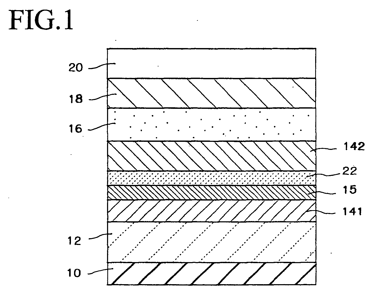
- Fig. 1 is a schematic view showing a constitution of a spin valve head of an embodiment of the present invention.
- a base layer 10 is formed on a substrate, e.g., a ceramic wafer.
- the base layer 10 of the present invention is made of NiCr.
- the base layer 10 is formed by a proper film forming process, e.g., spattering, evaporation, CVD (Chemical Vapor Deposition).
- An antiferromagnetic layer 12 is formed on the base layer 10.
- the antiferromagnetic layer 12 acts as a layer for applying an exchange bias magnetic field, and it is made of an antiferromagnetic material, e.g., PtMn, PdPtMn.
- the antiferromagnetic layer 12 is also formed by a proper film forming process, e.g., spattering, evaporation, CVD.
- a first pinned (sandwiched) magnetic layer 141 is formed on the antiferromagnetic layer 12.
- An insulating specular layer 22 is formed on the non-magnetic layer 15.
- a second pinned magnetic layer 142 is formed on the specular layer 15. Magnetizing directions of the first pinned magnetic layer 141 and the second pinned magnetic layer 142 are fixed and mutually opposite.
- the first pinned magnetic layer 141 and the second pinned magnetic layer 142 are made of a ferromagnetic material, e.g., CoFe alloy, CoFeB alloy.
- the first pinned magnetic layer 141 and the second pinned magnetic layer 142 are formed by a proper film forming process, e.g., spattering, evaporation, CVD. Thickness of the first pinned magnetic layer 141 and the second pinned magnetic layer 142 may be optionally selected. In the present embodiment, their thickness are 1-2 nm.
- the non-magnetic layer 15 acts as an exchange coupling layer between the first pinned magnetic layer 141 and the second pinned magnetic layer 142.
- the non-magnetic layer 15 is formed on the first pinned magnetic layer 141 by a proper film forming process, e.g., spattering (sputtering), evaporation, CVD.
- a feature of the spin valve film of the present embodiment is the insulating specular layer 22 formed on the non-magnetic layer 15.
- the insulating specular layer 22 is made of an oxide and formed on the non-magnetic layer 15 as an insulating layer.
- a metal layer which is made of a metal, e.g., Co, Ni, Fe, or an alloy, e.g., CoNiFe, is formed on the non-magnetic layer 15 by a proper film forming process, e.g., spattering, evaporation, CVD.
- the metal layer is oxidized, by a proper oxidization process, e.g., natural oxidization, plasma oxidization, ion beam oxidization, so as to form an oxide film.
- a proper oxidization process e.g., natural oxidization, plasma oxidization, ion beam oxidization
- an oxide of a metal e.g., Co, Ni, Fe, or an alloy, e.g., CoNiFe
- a proper film forming process e.g., spattering, evaporation, CVD.
- the insulating specular layer 22 is formed by forming the oxide film on the non-magnetic layer 15 in a film forming chamber, then oxygen is introduced into the chamber to stick oxygen onto a surface of the insulating specular layer 22.
- the second pinned magnetic layer 142 is formed on the insulating specular layer 22 by a proper film forming process, e.g., spattering, evaporation, CVD.
- the second pinned magnetic layer 142 includes two sub-layers: the pinned-2A layer 142a and the pinned-2B layer 142b.
- the second pinned layer 142 is a single layer. This is another feature of the present embodiment.
- an intermediate layer 16 is an insulating layer.
- the intermediate layer 16 is made of a non-magnetic material, e.g., Cu.
- the intermediate layer 16 is also formed by a proper film forming process, e.g., spattering, evaporation, CVD.
- a free magnetic layer 18 is made of a soft magnetic material, e.g., CoFe alloy, CoFeB alloy.
- the free magnetic layer 18 may be a single layer and may include a plurality of sub-layers.
- the free layer 18 is also formed by a proper film forming process, e.g., spattering, evaporation, CVD.
- a gap layer 20 is provided to define a gap between a reproducing head and a recording head.
- the gap layer 20 is a film formed on the free magnetic layer 18 and made of an insulating material, e.g., alumina.
- the gap layer 20 is formed by a proper film forming process.
- the feature of the spin valve head of the present embodiment is the non-magnetic layer 15 and the insulating specular layer 22 are provided between the first pinned layer 141 and the second pinned layer 142.
- the second pinned magnetic layer 142 includes the pinned-2A layer 142a and the pinned-2B layer 142b.
- the results shown in Fig. 5 teaches that making the pinned-2A layer 142a thin and making the pinned-2B layer 142b thick are effective to increase the MR-ratio and the Hua values.
- a pinned magnetic layer corresponding to the pinned-2A layer 142a is omitted, so thickness of the second pinned layer 142, which corresponds to the pinned-2B layer 142b, can be thick. Therefore, the MR-ratio and the Hua values can be effectively increased. Further, the insulating specular layer 22 is not included in the pinned magnetic layers, the specular layer 22 having prescribed characteristics can be easily formed.
- the insulating specular layer 22 is independently formed, so the process of forming the spin valve film is much easier than that of the conventional spin valve film. Therefore, the insulating specular layer 22 can be securely formed, and the spin valve heads having stable characteristics can be easily produced.
- MR-ratio and the Hua values of the spin valve head of the above described embodiment are shown in Fig. 3; the MR-ratio and the Hua values of the conventional spin valve head are shown in Fig. 4. Experiments were performed under the following conditions.
- the MR-ratio of the embodiment is slightly greater than that of the conventional spin valve head, but the Hua value of the embodiment is much greater than that of the conventional spin valve head. Therefore, the spin valve head of the present invention is capable of highly improving the Hua value.
- the magnetic recording device comprises: a magnetic disk 30, which acts as the magnetic recording medium; an actuator 32 rotatably attached to a base plate of a casing; and a head suspension 34 attached to a front end of the actuator 32.
- a magnetic head section 36 which reproduces data recorded on the disk 30, is attached to a front end of the head suspension 34.
- the magnetic head section 36 includes the spin valve head of the above described embodiment. By employing the spin valve head of the present invention, the magnetic head section 36 is capable of reproducing data from the disk 30 having high surface recording density.
Abstract
The spin valve head is capable of having a secure specular effect,
increasing MR-ratio and Hua and outputting a prescribed head power when
the head (36) accesses a recording medium (30) having high surface recording density.
The spin valve head comprises: a first pinned magnetic layer (141); a
non-magnetic layer (15) being formed on the first pinned magnetic layer
(141); and a second pinned magnetic layer (142) being formed on the
non-magnetic layer (15). An insulating specular layer (22) is provided
between the first pinned magnetic layer (141) and the second pinned
magnetic layer (142).
Description
- The present invention relates to a spin valve head and a magnetic recording device using the spin valve head.
- These days, surface recording density of magnetic recording devices are made greater, and magnetic heads are made smaller and smaller. A Magneto-Resistive (MR) head, which detects variations of signal magnetic fields in a magnetic recording medium as variations of electrical resistivity, is used as a reproducing head. A rate of changing electric resistance (MR-ratio) of a spin valve head is greater than that of a conventional MR element, so the spin valve head is used as an MR element for great surface recording density.
- A previously-proposed spin valve head has a spin valve film, in which an antiferromagnetic layer, a pinned magnetic layer (a fixed magnetic layer), an intermediate layer, a free layer, etc. are piled, and electrodes are formed on the both sides of the spin valve film. An electric current runs in parallel to a surface of the spin valve film. This spin valve head called a CIP (Current In Plane) type is mainly used.
- However, if surface recording density of a magnetic recording medium is further increased, the MR-ratio of the CIP type spin valve head is lowered, so that an output power of the head is reduced. To increase the output power of the head, a synthetic ferrimagnet spin valve head, in which an electric current runs perpendicular to the surface of the spin valve film, is used.
- The spin valve film of the synthetic ferrimagnet spin valve head is shown in Fig. 2. In the spin valve film, an
antiferomagnetic layer 12, a first pinnedmagnetic layer 141, anon-magnetic layer 15 made of, for example, ruthenium, a second pinnedmagnetic layer 142, anintermediate layer 16, afree layer 18 and agap layer 20 are piled on abase layer 10 in that order. Magnetizing directions of the first pinnedmagnetic layer 141 and the second pinnedmagnetic layer 142 are mutually opposite. Thenon-magnetic layer 15 exchange-couples the first pinnedmagnetic layer 141 with the second pinnedmagnetic layer 142. - The second pinned
magnetic layer 142 includes a pinned-2Alayer 142a and a pinned-2B layer 142b, and aspecular layer 143 is formed between the pinned-2Alayer 142a and the pinned-2B layer 142b. Thespecular layer 143 specular-reflects electrons on a boundary face between a metal and an insulator so as to make magnetic resistance greater (see Japanese Patent Publication No. 2000-252548). - Magnetic characteristics of the spin valve film having the
specular layer 143 shown in Fig. 2 are highly influenced by thickness of the the pinned-2Alayer 142a and the pinned-2B layer 142b. - Variations of the MR-ratio and one way anisotropy field (Hua values) with respect to thickness of the second pinned
magnetic layer 142 are shown in Fig. 5. Note that, thickness of the first pinnedmagnetic layer 141 was 1.2 nm; thickness of the pinned-2Alayer 142a was 0.9 nm; and thickness of the pinned-2B layer 142b was 1.3 nm; the firs pinnedmagnetic layer 141 was made of CoFe and had thickness of 1.2 nm; thickness of thenon-magnetic layer 15 was 0.85 nm; the intermediate layer was made of Cu and had thickness of 2.2 nm; and the free magnetic layer included a CoFe layer having thickness of 0.5 nm and a CoNiFe layer having thickness of 2.16nm. Total thickness of the second pinnedmagnetic layer 142 was the sum of the thickness of the pinned-2Alayer 142a and the thickness of the pinned-2B layer 142B. In the experiment, firstly the thickness of the pinned-2Alayer 142a was fixed to 0.9 nm, and the total thickness of the second pinnedmagnetic layer 142 was varied; secondly, the thickness of the pinned-2B layer 142b was fixed to 1.3 nm, and the total thickness of the second pinnedmagnetic layer 142 was varied. - According to the results shown in Fig. 5, the MR-ratio slightly increased with increasing the total thickness of the second pinned
magnetic layer 142. On the other hand, the Hua reduced relatively fast with increasing the total thickness of the second pinnedmagnetic layer 142. Particularly, the Hua reduced faster when the thickness of the pinned-2B layer 142b was fixed and the thickness of the pinned-2Alayer 142 was made thicker. Therefore, the results teaches that making the pinned-2Alayer 142a thin and making the pinned-2B layer 142b thick are effective to increase the MR-ratio and the Hua values. - In the conventional spin valve film having the
specular layer 143, oxygen diffusion occurs in thespecular layer 143, which is formed by oxidizing the pinned-2Alayer 142a, so that secular deterioration of electrical insulation will occur. By the deterioration, reliability of the spin valve head must be lowered. - It is desirable to solve the problems of the conventional spin valve head.
- It is also desirable to provide a spin valve head, which is capable of having a secure specular effect, increasing MR-ratio and Hua and outputting a prescribed head power when the head accesses a recording medium having high surface recording density.
- It is also desirable to provide a magnetic recording device using the spin valve head.
- The spin valve head of one embodiment of the present invention has the following structures.
- Namely, the spin valve head comprises: a first pinned magnetic layer; a non-magnetic layer being formed on the first pinned magnetic layer; and a second pinned magnetic layer being formed on the non-magnetic layer, and is characterized by an insulating specular layer being provided between the first pinned magnetic layer and the second pinned magnetic layer.
- In the spin valve head, the insulating specular layer may be provided between the non-magnetic layer and the second pinned magnetic layer.
- In the spin valve head, the insulating specular layer may be made of an oxide of an alloy including at least one of Co, Ni and Fe.
- In the spin valve head, thickness of the insulating specular layer may be 0.6-1.0 nm.
- In the spin valve head, the insulating specular layer may be an oxide film, which is formed by oxidizing a metal layer. For example, the metal layer is oxidized by a process selected from natural oxidization, plasma oxidization and ion beam oxidization.
- In the spin valve head, the insulating specular layer may be a metal oxide film formed, on the non-magnetic layer, by a film forming process. For example, the film forming process is selected from spattering, evaporation and CVD (Chemical Vapor Deposition).
- In the spin valve head, the insulating specular layer may be formed by forming a film of the oxide on the non-magnetic layer in a chamber and introducing oxygen into the chamber to stick oxygen onto a surface of the non-magnetic oxide film.
- A magnetic recording device embodying the present invention has a magnetic head section for reproducing data recorded on a magnetic recording medium, and the magnetic head section preferably includes the spin valve head described above.
- A spin valve head embodying the present invention can be used as a magnetic head element having good MR-ratio and Hua value. The magnetic head element has superior and stable characteristics. By assembling the spin valve head in a magnetic recording device, the magnetic recording device, which is capable of securely recording data on a magnetic recording medium having high surface recording density, can be provided.
- Reference will now be made, by way of example, to the accompanying drawings, in which:
- Fig. 1 is a schematic view showing a constitution of a spin valve head of an embodiment of the present invention;
- Fig. 2 is a schematic view showing the constitution of a conventional spin valve head;
- Fig. 3 is a graph showing MR-ratio and Hua values of the spin valve head of the embodiment;
- Fig. 4 is a graph showing MR-ratio and Hua values of the conventional spin valve head;
- Fig. 5 is a graph showing MR-ratio and Hua values with respect to the thickness of the second pinned magnetic layer; and
- Fig. 6 is a plan view of a magnetic recording device having a magnetic head section, which includes the spin valve head of the embodiment.
-
- Fig. 1 is a schematic view showing a constitution of a spin valve head of an embodiment of the present invention. A
base layer 10 is formed on a substrate, e.g., a ceramic wafer. Thebase layer 10 of the present invention is made of NiCr. Thebase layer 10 is formed by a proper film forming process, e.g., spattering, evaporation, CVD (Chemical Vapor Deposition). - An
antiferromagnetic layer 12 is formed on thebase layer 10. Theantiferromagnetic layer 12 acts as a layer for applying an exchange bias magnetic field, and it is made of an antiferromagnetic material, e.g., PtMn, PdPtMn. Theantiferromagnetic layer 12 is also formed by a proper film forming process, e.g., spattering, evaporation, CVD. - A first pinned (sandwiched)
magnetic layer 141 is formed on theantiferromagnetic layer 12. Anon-magnetic layer 15, which is made of a non-magnetic material, e.g., ruthenium, is formed on the first pinnedmagnetic layer 141. Aninsulating specular layer 22 is formed on thenon-magnetic layer 15. A second pinnedmagnetic layer 142 is formed on thespecular layer 15. Magnetizing directions of the first pinnedmagnetic layer 141 and the second pinnedmagnetic layer 142 are fixed and mutually opposite. - The first pinned
magnetic layer 141 and the second pinnedmagnetic layer 142 are made of a ferromagnetic material, e.g., CoFe alloy, CoFeB alloy. The first pinnedmagnetic layer 141 and the second pinnedmagnetic layer 142 are formed by a proper film forming process, e.g., spattering, evaporation, CVD. Thickness of the first pinnedmagnetic layer 141 and the second pinnedmagnetic layer 142 may be optionally selected. In the present embodiment, their thickness are 1-2 nm. - The
non-magnetic layer 15 acts as an exchange coupling layer between the first pinnedmagnetic layer 141 and the second pinnedmagnetic layer 142. Thenon-magnetic layer 15 is formed on the first pinnedmagnetic layer 141 by a proper film forming process, e.g., spattering (sputtering), evaporation, CVD. - A feature of the spin valve film of the present embodiment is the insulating
specular layer 22 formed on thenon-magnetic layer 15. The insulatingspecular layer 22 is made of an oxide and formed on thenon-magnetic layer 15 as an insulating layer. - A process of forming the insulating
specular layer 22 will be explained. Firstly, a metal layer, which is made of a metal, e.g., Co, Ni, Fe, or an alloy, e.g., CoNiFe, is formed on thenon-magnetic layer 15 by a proper film forming process, e.g., spattering, evaporation, CVD. Then, the metal layer is oxidized, by a proper oxidization process, e.g., natural oxidization, plasma oxidization, ion beam oxidization, so as to form an oxide film. By forming the oxide film, the insulatingspecular layer 22 is completed. - Another process may be employed. For example, an oxide of a metal, e.g., Co, Ni, Fe, or an alloy, e.g., CoNiFe, is used as a source material, and an oxide film is formed on the
non-magnetic layer 15, as the insulatingspecular layer 22, by a proper film forming process, e.g., spattering, evaporation, CVD. - To ensure specular effects of the insulating
specluar layer 22, the insulatingspecular layer 22 is formed by forming the oxide film on thenon-magnetic layer 15 in a film forming chamber, then oxygen is introduced into the chamber to stick oxygen onto a surface of the insulatingspecular layer 22. - The second pinned
magnetic layer 142 is formed on the insulatingspecular layer 22 by a proper film forming process, e.g., spattering, evaporation, CVD. - In the conventional spin valve film shown in Fig. 2, the second pinned
magnetic layer 142 includes two sub-layers: the pinned-2A layer 142a and the pinned-2B layer 142b. On the other hand, in the spin valve film of the present embodiment, the second pinnedlayer 142 is a single layer. This is another feature of the present embodiment. - In Fig. 1, an
intermediate layer 16 is an insulating layer. Theintermediate layer 16 is made of a non-magnetic material, e.g., Cu. Theintermediate layer 16 is also formed by a proper film forming process, e.g., spattering, evaporation, CVD. - A free
magnetic layer 18 is made of a soft magnetic material, e.g., CoFe alloy, CoFeB alloy. The freemagnetic layer 18 may be a single layer and may include a plurality of sub-layers. Thefree layer 18 is also formed by a proper film forming process, e.g., spattering, evaporation, CVD. - A
gap layer 20 is provided to define a gap between a reproducing head and a recording head. Thegap layer 20 is a film formed on the freemagnetic layer 18 and made of an insulating material, e.g., alumina. Thegap layer 20 is formed by a proper film forming process. - As described above, the feature of the spin valve head of the present embodiment is the
non-magnetic layer 15 and the insulatingspecular layer 22 are provided between the first pinnedlayer 141 and the second pinnedlayer 142. - In the conventional spin valve head shown in Fig. 2, the second pinned
magnetic layer 142 includes the pinned-2A layer 142a and the pinned-2B layer 142b. The results shown in Fig. 5 teaches that making the pinned-2A layer 142a thin and making the pinned-2B layer 142b thick are effective to increase the MR-ratio and the Hua values. - On the other hand, in the spin valve head of the present embodiment, a pinned magnetic layer corresponding to the pinned-
2A layer 142a is omitted, so thickness of the second pinnedlayer 142, which corresponds to the pinned-2B layer 142b, can be thick. Therefore, the MR-ratio and the Hua values can be effectively increased. Further, the insulatingspecular layer 22 is not included in the pinned magnetic layers, thespecular layer 22 having prescribed characteristics can be easily formed. - In the process of forming the conventional spin valve film, oxidizing the pinned-
2A layer 142a must be correctly controlled so as to form thespecular layer 143. On the other hand, in the present embodiment, the insulatingspecular layer 22 is independently formed, so the process of forming the spin valve film is much easier than that of the conventional spin valve film. Therefore, the insulatingspecular layer 22 can be securely formed, and the spin valve heads having stable characteristics can be easily produced. - The MR-ratio and the Hua values of the spin valve head of the above described embodiment are shown in Fig. 3; the MR-ratio and the Hua values of the conventional spin valve head are shown in Fig. 4. Experiments were performed under the following conditions.
- Conditions of the spin valve head are as follows,
- the base layer: NiCr
- the antiferromagnetic layrer: PdPtMn thickness 11 nm
- the first pinned layer: CoFe thickness 1.2 nm
- the non-magnetic layer: thickness 0.85 nm
- the insulating specular layer: CoO thickness 0.9 nm
- the second pinned layer: CoFe thickness 1.7 nm
- the intermediate layer: Cu thickness 2.2 nm
- the free layer: CoFe thickness 0.5 nm
CoNiFe thickness 16 nm -
- The results are the MR-ratio = 16.11 % and Hua = 1410 Oe.
- Conditions of the conventional spin valve head are as follows,
- the base layer: NiCr
- the antiferromagnetic layrer: PdPtMn thickness 11 nm
- the first pinned layer: CoFe thickness 1.2 nm
- the non-magnetic layer: thickness 0.85 nm
- the pinned-2A layer: CoFe thickness 0.9 nm
the nano-specular layer - the pinned-2B layer: CoFe thickness 1.7 nm
- the intermediate layer: Cu thickness 2.2 nm
- the free layer: CoFe thickness 0.5 nm
CoNiFe thickness 16 nm -
- The results are the MR-ratio = 16.05 % and Hua = 906 Oe.
- Note that, thickness of the layers corresponding each other were made equal.
- According to the results, the MR-ratio of the embodiment is slightly greater than that of the conventional spin valve head, but the Hua value of the embodiment is much greater than that of the conventional spin valve head. Therefore, the spin valve head of the present invention is capable of highly improving the Hua value.
- Successively, a magnetic recording device of an embodiment of the present invention will be explained with reference to Fig. 6. The magnetic recording device comprises: a
magnetic disk 30, which acts as the magnetic recording medium; anactuator 32 rotatably attached to a base plate of a casing; and ahead suspension 34 attached to a front end of theactuator 32. Amagnetic head section 36, which reproduces data recorded on thedisk 30, is attached to a front end of thehead suspension 34. Themagnetic head section 36 includes the spin valve head of the above described embodiment. By employing the spin valve head of the present invention, themagnetic head section 36 is capable of reproducing data from thedisk 30 having high surface recording density. - The invention may be embodied in other specific forms without departing from the spirit or essential characteristics thereof. The present embodiments are therefore to be considered in all respects as illustrative and not restrictive, the scope of the invention being indicated by the appended claims rather than by the foregoing description and all changes which come within the meaning and range of equivalency of the claims are therefore intended to be embraced therein.
Claims (10)
- A spin valve head,
comprising:characterized by,a first pinned magnetic layer (141);a non-magnetic layer (15) being formed on said first pinned magnetic layer (141); anda second pinned magnetic layer (142) being formed on said non-magnetic layer (15),
an insulating specular layer (22) being provided between said first pinned magnetic layer (141) and said second pinned magnetic layer (142). - The spin valve head according to claim 1,
wherein said insulating specular layer (22) is provided between said non-magnetic layer (15) and said second pinned magnetic layer (142). - The spin valve head according to claim 1 or 2,
wherein said insulating specular layer (22) is made of an oxide of an alloy including at least one of Co, Ni and Fe. - The spin valve head according to claim 1, 2 or 3,
wherein thickness of said insulating specular layer (22) is 0.6-1.0 nm. - The spin valve head according to claim 1,
wherein said insulating specular layer (22) is an oxide film, which is formed by oxidizing a metal layer. - The spin valve head according to claim 1,
wherein said insulating specular layer (22) is a metal oxide film formed, on said non-magnetic layer, by a film forming process. - The spin valve head according to claim 3,
wherein said insulating specular layer (22) is formed by forming a film of the oxide on said non-magnetic layer (15) in a chamber and introducing oxygen into the chamber to stick oxygen onto a surface of the non-magnetic oxide film. - The spin valve head according to claim 5,
wherein the metal layer is oxidized by a process selected from natural oxidization, plasma oxidization and ion beam oxidization. - The spin valve head according to claim 6,
wherein the film forming process is selected from spattering, evaporation and CVD. - A magnetic recording device,
having a magnetic head section (36) for reproducing data recorded on a magnetic recording medium (30),
wherein said magnetic head section (36) includes a spin valve head as claimed in any preceding claim.
Applications Claiming Priority (2)
| Application Number | Priority Date | Filing Date | Title |
|---|---|---|---|
| JP2002341924 | 2002-11-26 | ||
| JP2002341924A JP2004178659A (en) | 2002-11-26 | 2002-11-26 | Spin valve head and magnetic recorder |
Publications (1)
| Publication Number | Publication Date |
|---|---|
| EP1424688A2 true EP1424688A2 (en) | 2004-06-02 |
Family
ID=32290402
Family Applications (1)
| Application Number | Title | Priority Date | Filing Date |
|---|---|---|---|
| EP03257427A Withdrawn EP1424688A2 (en) | 2002-11-26 | 2003-11-25 | Spin valve head and magnetic recording device using the same |
Country Status (5)
| Country | Link |
|---|---|
| US (1) | US20040130833A1 (en) |
| EP (1) | EP1424688A2 (en) |
| JP (1) | JP2004178659A (en) |
| KR (1) | KR20040047663A (en) |
| CN (1) | CN1519817A (en) |
Families Citing this family (4)
| Publication number | Priority date | Publication date | Assignee | Title |
|---|---|---|---|---|
| US7417832B1 (en) * | 2005-04-26 | 2008-08-26 | Western Digital (Fremont), Llc | Magnetoresistive structure having a novel specular and filter layer combination |
| US7684160B1 (en) | 2006-02-06 | 2010-03-23 | Western Digital (Fremont), Llc | Magnetoresistive structure having a novel specular and barrier layer combination |
| JP5135419B2 (en) * | 2010-12-03 | 2013-02-06 | 株式会社東芝 | Spin torque oscillator, manufacturing method thereof, magnetic recording head, magnetic head assembly, magnetic recording apparatus |
| US8710602B2 (en) * | 2011-12-20 | 2014-04-29 | Samsung Electronics Co., Ltd. | Method and system for providing magnetic junctions having improved characteristics |
Family Cites Families (3)
| Publication number | Priority date | Publication date | Assignee | Title |
|---|---|---|---|---|
| US6556390B1 (en) * | 1999-10-28 | 2003-04-29 | Seagate Technology Llc | Spin valve sensors with an oxide layer utilizing electron specular scattering effect |
| JP2001358380A (en) * | 2000-06-13 | 2001-12-26 | Alps Electric Co Ltd | Spin-valve thin-film magnetic element and thin-film magnetic head provided with the element |
| JP3995072B2 (en) * | 2000-11-16 | 2007-10-24 | 富士通株式会社 | CPP structure spin valve head |
-
2002
- 2002-11-26 JP JP2002341924A patent/JP2004178659A/en not_active Withdrawn
-
2003
- 2003-11-25 EP EP03257427A patent/EP1424688A2/en not_active Withdrawn
- 2003-11-26 CN CNA2003101248985A patent/CN1519817A/en active Pending
- 2003-11-26 US US10/723,983 patent/US20040130833A1/en not_active Abandoned
- 2003-11-26 KR KR1020030084489A patent/KR20040047663A/en not_active Application Discontinuation
Also Published As
| Publication number | Publication date |
|---|---|
| JP2004178659A (en) | 2004-06-24 |
| US20040130833A1 (en) | 2004-07-08 |
| CN1519817A (en) | 2004-08-11 |
| KR20040047663A (en) | 2004-06-05 |
Similar Documents
| Publication | Publication Date | Title |
|---|---|---|
| JP3263004B2 (en) | Spin valve type thin film element | |
| EP1328027B1 (en) | Magnetoresistive element | |
| US6064552A (en) | Magnetoresistive head having magnetic yoke and giant magnetoresistive element such that a first electrode is formed on the giant magnetoresistive element which in turn is formed on the magnetic yoke which acts as a second electrode | |
| JPH11175920A (en) | Magneto-resistance effect type combined head and its manufacture | |
| US20030011941A1 (en) | Spin-valve type magnetoresistive element and its manufacturing method | |
| KR20000062712A (en) | Magnetoresistance effect element and method for producing the same, and magnetoresistance effect type head, magnetic recording apparatus, and magnetoresistance effect memory element | |
| US6721147B2 (en) | Longitudinally biased magnetoresistance effect magnetic head and magnetic reproducing apparatus | |
| US6301089B1 (en) | Spin-valve type magnetoresistive thin film element comprising free magnetic layer having nife alloy layer | |
| JP2003309305A (en) | Magnetic detection element | |
| US20070188943A1 (en) | Magnetoresistance Effect Element, Method of Manufacturing Same and Magnetic Head Utilizing Same | |
| JPH0950613A (en) | Magnetoresistive effect element and magnetic field detecting device | |
| US20010024347A1 (en) | Tunnel magnetoresistive element, thin-film magnetic head and memory element, and methods of manufacturing same | |
| US7103962B2 (en) | Method for manufacturing a thin film head | |
| US6765769B2 (en) | Magnetoresistive-effect thin film, magnetoresistive-effect element, and magnetoresistive-effect magnetic head | |
| US6178071B1 (en) | Spin-valve type thin film element and its manufacturing method | |
| JP3587792B2 (en) | Magnetic sensing element and method of manufacturing the same | |
| JP2000500292A (en) | Magnetic field sensor and method of manufacturing magnetic field sensor | |
| JP2001094173A (en) | Magnetic sensor, magnetic head and magnetic disk device | |
| JP2000113421A (en) | Magnetic tunnel junction magneto-resistive head | |
| EP1424688A2 (en) | Spin valve head and magnetic recording device using the same | |
| JP2008299995A (en) | Magnetic reproducing element | |
| JP3382866B2 (en) | Method of manufacturing magnetoresistive element | |
| US20080080097A1 (en) | Magnetoresistive element, method of manufacturing the same, and magnetic storage unit | |
| US6350487B1 (en) | Spin-valve type thin film element and its manufacturing method | |
| JP2004128026A (en) | Magnetoresistive effect element, magnetic head, magnetic recording device |
Legal Events
| Date | Code | Title | Description |
|---|---|---|---|
| PUAI | Public reference made under article 153(3) epc to a published international application that has entered the european phase |
Free format text: ORIGINAL CODE: 0009012 |
|
| AK | Designated contracting states |
Kind code of ref document: A2 Designated state(s): AT BE BG CH CY CZ DE DK EE ES FI FR GB GR HU IE IT LI LU MC NL PT RO SE SI SK TR |
|
| AX | Request for extension of the european patent |
Extension state: AL LT LV MK |
|
| STAA | Information on the status of an ep patent application or granted ep patent |
Free format text: STATUS: THE APPLICATION IS DEEMED TO BE WITHDRAWN |
|
| 18D | Application deemed to be withdrawn |
Effective date: 20060531 |