EP1424672A1 - Procédé de commande et dispositif de correction des non-uniformités des pixels d'un dispositif d'affichage à matrice - Google Patents
Procédé de commande et dispositif de correction des non-uniformités des pixels d'un dispositif d'affichage à matrice Download PDFInfo
- Publication number
- EP1424672A1 EP1424672A1 EP02447233A EP02447233A EP1424672A1 EP 1424672 A1 EP1424672 A1 EP 1424672A1 EP 02447233 A EP02447233 A EP 02447233A EP 02447233 A EP02447233 A EP 02447233A EP 1424672 A1 EP1424672 A1 EP 1424672A1
- Authority
- EP
- European Patent Office
- Prior art keywords
- display
- display elements
- light
- output
- characterisation data
- Prior art date
- Legal status (The legal status is an assumption and is not a legal conclusion. Google has not performed a legal analysis and makes no representation as to the accuracy of the status listed.)
- Withdrawn
Links
Images


Classifications
-
- G—PHYSICS
- G09—EDUCATION; CRYPTOGRAPHY; DISPLAY; ADVERTISING; SEALS
- G09G—ARRANGEMENTS OR CIRCUITS FOR CONTROL OF INDICATING DEVICES USING STATIC MEANS TO PRESENT VARIABLE INFORMATION
- G09G3/00—Control arrangements or circuits, of interest only in connection with visual indicators other than cathode-ray tubes
- G09G3/20—Control arrangements or circuits, of interest only in connection with visual indicators other than cathode-ray tubes for presentation of an assembly of a number of characters, e.g. a page, by composing the assembly by combination of individual elements arranged in a matrix no fixed position being assigned to or needed to be assigned to the individual characters or partial characters
-
- G—PHYSICS
- G09—EDUCATION; CRYPTOGRAPHY; DISPLAY; ADVERTISING; SEALS
- G09G—ARRANGEMENTS OR CIRCUITS FOR CONTROL OF INDICATING DEVICES USING STATIC MEANS TO PRESENT VARIABLE INFORMATION
- G09G2320/00—Control of display operating conditions
- G09G2320/02—Improving the quality of display appearance
- G09G2320/0233—Improving the luminance or brightness uniformity across the screen
-
- G—PHYSICS
- G09—EDUCATION; CRYPTOGRAPHY; DISPLAY; ADVERTISING; SEALS
- G09G—ARRANGEMENTS OR CIRCUITS FOR CONTROL OF INDICATING DEVICES USING STATIC MEANS TO PRESENT VARIABLE INFORMATION
- G09G2320/00—Control of display operating conditions
- G09G2320/02—Improving the quality of display appearance
- G09G2320/0285—Improving the quality of display appearance using tables for spatial correction of display data
-
- G—PHYSICS
- G09—EDUCATION; CRYPTOGRAPHY; DISPLAY; ADVERTISING; SEALS
- G09G—ARRANGEMENTS OR CIRCUITS FOR CONTROL OF INDICATING DEVICES USING STATIC MEANS TO PRESENT VARIABLE INFORMATION
- G09G3/00—Control arrangements or circuits, of interest only in connection with visual indicators other than cathode-ray tubes
- G09G3/20—Control arrangements or circuits, of interest only in connection with visual indicators other than cathode-ray tubes for presentation of an assembly of a number of characters, e.g. a page, by composing the assembly by combination of individual elements arranged in a matrix no fixed position being assigned to or needed to be assigned to the individual characters or partial characters
- G09G3/34—Control arrangements or circuits, of interest only in connection with visual indicators other than cathode-ray tubes for presentation of an assembly of a number of characters, e.g. a page, by composing the assembly by combination of individual elements arranged in a matrix no fixed position being assigned to or needed to be assigned to the individual characters or partial characters by control of light from an independent source
- G09G3/36—Control arrangements or circuits, of interest only in connection with visual indicators other than cathode-ray tubes for presentation of an assembly of a number of characters, e.g. a page, by composing the assembly by combination of individual elements arranged in a matrix no fixed position being assigned to or needed to be assigned to the individual characters or partial characters by control of light from an independent source using liquid crystals
- G09G3/3611—Control of matrices with row and column drivers
Definitions
- the present invention relates to a system and method for correction, for example real-time correction, of the non-uniformity of pixel light-output behaviour present in matrix addressed electronic display devices such as plasma displays, liquid crystal displays, light emitting diode (LED) and organic light emitting diode (OLED) displays used in projection or direct viewing concepts.
- matrix addressed electronic display devices such as plasma displays, liquid crystal displays, light emitting diode (LED) and organic light emitting diode (OLED) displays used in projection or direct viewing concepts.
- Matrix based or matrix addressed displays are composed of individual image forming elements, called pixels (Picture Elements), that can be driven (or addressed) individually by proper driving electronics.
- the driving signals can switch a pixel to a first state, the on-state (luminance emitted, transmitted or reflected), to a second state, the off-state (no luminance emitted, transmitted or reflected), see for example EP-0117335 which describes an LCD.
- one stable intermediate state between the first and the second state is used - see EP-0462619 which also describes an LCD.
- one or more intermediate states between the first and the second state are used - see EP-0117335.
- EP-0478043 which also describes an LCD.
- One sub-pixel is driven to provide intermediate states. Due to the fact that this sub-pixel only provides modulation of the grey-scale values determined by selection of the binary driven sub-pixels the luminosity variation over the display is reduced.
- a known image quality deficiency existing with these matrix based technologies is the unequal light-output response of the pixels that make up the matrix addressed display consisting of a multitude of such pixels. More specifically, identical electric drive signals to various pixels may lead to different light-output of these pixels.
- Current state of the art displays have pixel arrays ranging from a few hundred to millions of pixels. The observed light-output differences between (even neighbouring) pixels is as high as 30% (as obtained from the formula (minimum luminance - maximum luminance) / minimum luminance).
- This phenomenon of non-uniform light-output response of a plurality of pixels is disturbing in applications where image fidelity is required to be high, such as for example in medical applications, where luminance differences of about 1% are supposed to have a meaning.
- the unequal light-output response of the pixels superimposes an additional, disturbing and unwanted random image on the required or desired image, thus reducing the SNR of the resulting image.
- EP-0755042 describes a method and device for providing uniform luminosity of a field emission display (FED). Non-uniformities of luminance characteristics in a FED are compensated pixel by pixel. This is done by storing a matrix of calibration values, one value for each pixel. These calibration values are determined by a previously measured emission efficiency of the corresponding pixels. These calibration values are used for correcting the level of the signal that drives the corresponding pixel. 16 different calibration values are proposed.
- FED field emission display
- the present invention provides a method for correction of non-uniformities of display elements in a matrix display.
- Display elements may be pixels or sub-pixels.
- the method comprises: storing characterisation data characterising the non-linear light-output response, i.e. luminance and/or colour response, of individual display elements of the matrix display, the characterisation data representing light-outputs of an individual display element as a function of its drive signals, and the characterisation data being classified into a pre-set number of categories, the pre-set number being less than the number of display elements in the display and greater than one, and the characterisation data of at least two display elements being assigned to one of the categories; and pre-correcting, in accordance with the characterisation data in the relevant categories, drive signals of individual display elements so as to obtain a pre-determined spatial light-output of display elements, to thereby display an image.
- Obtaining a pre-determined spatial light-output may comprise compensating for unequal light output between different display elements, so that, when all display elements are driven with a same level of a drive signal, then all light-outputs are the same, and the displayed image looks uniform over the display.
- obtaining a pre-determined spatial light-output may comprise obtaining a second pre-determined non-uniform light-output behaviour of display elements, which second light-output behaviour is different from a first pre-determined non-uniform light-output behaviour generated by the non-uniformities of the display elements in the matrix display. This may be used to pre-correct for non-uniformities of post-processing systems that are added to the display, such as, but not limited to, optical systems such as lenses in case of projectors, tiled displays, screen magnification lenses, etc.
- the non-linear light-output response of a display element may comprise its luminance response and/or its colour response.
- the matrix display may be driveable between a maximum and a minimum brightness.
- the light-outputs/drive signals relationships represented by at least two characterisation data in two different categories may be crossing over within the maximum and minimum brightness of the display, i.e. at certain drive levels the light-output response of a first pixel is higher than the light-output response of a second pixel, while at other drive levels the light-output response of the second pixel is higher than the light-output response of the first pixel. This situation cannot be dealt with by the prior art solution of EP-0755042.
- a method according to the present invention may further comprise generating the characterisation data from images captured from individual display elements.
- Generating the characterisation data may comprise building a display element profile map representing characterisation data for each display element of the matrix display. Building a display element profile map may comprise storing the display element characterisation data in a storage device such as a memory.
- the pre-correcting may either be carried out in real-time or off-line.
- the present invention also provides a system for characterising the light-output response, i.e. luminance and/or colour response, of each individual display element of a matrix display, and uses this characterisation to pre-correct the driving signals to that display in order to obtain that pre-determined drive signals to pre-determined display elements generate a pre-determined spatial light-output.
- a system for characterising the light-output response i.e. luminance and/or colour response
- a system for correction of non-uniformities of light-output, i.e. luminance and/or colour, of display elements in a matrix display comprises a characterising device for generating characterisation data for every individual display element of the matrix display by establishing a non-linear relationship between light-outputs of each display element and the corresponding drive signals, a classifying device for classifying the characterisation data into a pre-set number of categories, the pre-set number of categories being larger than one and smaller than the total number of display elements in the display and the characterisation data of at least two display elements being assigned to one of the categories; and a correction device for pre-correcting, in accordance with the characterisation data in the relevant categories, driving signals to the display elements to obtain that pre-determined drive signals to pre-determined display elements generate a pre-determined spatial light-output of said display elements to thereby display an image.
- the pre-correction may be such that equivalent drive signals to different display elements generate equivalent luminance behaviour of said display elements.
- the pre-correction may be so as to obtain a pre-determined non-uniform light-output behaviour of display elements which is different from the first non-uniform light-output behaviour generated by the display elements in the matrix display.
- This may be used to pre-correct for non-uniformities of post-processing systems that are added to the display, such as, but not limited to, optical systems such as lenses in case of projectors, tiled displays, screen magnification lenses, etc.
- the characterising device can take various forms.
- the purpose of the characterising device is to define the light-output response for each individual display element of the matrix addressed display.
- the light-output response is a relationship, e.g. under the form of a curve, between a display element's drive signal, and that display element's light-output behaviour.
- Said light-output behaviour can be caused by any optical process affecting visual light, be it for example, but not limited thereto, reflection, emission, transmission or a combination of said processes, or an electrical process indirectly defining the optical response of the system.
- the characterising device may comprise an image capturing device for generating an image of the display elements of the matrix display.
- the image capturing device may comprise for example a scanner, a camera, a CCD or photodiode, with adequate spatial resolution compared to the spatial resolution of the matrix display that needs to be characterised, in order to identify the individual display elements.
- Image processing hardware also needs to have enough luminance sensitivity and resolution in order to give a precise quantisation of the light-output emitted by the display elements.
- the image capturing device allows to capture images from the individual display elements of the display, and this for a variety of test images. The test images are chosen in a particular way to allow extraction of the light-output response data of display elements later in the process.
- the characterising device may comprise a display element location identifying device for identifying the actual location of individual display elements of the matrix display.
- the characterising device described above delivers various electronic images of arrays of display elements. Algorithms isolate the image of each individual display element and quantitatively assign a light-output value to these pixels.
- the light-output response curve will fix the relationship between the light-output of one individual display element as a function of its drive signal.
- the drive signal can be expressed using any physical quantity giving a relationship with the intensity of the drive applied to the display element. This is technology dependent: it is voltage in case of LCD, and current in case of LED displays.
- DDL digital driving level
- the actual light-output response curve allows to calculate a drive curve required to obtain a linear light-output response (or any other desired response) of the display element under consideration.
- the obtained drive curve that will yield a linear and equal response of an individual display element is called the display element characterisation data (PCD) of that display element.
- the PCD of each individual display element may contain a lot of information that, given its format and quantity of data, is not practically applicable for adaptation of the drive signals.
- a set of algorithms is used to condense or compress the characterisation data so as to be able to store it and use it in real time correction of the drive applied to the display elements.
- said algorithms extract key parameters that define the response of the display elements such as offset, gain, maximum.
- Another approach is to extract a limited set of (light-output; DDL) points of the light-output response curve that allow a reconstruction of the original light-output response curve.
- Yet another algorithm will classify the measured light-output response of a display element to a limited set of allowed "typical" display element light-output responses by approximating the actual response with the best matching "typical” response. All algorithms (or a combination of these algorithms) mentioned have in common that the vast amount of display element characterisation data is compressed and prepared to a useable format, called the display element profile map (PPM) which is compatible to real time hardware compensation schemes.
- PPM display element profile map
- the PPM is describing the relation between the input and output of the transfer function of the correction device or transformation system.
- the input to this correction device are the uncorrected drive signals defining the light-output of the display elements.
- the output are the corrected drive signals to the display elements.
- the transformation circuit is implemented in hardware and designed such that transformation (e.g. correction) of the drive signals can happen in real time, this is at the pixel frequency of the system under consideration.
- the characterising device may comprise a light-output value assigning device for assigning one light-output value to each display element of the matrix display.
- the present invention furthermore provides a matrix display device for displaying an image.
- the device comprises: a plurality of display elements, a memory for storing characterisation data for every individual display element of the matrix display, the characterisation data representing a relationship between light-outputs of a display element and its corresponding drive signals, the characterisation data being divided into a pre-set number of categories, the number of categories being less than the number of display elements in the matrix display and greater than one and the characterisation data of at least two display elements being assigned to one of the categories; and a correction device for pre-correcting, in accordance with the characterisation data of the relevant categories, driving signals to the display elements so as to obtain a pre-determined spatial light-output of the display elements.
- the correction device may be such that at least one drive signal to at least two different display elements generates equivalent luminance behaviour of said two different display elements to thereby display an image.
- the pre-correction may be so as to obtain a second pre-determined non-uniform light-output behaviour of display elements different from the first pre-determined non-uniform light-output behaviour.
- the present invention also provides a control unit for use with a system for correction of non-uniformities of light-output of display elements of a matrix display for displaying an image, the matrix display device comprising a plurality of display elements.
- the control unit comprises a memory for storing characterisation data for every individual display element of the matrix display, the characterisation data representing a non-linear relationship between light-outputs of a display element and its corresponding drive signals, the characterisation data being divided into a pre-set number of categories, the number of categories being less than the number of display elements in the matrix display and greater than one and the characterisation data of at least two display elements being assigned to one of the categories.
- the control unit also comprises means for pre-correcting, in accordance with the characterisation data of the relevant categories, driving signals to the display elements so as to obtain a pre-determined spatial light-output of the display elements.
- the pre-determined spatial light-output may be such that at least one drive signal to at least two different display elements generates equivalent light-output behaviour of said two different display elements.
- the pre-determined spatial light-output may be such that a second pre-determined non-uniform light-output behaviour of display elements different from the first pre-determined non-uniform light-output behaviour is obtained.
- the present invention furthermore provides a computer program product for executing any of the methods of the present invention when executed on a computing device associated with a system for correction of non-uniformities of luminance of display elements in a matrix display.
- the present invention also provides a machine readable data storage device storing the computer program product of the present invention.
- the present invention also provides transmission of the computer program product of the present invention over a local or wide area telecommunications network.
- the terms “horizontal” and “vertical” are used to provide a co-ordinate system and for ease of explanation only. They do not need to, but may, refer to an actual physical direction of the device.
- a matrix addressed display comprises individual display elements.
- display elements is to be understood to comprise any form of element which emits light or through which light is passed or from which light is reflected.
- a display element may therefore be an individually addresssable element of an emissive, transmissive, reflective or trans-reflective display.
- Display elements may be pixels, e.g. in a greyscale LCD, as well as sub-pixels, a plurality of sub-pixels forming one pixel. For example three sub-pixels with a different colour, such as a red sub-pixel, a green sub-pixel and a blue sub-pixel may together form one pixel in a colour LCD.
- pixel Whenever the word "pixel" is used, it is to be understood that the same may hold for sub-pixels, unless the contrary is explicitly mentioned.
- a flat panel display does not have to be exactly flat but includes shaped or bent panels.
- a flat panel display differs from display such as a cathode ray tube in that it comprises a matrix or array of "cells" or “pixels” each producing or controlling light over a small area. Arrays of this kind are called fixed format arrays. There is a relationship between the pixel of an image to be displayed and a cell of the display. Usually this is a one-to-one relationship. Each cell may be addressed and driven separately. It is not considered a limitation on the present invention whether the flat panel displays are active or passive matrix devices.
- the array of cells is usually in rows and columns but the present invention is not limited thereto but may include any arrangement, e.g. polar or hexagonal.
- the invention will mainly be described with respect to liquid crystal displays but the present invention is more widely applicable to flat panel displays of different types, such as plasma displays, filed emission displays, EL-displays, OLED displays, etc.
- the present invention relates not only to displays having an array of light emitting elements but also displays having arrays of light emitting devices, whereby each device is made up of a number of individual elements.
- the displays may be emissive, transmissive, reflective, or trans-reflective displays.
- each pixel element is addressed by means of wiring but other methods are known and are useful with the invention, e.g. plasma discharge addressing (as disclosed in US 6,089,739) or CRT addressing.
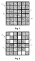
- a matrix addressed display 2 comprises individual pixels. These pixels 4 can take all kinds of shapes, e.g. they can take the forms of characters.
- the examples of matrix displays 2 given in Fig. 1 to Fig. 3 have rectangular or square pixels 4 arranged in rows and columns.
- Fig. 1 illustrates an image of a perfect display 2 having equal luminance response in all pixels 4 when equally driven. Every pixel 4 driven with the same signal renders the same luminance.
- Fig. 2 and Fig. 3 illustrate different cases where the pixels 4 of the displays 2 are also driven by equal signals but where the pixels 4 render a different luminance, as can be seen by the different grey values in the different drawings.
- the spatial distribution of the luminance differences of the pixels 4 can be arbitrary. It is also found that with many technologies, this distribution changes as function of the applied drive to the pixels indicating different response relationships for the pixels 4. For a low drive signal leading to low luminance, the spatial distribution pattern can differ from the pattern at higher driving signal.
- the ligth-output of each individual pixel has to be known, and thus detected.
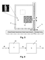
- the present invention provides a vision measurement system, a set-up for automated, electronic vision of the individual pixels of the matrix addressed display, i.e. for measuring the light-output, e.g. luminance; emitted or reflected (depending on the type of display) by individual pixels 4, using a vision measurement set-up.
- the vision measurement system comprises an image capturing device 6, 12 and possibly a movement device 5 for moving the image capturing device 6, 12 and the display 2 with respect to each other. Two embodiments are given as an example, although other electronic vision implementations may be possible reaching the same result: an electronic image of the pixels.
- the matrix addressed display 2 is placed with its light emitting side against an image capturing device, for example is placed face down on a flat bed scanner 6.
- the flat bed scanner 6 may be a suitably modified document or film scanner.
- the spatial resolution of the scanner 6 is so as to allow for adequate vision of the individual pixels 4 of the display 2 under test.
- the sensor 8 and image processing hardware of the flat bed scanner 6 also have enough luminance sensitivity and resolution in order to give a precise quantisation of the luminance emitted by the pixels 4.
- the light source 10 or lamp of the scanner 6 is switched off: the luminance measured is emitted by the display 2 itself.
- the light source 10 or lamp of the scanner 6 is switched on: the light emitted by the display 2 is light from the scanner's light source 10, modulated by the reflective properties of the display 2, and reflected, and is subsequently measured by the sensor 8 of the scanner 6.
- the output file of the image capturing device, in the embodiment described scanner 6, is an electronic image file giving a detailed picture of the pixels 4 of the complete electronic display 2.
- an image capturing device such as e.g. a high resolution CCD camera 12 is used to take a picture of the pixels 4 of the display 2.
- the resolution of the CCD camera 12 is so as to allow adequate definition of the individual pixels 4 of the display 2 to be characterised.
- high resolution electronic displays 2 with an image diagonal of more than 20" require that the CCD camera 12 and the display 2 are moved with respect to each other, e.g.
- the CCD camera 12 is scanned (in X-Y position) over the image surface of the display 2, or vice versa: the display 2 is scanned over the sensor area of the CCD camera 12, in order to take several pictures of different parts of the display area 2.
- the pictures obtained in this way are thereafter preferably stitched to obtain one image of the complete active image surface of the display 2.
- the resulting electronic image file i.e. the output file of the image capturing device, which is in the embodiment described a CCD camera 12, gives a detailed picture of the pixels 1 of the display 2 that needs to be characterised.
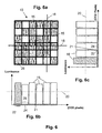
- An example of an image 13 of the pixels 4 of a matrix display 2 is visualised in Fig. 6a.
- the actual location of the matrix display pixels 4 is identified and related to the pixels of the electronic image, for example of the CCD or scanner image.
- a black raster 15 can be distinguished. This characteristic can be used in the algorithms to clearly separate and distinguish the matrix display pixels 4.
- the luminance distribution on an imaginary line in a first direction, e.g. vertical line 16 in a Y-direction, and across an imaginary line in a second direction, e.g. horizontal line 18 in an X-direction, through a pixel 4 can be extracted using imaging software, as illustrated in Fig. 6a to Fig. 6c. Methods of extracting features from images are well known, e.g. as described in "Intelligent Vision Systems for Industry", B. G. Batchelor and P. F.
- the image generated by the matrix display 2 when the image was acquired by the image capturing device 6, 12 was set on all pixels 4 having a first value, e.g. all white pixels 4 or all pixels 4 fully on. Then the luminance distribution across vertical line 16 and horizontal line 18, in the image 13 acquired by the image capturing device 6, 12, shows peaks 19 and valleys 21, that correspond with the actual location of the matrix display pixels 4, as shown in Fig. 6b and Fig. 6c respectively.
- the spatial resolution of the image capturing device e.g. the scanner 6 or the CCD camera 12 needs to be high enough, i.e. higher than the resolution of the matrix display 2, e.g.
- the matrix display 2 preferably at least ten times higher than the resolution of the matrix display 2 (10x over-sampling). Because of the over-sampling, it will be possible to express the horizontal and vertical distance of the matrix display pixels 4 precisely in units of pixels of the image capturing device 6, 12 (not necessarily integer numbers).
- a threshold luminance level 20 is constructed that is located at a suitable value between the maximum luminance level measured at the peaks 19 and minimum luminance level measured at the valleys 21 across the vertical lines 16 and the horizontal lines 18, e.g. approximately in the middle. All pixels of the image capturing device 6, 12 with luminance below the threshold level 20 indicate the location of the black raster 15 in the image, and thus of a corresponding black matrix raster 14 in the display 2. These locations are called in the present description "black matrix locations" 22. The most robust algorithm will consider a pixel location of the image capturing device 6, 12 which is located in the middle between two black matrix locations 22 as the centre of a matrix display pixel 4. Such locations are called “matrix pixel centre locations" 24.
- an amount of image capturing device pixels located around the matrix pixel centre locations 24 across vertical line 16 and horizontal line 18, can be expected to represent the luminance of one matrix display pixel 4.
- these image capturing device pixels e.g. CCD pixels
- CCD pixels are located in the hatched area 26 and are indicated with numbers 1 to 7 in Fig. 6b.
- These CCD pixels are called "matrix pixel locators" 28 in the following.
- the matrix pixel locators 28 are defined for one luminance level of the acquired image 13. To make the influence of noise minimal, the luminance level is preferably maximised (white flat field when acquiring the image).
- a limited number of marker pixels i.e. matrix display pixels 4 with a driving signal which is different from the driving signal of the other matrix pixels 4 of which an electronic image is being taken
- four matrix display pixels 4 ordered in a rectangular shape can be driven with a higher driving level than the other matrix display pixels 4.
- the centre of each marker pixel can then be defined as the centre of the local area with higher luminance.
- interpolation can be used to determine the location of the other matrix display pixels present in the electronic image. This can be done easily since the location of the other matrix display pixels is known relative to the marker pixels a priori (defined by the matrix display pixel structure).
- An advantage of this algorithm compared to the one of the previous embodiment is that a lower degree of over-sampling is necessary since it is not necessary anymore to be able to isolate the black matrix in the electronic image. Therefore, lower resolution image capturing devices 6, 12 can be used.
- the algorithm can also be used for matrix displays where no black matrix structure is present or for matrix displays that also have black matrix between sub-pixels or parts of sub-pixels, such as a colour pixel for example.
- the vision set-up is then slightly different, and comprises a colour measurement device, such as a colorimetric camera or a scanning spectrograph for example.
- a colour measurement device such as a colorimetric camera or a scanning spectrograph for example.
- the underlying principle is the same: a location of a pixel and its colour are determined.
- the luminance of the matrix pixel locators 28 across the X-direction and Y-direction that describe one pixel location, are averaged to one luminance value using a suitable calculation method, e.g. the standard formula for calculation of a mean.
- a suitable calculation method e.g. the standard formula for calculation of a mean.
- every pixel 4 of the matrix display 2 that is to be characterised is assigned a pixel value (a representative or averaged luminance value).
- harmonic mean can be used, or a number of pixel values from the image 13 can be rejected from the mean formula as "outliers or noisy image capturing device pixels".
- a similar method may be applied for assigning a colour value to each individual matrix pixel.
- the light-output values, i.e. luminance values and/or colour values, of the individual pixels 4 can be calculated in any of the described ways or any other way for various test images or light-outputs, i.e. for a plurality of test images in which the pixels are driven by different driving levels. Supposing that, in order to obtain a test image, all pixels are driven with the same information, i.e. with the same drive signal or the same driving level, then the displayed image represents a flat field with light-output of the pixels ranging from 0% to 100% depending on the drive signal.
- a complete image 13 of the matrix display 2 under test can be acquired, and the light-output of each individual pixel 4 can be calculated from the acquired image 13 with any of the described algorithms or any other suitable algorithm. If all response points (video level or luminance level) of a given pixel i are then grouped, then the light-output response function of that given pixel i is obtained.
- the response function may be represented by a number of suitable means for storage and retrieval, e.g. in the form of an analytical function, in the form of a look-up table or in the form of a curve.
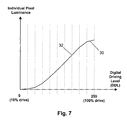
- An example of a luminance response curve 30 is illustrated in Fig. 7.
- the luminance response function can be constructed with as many points as desired or required.
- the curve 30 in the example of Fig. 7 is constructed using eleven characterisation points 32, which result from the display and acquisition of images, and the calculation of luminance levels for a given pixel 4. Interpolation between those characterisation points 32 can then be carried out in order to obtain a light-output response of a pixel 4 corresponding to a driving level which is different from that of any of the characterisation points 32.
- Different interpolation methods exist, and are within the skills of a person skilled in the art.
- a light-output response function is thus available for every individual pixel 4 of the matrix display 2 to be characterised.
- the light-output response functions of individual pixels 4 may all be different or the response functions may be reduced to a smaller number of typical or representative functions, and each pixel may be assigned to one of these typical functions.
- each pixel e.g. composed of a number of colour sub-pixels such as red, green and blue sub-pixels
- this means 9 million functions are obtained, each defined by a set of e.g. sixteen values (light-output in function of drive level).
- a pixel's response function is the result of various physical processes, all of them defining the luminance generation process to a certain extent.
- a few of the processes and parameters that influence an individual pixel's light-output response and can cause the response to be different from pixel to pixel are (non-exhaustive list):
- the light-output response of the individual pixels 4 completely describes that pixel's light-output behaviour as a function of the applied drive signal. This behaviour is individual and may differ from pixel to pixel.
- a next algorithm step defines a drive function, e.g. a drive curve, that ensures that a predefined light-output response (from electrical input signal to light-output of the pixel) can be established.
- the overall light-output response functions can be arbitrary, or may follow a required mathematical law, such as a gamma law, a linear curve or a DICOM (Digital Imaging and Communications in Medicine) curve, the choice being defined by the application or type of images to be rendered (medical images, graphics art images, video editing etc.).
- this next algorithm step provides a correction principle to generate a required light-output response curve for an individual pixel 4, and thus to equalise the response of all pixels 4 in a display 2.
- a display pixel 4 is represented as a black box with an electrical input Pi and an optical output Yi.
- Display pixel 4 has a light-output response function represented by a transfer function L, there being one light-output response function and thus one transfer function L for every individual pixel 4 (e.g. pixels that can be driven independently from other pixels) in the display 2.
- This display pixel 4 is preceded by a transformation circuit 34 that transforms an electrical drive signal Ei into an electrical signal Pi.
- the present invention is not limited to electrical drive signals, e.g. transformation from optical signals to optical signals, or from any other suitable information carrier to any suitable information carrier are also possible.
- the transformation of the drive signal e.g.
- the electrical drive signal Ei into an electrical signal Pi carried out by the transformation circuit 34, may be different for every pixel 4, and is depending on the light-output response function L of that pixel 4.
- the transformation circuit 34 is transforming digital or analog signals, is not relevant to the invention.
- the most straightforward way to realise this transformation circuit 34 is a digital look-up table as will be shown further.
- the counter i in the electrical drive signals Ei, the electrical signal Pi and the light-output signal, e.g. luminance signal Yi
- the transformation circuit has a transfer function T, which may be different for every pixel. Its purpose is to transform the drive signal, e.g electrical signal Ei in such a way to a signal Pi so that a predefined and identical overall light-output, e.g. luminance response Yi versus Ei (further noted as Yi / Ei) is generated for every individual pixel 4, even if the light-output response curves, e.g. luminance response curves Li of these pixels 4 differ.
- luminance correction is explained.
- the luminance response function L of an individual pixel 4 is an S-shaped curve 30 in this example, although other types of characteristic curve can be obtained from the characterization process step as described above depending upon the materials used and the type of display.
- the required overall response for the complete circuit Yi versus Ei is a linear curve 36. Therefore, as can be seen in Fig. 9, the transfer function T has to have particular characteristics, i.e. it may for example be a curve 38 of a particular shape.
- a transfer curve 38 is obtained by mirroring the pixel characteristic curve 30 around a linear curve with slope 1.
- the response function T for a particular pixel 4 complementary to the luminance response L of that particular pixel 4, yields an overall response Yi/Ei which is linear.
- Pixels 4 of the same electronic display 2 may show a different response behaviour, leading to a different characteristic luminance response function L.
- the transfer curves L of the individual pixels 4 can differ to a great extent. Due to the effects described above, pixels 4 can show a basically different response behaviour L.
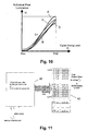
- Some examples of different luminance response curves are shown in Fig. 10 as measured on real displays. Some pixels 40 may exhibit a lower luminance at maximum drive level, as illustrated by curves B and D in Fig. 10. Some other pixels may exhibit higher luminance than other pixels at low drive levels, as illustrated by curve C in Fig. 10.
- each pixel could be made to show a behaviour as indicated by the curve indicated with D.
- the output response Yi of the pixel with curve A would need to be attenuated at PIM, while the output response Yi at Pim would need to be increased.
- it is not necessary to equalise the behaviour of all of the pixels one could choose to not fully equalise certain display pixels because of other (negative) effects.
- not increasing the output response Yi at Pim will result in a higher contrast ratio.
- the screen comprises pixels each having various sub-pixels, e.g. red (R), green (G) and blue (B) sub-pixels.
- the sub-pixels of a colour display may be characterised, and the required colour of the pixel, i.e. luminance of the individual colour sub-pixels, may be calculated such that a uniform colour behaviour of all pixels over the complete screen area is obtained.
- the response curve of each colour element is exactly the same as any other of the same function. Humans experience colour in such a way that spectral differences, if small enough, are not perceived.
- this error figure is small enough then small deviations in the colour output go unnoticed.
- an optimisation of a colour display includes capturing the luminosity and/or colour output of all the pixels and/or pixel elements and optimising the drive characteristics so that all pixels (or a selected number of such pixels - the others being defect pixels) have a luminosity and colour range within the acceptable limits as defined by the above equation.
- a similar technique can also be used to realise a wanted non-uniformity of the screen with respect to its light-output, i.e. colour and/or luminance, behaviour.
- a flat, spatially uniform behaviour of the light-output it can be the object of the matrix display to realise a non-uniform spatial behaviour that corresponds to a target spatial function.
- certain visualisation systems may include post-processing of the image displayed by the matrix display element, e.g. optical post-processing, which introduces spatial non-uniformities. Examples of such systems are for example, but not limited thereto, projection systems and tiled display systems using magnification lenses.
- the techniques of the invention can be used to introduce a non-uniformity of the light-output behaviour to pre-correct for the behaviour of the post-processing system so as to realise a better uniform behaviour of the image that is produced as the result of the combination of said matrix display and said optical post-processing system.
- the present invention includes within its scope that certain pixels are defined as defect pixels, i.e. that certain pixels are deliberately allowed to provide sub-optimal luminosity rather than reduce the brightness of the rest of the display in order to bring the operation of the remaining pixels within the range of the sub-optimal pixels.
- defect pixels may be dealt with in accordance with the co-pending patent application entitled "Method and device for avoiding image misinterpretation due to defective pixels in a matrix display".
- the present invention includes at least two user-defined states: a maximum brightness display in which some of the pixels perform less than optimally but the remaining pixels are all optimised so that each pixel element operates within the same luminance range as other pixel elements having the same function, e.g. all blue pixel elements.
- the present invention provides a method to classify a pixel's light-output response and thus reduce the data required for correction implementations.
- every pixel 4 has its own characteristic light-output response. It is possible to characterise the light-output response function, and hence the required correction function for a pixel 4, into a set of parameters. More specifically, it is an object of the present invention to map the behaviour of a pixel 4, although possibly different for each individual pixel 4, into categories that describe the required correction for a set of pixels. In that sense, various similarly behaving pixels can be categorised as suitable for using the same correction curve. An aim of this technique is to realise a reduction of the required data volume and associated storage memory to realise the correction in hardware circuitry. As an example, a 1 Megapixel display 2 would have for each pixel one characteristic light-output response, which can be stored under the form of e.g. a LUT.
- a first embodiment classifies the actual light-output response functions or curves found into a set of typical curves, based on closest resemblance of the actual curves with the typical curves.
- the type of technique used is not the subject of this invention, but the fact that data reduction techniques are used to come to a typical correction curve may be an aspect of the present invention. The end result is that e.g.
- the correction curves can be fully defined by a limited amount of data e.g. an 8-bits value per pixel, reducing the required hardware (mainly memory) to implement the correction.
- This data set may be called the pixel profile map (PPM).
- PPM pixel profile map
- the 8-bit value may be a pointer to a set of 256 different types of different typical functions.
- These typical functions may e.g. be stored as curves - a set of data points -, as look-up tables or in any other suitable form, such as for example as polynomials or by describing each curve by a vector to its points, in a memory for later use.
- a further embodiment of the present invention does not use classification into typical curves to obtain the PPM.
- the coefficients a, b, ... z will be stored for each pixel in method 2.
- the PCD can for example be approximated by a linear curve defining just an offset (coefficient a) and gain (coefficient b) parameter.
- the coefficients a and b are stored in memory for later use.
- the parameters can be quantified with various resolutions depending on the desired precision. Any combination of typical curves and polynomial description, or any other mathematical description method such as, but not limited to, sin- or cos-series, is also possible.
- the overall result of the pixel characterization and classification is that the PPM is obtained for every pixel 4 of the display device 2 under test.
- the present invention provides a correction circuit to generate a required pixel response curve in real time.
- the correction circuit will apply a specific transfer curve correction for each individual pixel 4, and this synchronous with a pixel clock.
- the transfer curve correction is realized by means of a look-up table.
- the correction circuit provides in a dynamic switching of the look-up table at the frequency of the pixel clock. Associated with every pixel-value is the information about its typical light-output response curve. Thus, at every pixel, it is required to point to the correct look-up table, e.g. that look-up table containing the right correction function for that individual pixel.
- the video memory 40 is 16-bit wide per colour, this means a 48-bit wide digital word to define a colour pixel. It contains for every (sub)pixel the pixel-value itself (8 bit value) and another 8 bit value identifying the pixel's response curve. This latter value is the result of the characterization process of the pixel, followed by the classification process of the pixel's response curve.
- this pixel value is used as a pointer to a bank of different 8 to 8 bit look-up tables 42, actually representing 256 different correction classes available for this display's pixels.
- the principle of look-up tables is well known by persons skilled in the art and allows for a real time implementation at the highest pixel clock speeds as found in today's display controllers.
- a second embodiment can be based on the second classification method that stores the pixel correction curves by means of polynomial descriptors.
- a processing unit will retrieve for every pixel the stored coefficients a, b, c, ..., z and will calculate in real time or off-line the required drive y for the pixel, at a given value x defined by the actual pixel value.
- the correction of the drive value to the pixels can be applied in real time using hardware or software methods, but it can also be carried out off-line (not in real time), e.g. by means of software.
- Software methods may be optimal where cost must be minimized or where dedicated hardware is not available or is to be avoided.
- Such software methods are based upon a microprocessor or similar processing engine such as Programmable Logic Arrays (PLA), Programmable Array Logic (PAL), Gate Arrays especially Field Programmable Gate Arrays (FPGA) for executing the methods described above.
- PPA Programmable Logic Arrays
- PAL Programmable Array Logic
- FPGA Field Programmable Gate Arrays
- processing engines may be embedded in dedicated circuitry such as a VLSI.
- the PPM of the complete display 2 can be made accessible by a software application.
- This application will process every individual pixel with a LUT correction as defined by the PPM data. In that way, the image will be pre-corrected according to the actual display characteristics, before it is generated by the imaging hardware.
Landscapes
- Engineering & Computer Science (AREA)
- Physics & Mathematics (AREA)
- Computer Hardware Design (AREA)
- General Physics & Mathematics (AREA)
- Theoretical Computer Science (AREA)
- Control Of Indicators Other Than Cathode Ray Tubes (AREA)
Priority Applications (1)
| Application Number | Priority Date | Filing Date | Title |
|---|---|---|---|
| EP02447233A EP1424672A1 (fr) | 2002-11-29 | 2002-11-29 | Procédé de commande et dispositif de correction des non-uniformités des pixels d'un dispositif d'affichage à matrice |
Applications Claiming Priority (1)
| Application Number | Priority Date | Filing Date | Title |
|---|---|---|---|
| EP02447233A EP1424672A1 (fr) | 2002-11-29 | 2002-11-29 | Procédé de commande et dispositif de correction des non-uniformités des pixels d'un dispositif d'affichage à matrice |
Publications (1)
| Publication Number | Publication Date |
|---|---|
| EP1424672A1 true EP1424672A1 (fr) | 2004-06-02 |
Family
ID=32241396
Family Applications (1)
| Application Number | Title | Priority Date | Filing Date |
|---|---|---|---|
| EP02447233A Withdrawn EP1424672A1 (fr) | 2002-11-29 | 2002-11-29 | Procédé de commande et dispositif de correction des non-uniformités des pixels d'un dispositif d'affichage à matrice |
Country Status (1)
| Country | Link |
|---|---|
| EP (1) | EP1424672A1 (fr) |
Cited By (15)
| Publication number | Priority date | Publication date | Assignee | Title |
|---|---|---|---|---|
| WO2005101360A1 (fr) * | 2004-03-30 | 2005-10-27 | Eastman Kodak Company | Dispositif a affichage electroluminescent organique |
| EP1650730A1 (fr) | 2004-10-25 | 2006-04-26 | Barco NV | Correction optique pour panneau lumineux d' uniformité élevée |
| EP1806725A2 (fr) * | 2006-01-09 | 2007-07-11 | Samsung Electronics Co., Ltd. | LCD capable de contrôler la luminance de l'écran et procédé de contrôle de la luminance correspondant |
| WO2008057316A2 (fr) * | 2006-11-03 | 2008-05-15 | Eastman Kodak Company | Compensation de l'uniformité d'un écran électroluminescent |
| US7639849B2 (en) | 2005-05-17 | 2009-12-29 | Barco N.V. | Methods, apparatus, and devices for noise reduction |
| EP2239722A2 (fr) | 2009-04-06 | 2010-10-13 | Canon Kabushiki Kaisha | Procédé d'acquisition de valeur de correction, procédé de correction et appareil d'affichage d'images |
| US20110115831A1 (en) * | 2009-11-17 | 2011-05-19 | Samsung Mobile Display Co., Ltd. | Multivision display device and driving method therefor |
| US8164598B2 (en) | 2006-11-19 | 2012-04-24 | Barco N.V. | Display assemblies and computer programs and methods for defect compensation |
| WO2012089848A1 (fr) | 2010-12-31 | 2012-07-05 | Barco N.V. | Dispositif d'affichage et moyen pour améliorer l'uniformité de luminance |
| WO2012089849A1 (fr) | 2010-12-31 | 2012-07-05 | Barco N.V. | Procédé et système pour la compensation d'effets dans des dispositifs d'affichage électroluminescents |
| US8311366B2 (en) | 2006-01-13 | 2012-11-13 | Fraunhofer-Gesellschaft zur Förderung der angewandten Forschung e.V. | System and method for calibrating and adjusting a projected image of a projection apparatus |
| WO2013164015A1 (fr) | 2012-04-30 | 2013-11-07 | Barco N.V. | Système de capteur semi-transparent intégré dans un dispositif d'affichage et son utilisation |
| EP3151227A4 (fr) * | 2014-05-30 | 2017-12-13 | Boe Technology Group Co. Ltd. | Procédé de compensation de luminosité de dispositif d'affichage, appareil de compensation de luminosité et dispositif d'affichage |
| US10043443B2 (en) | 2014-05-30 | 2018-08-07 | Boe Technology Group Co., Ltd. | Display device and method and apparatus for compensating luminance of display device |
| CN113016023A (zh) * | 2018-11-28 | 2021-06-22 | Eizo株式会社 | 信息处理方法以及计算机程序 |
Citations (4)
| Publication number | Priority date | Publication date | Assignee | Title |
|---|---|---|---|---|
| US5359342A (en) * | 1989-06-15 | 1994-10-25 | Matsushita Electric Industrial Co., Ltd. | Video signal compensation apparatus |
| EP1132884A2 (fr) * | 2000-03-10 | 2001-09-12 | Ngk Insulators, Ltd. | Système et procédé d'affichage pour afficher des images fixes et animées |
| US20020075277A1 (en) * | 2000-01-26 | 2002-06-20 | Seiko Epson Corporation | Non-uniformity correction for displayed images |
| US20020154076A1 (en) * | 2000-01-21 | 2002-10-24 | Greene Raymond G. | Construction of large, robust, monolithic and monolithic-like, amlcd displays with wide view angle |
-
2002
- 2002-11-29 EP EP02447233A patent/EP1424672A1/fr not_active Withdrawn
Patent Citations (4)
| Publication number | Priority date | Publication date | Assignee | Title |
|---|---|---|---|---|
| US5359342A (en) * | 1989-06-15 | 1994-10-25 | Matsushita Electric Industrial Co., Ltd. | Video signal compensation apparatus |
| US20020154076A1 (en) * | 2000-01-21 | 2002-10-24 | Greene Raymond G. | Construction of large, robust, monolithic and monolithic-like, amlcd displays with wide view angle |
| US20020075277A1 (en) * | 2000-01-26 | 2002-06-20 | Seiko Epson Corporation | Non-uniformity correction for displayed images |
| EP1132884A2 (fr) * | 2000-03-10 | 2001-09-12 | Ngk Insulators, Ltd. | Système et procédé d'affichage pour afficher des images fixes et animées |
Non-Patent Citations (1)
| Title |
|---|
| "Digital Imaging and Communications in Medicine (DICOM) Part 14: Grayscale Standard Display function", 1998, NATIONAL ELECTRICAL MANUFACTURERS ASSOCIATION, ROSSLYN, VIRGINIA, USA * |
Cited By (31)
| Publication number | Priority date | Publication date | Assignee | Title |
|---|---|---|---|---|
| WO2005101360A1 (fr) * | 2004-03-30 | 2005-10-27 | Eastman Kodak Company | Dispositif a affichage electroluminescent organique |
| US7834825B2 (en) | 2004-03-30 | 2010-11-16 | Global Oled Technology Llc | Organic electroluminescent display apparatus |
| US9384710B2 (en) | 2004-10-25 | 2016-07-05 | Barco N. V. | Optical correction for high uniformity panel lights |
| EP1650730A1 (fr) | 2004-10-25 | 2006-04-26 | Barco NV | Correction optique pour panneau lumineux d' uniformité élevée |
| WO2006045586A1 (fr) * | 2004-10-25 | 2006-05-04 | Barco N.V. | Correction optique pour voyants lumineux de panneau a uniformite elevee |
| US9916795B2 (en) | 2004-10-25 | 2018-03-13 | Barco N.V | Optical correction for high uniformity panel lights |
| JP2008518388A (ja) * | 2004-10-25 | 2008-05-29 | バルコ・ナムローゼ・フエンノートシャップ | 高均一パネルライトの光学補正 |
| US9070316B2 (en) | 2004-10-25 | 2015-06-30 | Barco Nv | Optical correction for high uniformity panel lights |
| USRE43707E1 (en) | 2005-05-17 | 2012-10-02 | Barco N.V. | Methods, apparatus, and devices for noise reduction |
| US7639849B2 (en) | 2005-05-17 | 2009-12-29 | Barco N.V. | Methods, apparatus, and devices for noise reduction |
| EP1806725A3 (fr) * | 2006-01-09 | 2008-08-27 | Samsung Electronics Co., Ltd. | LCD capable de contrôler la luminance de l'écran et procédé de contrôle de la luminance correspondant |
| EP1806725A2 (fr) * | 2006-01-09 | 2007-07-11 | Samsung Electronics Co., Ltd. | LCD capable de contrôler la luminance de l'écran et procédé de contrôle de la luminance correspondant |
| US8311366B2 (en) | 2006-01-13 | 2012-11-13 | Fraunhofer-Gesellschaft zur Förderung der angewandten Forschung e.V. | System and method for calibrating and adjusting a projected image of a projection apparatus |
| US7773062B2 (en) | 2006-11-03 | 2010-08-10 | Global Oled Technology Llc | Method and apparatus for uniformity compensation in an electroluminescent display |
| US7773061B2 (en) | 2006-11-03 | 2010-08-10 | Global Oled Technology Llc | Method and apparatus for uniformity compensation in an OLED display |
| WO2008057316A3 (fr) * | 2006-11-03 | 2008-07-24 | Eastman Kodak Co | Compensation de l'uniformité d'un écran électroluminescent |
| WO2008057316A2 (fr) * | 2006-11-03 | 2008-05-15 | Eastman Kodak Company | Compensation de l'uniformité d'un écran électroluminescent |
| US8164598B2 (en) | 2006-11-19 | 2012-04-24 | Barco N.V. | Display assemblies and computer programs and methods for defect compensation |
| CN101859526A (zh) * | 2009-04-06 | 2010-10-13 | 佳能株式会社 | 校正值获取方法、校正方法和图像显示装置 |
| EP2239722A3 (fr) * | 2009-04-06 | 2011-07-20 | Canon Kabushiki Kaisha | Procédé d'acquisition de valeur de correction, procédé de correction et appareil d'affichage d'images |
| EP2239722A2 (fr) | 2009-04-06 | 2010-10-13 | Canon Kabushiki Kaisha | Procédé d'acquisition de valeur de correction, procédé de correction et appareil d'affichage d'images |
| US20110115831A1 (en) * | 2009-11-17 | 2011-05-19 | Samsung Mobile Display Co., Ltd. | Multivision display device and driving method therefor |
| WO2012089849A1 (fr) | 2010-12-31 | 2012-07-05 | Barco N.V. | Procédé et système pour la compensation d'effets dans des dispositifs d'affichage électroluminescents |
| WO2012089848A1 (fr) | 2010-12-31 | 2012-07-05 | Barco N.V. | Dispositif d'affichage et moyen pour améliorer l'uniformité de luminance |
| WO2013164015A1 (fr) | 2012-04-30 | 2013-11-07 | Barco N.V. | Système de capteur semi-transparent intégré dans un dispositif d'affichage et son utilisation |
| EP3151227A4 (fr) * | 2014-05-30 | 2017-12-13 | Boe Technology Group Co. Ltd. | Procédé de compensation de luminosité de dispositif d'affichage, appareil de compensation de luminosité et dispositif d'affichage |
| US10043443B2 (en) | 2014-05-30 | 2018-08-07 | Boe Technology Group Co., Ltd. | Display device and method and apparatus for compensating luminance of display device |
| US10453384B2 (en) | 2014-05-30 | 2019-10-22 | Boe Technology Group Co., Ltd. | Luminance compensation method of display device, luminance compensation device and display device |
| CN113016023A (zh) * | 2018-11-28 | 2021-06-22 | Eizo株式会社 | 信息处理方法以及计算机程序 |
| CN113016023B (zh) * | 2018-11-28 | 2023-06-27 | Eizo株式会社 | 信息处理方法以及计算机可读的非暂时性记录介质 |
| US11776114B2 (en) | 2018-11-28 | 2023-10-03 | Eizo Corporation | Information processing method and computer program |
Similar Documents
| Publication | Publication Date | Title |
|---|---|---|
| US7639849B2 (en) | Methods, apparatus, and devices for noise reduction | |
| US11170680B2 (en) | Method and apparatus for acquiring Mura compensation data, computer device and storage medium | |
| EP1424672A1 (fr) | Procédé de commande et dispositif de correction des non-uniformités des pixels d'un dispositif d'affichage à matrice | |
| CN108492776B (zh) | 一种amoled屏亮度不均智能外部光学补偿方法 | |
| US6791566B1 (en) | Image display device | |
| US8442316B2 (en) | System and method for improving color and brightness uniformity of backlit LCD displays | |
| US8228348B2 (en) | Method and device for improving spatial and off-axis display standard conformance | |
| KR102590142B1 (ko) | 디스플레이장치 및 그 제어방법 | |
| US20190228737A1 (en) | Screen Calibration Method and Screen Calibration System Capable of Correcting Full Screen Color Tones Automatically | |
| CN110599961B (zh) | 显示面板的灰阶补偿方法、装置及系统 | |
| CN102831870A (zh) | 显示装置和显示装置的亮度不均校正方法 | |
| CN102142224B (zh) | 显示装置、亮度不均补正方法、补正数据制作装置和补正数据制作方法 | |
| JP5174837B2 (ja) | 表示装置、輝度ムラ補正方法、補正データ作成装置、および補正データ作成方法 | |
| US8537144B2 (en) | Method and device for avoiding image misinterpretation due to defective pixels in a matrix display | |
| KR20170047449A (ko) | 표시 장치 및 이의 휘도 보정방법 | |
| JP2011039451A (ja) | 表示装置、輝度ムラ補正方法、補正データ作成装置、および補正データ作成方法 | |
| US7808459B2 (en) | Light emitting display device | |
| KR20050008531A (ko) | 표시장치, 표시장치의 제조방법, 정보처리장치, 보정치의결정방법 및 보정치 결정장치 | |
| CN114387927A (zh) | 显示装置及影像校正方法 | |
| Kim et al. | High-precision color uniformity based on 4D transformation for micro-LED | |
| JP4865849B2 (ja) | 撮像条件決定装置、撮像条件決定方法、撮像条件決定プログラム、コンピュータ読み取り可能な記録媒体、及び上記撮像条件決定装置を備えたムラ補正システム | |
| US8035651B2 (en) | Method of adjusting displaying state of display apparatus | |
| US11810531B1 (en) | Methods and systems for calibrating and controlling a display device | |
| EP1424673A1 (fr) | Méthode et dispositif pour éviter une interprétation d'image fautive par suite de pixels défectueux dans une matrice d'affichage | |
| CN117392930B (zh) | 一种基于CIEXYZ数据进行高效Demura处理的方法和系统 |
Legal Events
| Date | Code | Title | Description |
|---|---|---|---|
| PUAI | Public reference made under article 153(3) epc to a published international application that has entered the european phase |
Free format text: ORIGINAL CODE: 0009012 |
|
| AK | Designated contracting states |
Kind code of ref document: A1 Designated state(s): AT BE BG CH CY CZ DE DK EE ES FI FR GB GR IE IT LI LU MC NL PT SE SK TR |
|
| AX | Request for extension of the european patent |
Extension state: AL LT LV MK RO SI |
|
| 17P | Request for examination filed |
Effective date: 20041129 |
|
| AKX | Designation fees paid |
Designated state(s): AT BE BG CH CY CZ DE DK EE ES FI FR GB GR IE IT LI LU MC NL PT SE SK TR |
|
| 17Q | First examination report despatched |
Effective date: 20050411 |
|
| STAA | Information on the status of an ep patent application or granted ep patent |
Free format text: STATUS: THE APPLICATION IS DEEMED TO BE WITHDRAWN |
|
| 18D | Application deemed to be withdrawn |
Effective date: 20060525 |