EP1424635A1 - Non volatile memory device architecture, for instance a flash kind, having a serial communication interface - Google Patents
Non volatile memory device architecture, for instance a flash kind, having a serial communication interface Download PDFInfo
- Publication number
- EP1424635A1 EP1424635A1 EP02425730A EP02425730A EP1424635A1 EP 1424635 A1 EP1424635 A1 EP 1424635A1 EP 02425730 A EP02425730 A EP 02425730A EP 02425730 A EP02425730 A EP 02425730A EP 1424635 A1 EP1424635 A1 EP 1424635A1
- Authority
- EP
- European Patent Office
- Prior art keywords
- data
- interface
- pad
- address
- pseudo
- Prior art date
- Legal status (The legal status is an assumption and is not a legal conclusion. Google has not performed a legal analysis and makes no representation as to the accuracy of the status listed.)
- Granted
Links
Images




Classifications
-
- G—PHYSICS
- G06—COMPUTING OR CALCULATING; COUNTING
- G06F—ELECTRIC DIGITAL DATA PROCESSING
- G06F13/00—Interconnection of, or transfer of information or other signals between, memories, input/output devices or central processing units
- G06F13/38—Information transfer, e.g. on bus
- G06F13/42—Bus transfer protocol, e.g. handshake; Synchronisation
- G06F13/4204—Bus transfer protocol, e.g. handshake; Synchronisation on a parallel bus
- G06F13/4234—Bus transfer protocol, e.g. handshake; Synchronisation on a parallel bus being a memory bus
-
- G—PHYSICS
- G11—INFORMATION STORAGE
- G11C—STATIC STORES
- G11C16/00—Erasable programmable read-only memories
- G11C16/02—Erasable programmable read-only memories electrically programmable
- G11C16/06—Auxiliary circuits, e.g. for writing into memory
- G11C16/26—Sensing or reading circuits; Data output circuits
-
- G—PHYSICS
- G11—INFORMATION STORAGE
- G11C—STATIC STORES
- G11C7/00—Arrangements for writing information into, or reading information out from, a digital store
- G11C7/10—Input/output [I/O] data interface arrangements, e.g. I/O data control circuits, I/O data buffers
- G11C7/1006—Data managing, e.g. manipulating data before writing or reading out, data bus switches or control circuits therefor
-
- G—PHYSICS
- G11—INFORMATION STORAGE
- G11C—STATIC STORES
- G11C7/00—Arrangements for writing information into, or reading information out from, a digital store
- G11C7/10—Input/output [I/O] data interface arrangements, e.g. I/O data control circuits, I/O data buffers
- G11C7/1015—Read-write modes for single port memories, i.e. having either a random port or a serial port
- G11C7/1045—Read-write mode select circuits
-
- G—PHYSICS
- G11—INFORMATION STORAGE
- G11C—STATIC STORES
- G11C8/00—Arrangements for selecting an address in a digital store
- G11C8/04—Arrangements for selecting an address in a digital store using a sequential addressing device, e.g. shift register, counter
-
- G—PHYSICS
- G11—INFORMATION STORAGE
- G11C—STATIC STORES
- G11C2216/00—Indexing scheme relating to G11C16/00 and subgroups, for features not directly covered by these groups
- G11C2216/12—Reading and writing aspects of erasable programmable read-only memories
- G11C2216/30—Reduction of number of input/output pins by using a serial interface to transmit or receive addresses or data, i.e. serial access memory
Definitions
- the present invention relates to a non volatile memory device architecture, for instance a Flash kind, having a serial communication interface, in particular for applications with SPI serial communication protocols.
- the invention relates to a standard Flash memory integrated in an input/output interface block to receive memory data and/or addresses from and toward the outside of the device, said interface operating according to a SPI serial communication protocol.
- the invention relates to the development of integrated non volatile memories having a SPI (serial Protocol Interface) serial communication interface, but the following description is made with reference to this field of application for convenience of illustration only.
- SPI Serial Protocol Interface
- Flash EEPROM memory device is integrated on semiconductor with a serial communication interface equipped with an input pin INPUT PAD, an output pin OUTPUT PAD, a system clock signal pin CK_PAD and some other control pins, like SELECT_PAD.
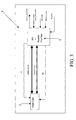
- the block scheme of figure 1 shows the most important memory device blocks and the SPI serial interface.
- the memory device receives through the input pin all protocol codes and all information concerning the addresses, the latter being parallelised by the SPI interface and brought to the flash memory through the address bus ADDR ⁇ 20:0>.
- read data are forced by the Flash Core onto the data bus DBUS ⁇ 15:0> and subsequently serialised and brought outside by means of the output pin.
- the system clock scans the several protocol phases according to the timing sequence shown in figure 2.
- the fall front of the signal applied to the pin SELECT_PAD turns the memory device on and enables all input buffers, the first eight clock beats serve for the instruction code (Read, Write, etc.), the following twenty-four clock beats serve to move to the location address wished to be read or written, they follow therefore the beats required to synchronise the output data on OUTPUT_PAD.
- the output bit number is not previously fixed but it can be set by the user through the SELECT_PAD, the last signal rise front sanctions the end of a reading operation.
- the testing flux software at both EWS (on-wafer-testing) and Final Test (assembled device testing) level has been conceived for a parallel-mode operation.
- They are devices allowing to perform reading/writing operations on flash memories by using a system clock signal scanning the phases of a precise communication protocol at working frequencies of 25 MHz.
- the technical problem underlying the present invention is to provide a non volatile Flash memory architecture equipped with an input/output interface, particularly for SPI serial communication protocol applications, having such structural and functional characteristics as to allow a fast and low-cost testing flux operating yet in the serial mode.
- the solution idea underlying the present invention is to provide a sole input/output interface capable of performing both functions of the serial and parallel type, but with a reduced pin number. Essentially, the parallel operation modes are emulated by the serial interface.
- the semiconductor-integrated non volatile memory device architecture with an input/output interface 2 is globally and schematically indicated with 1.
- Memory device means any monolithical electronic system incorporating a matrix of memory cells 3, organised in rows and columns, as well as circuit portions associated to the cell matrix and in charge of the addressing, decoding, reading, writing and erasing functions of the memory cell content.
- a device of this kind can be for example a semiconductor-integrated memory chip and of the non volatile EEPROM Flash type split in sectors and electrically erasable.
- each memory cell comprises a floating gate transistor having source, drain and control gate terminals.
- a row decoding circuit portion is provided, which is associated to each sector and supplied with specific positive and negative voltages generated internally in the integrated memory circuit by means of positive voltage boosters or charge pumps and regulated by means of corresponding voltage regulators.
- device 1 is equipped also with a pseudo-parallel interface 2 with a low pin number and it exploits some preexistent circuit structures in order to reduce the testing cost of the device itself.
- the pseudo-parallel mode here provided requires at least eleven address pins and eight data pins.
- device 1 is equipped with all the pads necessary for a complete debut at the EWS level, while at the package level only the pads necessary for the SPI serial mode operation will be then connected. Consequently, the package of the semiconductor memory device has only eight pins.
- FIG. 4 shows the timing signal sequence for data reading in this new mode.
- the Clock signal pin serves as synchronism signal; the cell matrix columns are stored on the fall front of this signal and reading is started by means of an ATD (Address Transition Detection) signal.
- ATD Address Transition Detection
- the cell matrix 3 rows are stored on the ATD signal rise front and a new ATD pulse is started.
- the block scheme of figure 3 shows the architecture according to the invention with the mixed SPI serial and pseudo-parallel interface 2, receiving also the signals IC_PAD, the data DATA_PAD ⁇ 7:0> and the addresses ADD_PAD ⁇ 10.0>.
- the signal on the pin IC_PAD allows the one or the other interface to be chosen, i.e. the SPI serial or the parallel, the internal address and data buses will be forced by the one or the other communication phase interface.
- Eight data pins DATA_PAD ⁇ 7:0> are present for the pseudo-parallel mode, one of them being the output pin in the SPI serial mode.
- a first block 4 "State Machine” receives the signals applied on the pins CK_PAD and on the pin SELECT_PAD and it generates the enabling signals (ST ⁇ n:0>) for the various further circuit blocks, according to the particular timing of the protocol used.
- a second block 5 "Instruction Decoder” receives a signal from the less significant pin ADD_PAD ⁇ 0> of the address pin group and it is in charge of decoding in the SPI serial mode the several protocol commands. This block 5 receives the information by the sole input pin ADD_PAD ⁇ 0> of the address pins.
- a third block 6 "Addlatched ⁇ 23:0>" comprises a plurality of latch registers, preferably twenty-four registers, necessary for the temporary storage of the addresses ADD_PAD ⁇ 10:0>.
- a fourth block 7 "Datal ⁇ 7:0>” comprises in turn a group of latch registers, particularly eight registers, and it serves to store temporarily the input and output data on the pins DATA_PAD ⁇ 8:0>.
- a fifth block 8 "Pulse Latching Gen” generates all the enabling signals necessary for the address and data load:
- This fifth block 8 produces a series of signals described below:
- SPI_EN_ADD ⁇ 21:0> are the address bit latching pulses in the SPI mode; each pulse stores a sole address bit.
- SPI_EN_DATA ⁇ 7:0> are the enabling pulses for generating serially the output datum.
- COL_PULSE and ROW_PULSE serves to store the ADD_PAD ⁇ 10:0> content in the block 6 Addlatched as less significant part and as most significant part, respectively. These signals are used only in the pseudo-serial mode.
- DQ_PULSE serves to generate output data in the pseudo-parallel mode.
- Figures 6 and 7 show in greater detail the address and data fluxes being exchanged in blocks 6 and 7 Addlatched and Datal .
- the SPI serial mode will be analysed first.
- the enabling signals of the various address latches are generated on the clock signal rise front, therefore the twenty-four address bits are stored.
- Block 9 Enable Gen is intended to generate both the first and the following latching pulses on the basis of the logic value of signal IC deciding which of the two interfaces is to be used.
- the device according to the invention through the simple addition of a combinatory logic, allows applications on SPI buses to be available and testing phases to be performed in reasonable times reducing as much as possible production and industrialisation costs.
Landscapes
- Engineering & Computer Science (AREA)
- Theoretical Computer Science (AREA)
- Physics & Mathematics (AREA)
- General Engineering & Computer Science (AREA)
- General Physics & Mathematics (AREA)
- Microelectronics & Electronic Packaging (AREA)
- For Increasing The Reliability Of Semiconductor Memories (AREA)
Abstract
Description
Claims (10)
- Non volatile memory device architecture, for example of the Flash type, incorporating a memory cell matrix (3) and an input/output interface (2) for receiving memory data and/or addresses from and to the outside of the device, said interface (2) operating according to a serial communication protocol, characterised in that it comprises in said interface (2) a further pseudo-parallel communication portion having a low pin number and incorporating circuit blocks (4, 5, 8) for selecting the one or the other communication mode against an input-received selection signal.
- Architecture according to claim 1, characterised in that said circuit blocks comprise at least a state machine (4) receiving a clock signal and a selection signal for activating the remaining blocks; an instruction decoder block (5) for decoding in the SPI serial mode the various communication protocol commands and an enabling signal generator block (8) for loading data and address registers (6, 7).
- Architecture according to claim 2, characterised in that said interface (2) comprises also a latch register block (6) to store temporarily input and output addresses on address pins (ADD_PAD<10:0>.
- Architecture according to claim 1, characterised in that said interface (2) comprises also a latch register block (7) to store temporarily input and output data on data pins (DATA_PAD<8:0>).
- Architecture according to claim 3, characterised in that said address latch registers are at least twenty-four.
- Architecture according to claim 4, characterised in that said data latch registers are at least eight.
- Architecture according to claim 3, characterised in that said address register block (6) is associated to an enabling pulse generator block (9) to generate latching pulses based on the logic value of a signal (IC) received by said signal generator block (8) and it selects which one of the two serial or pseudo-parallel interface is to be used.
- Architecture according to claim 4, characterised in that said data register block (7) is associated to an enabling pulse generator block (9) to generate latching pulses based on the logic value of a signal (IC) received by said signal generator block (8) and it selects which one of the two serial or pseudo-parallel interface is to be used.
- Architecture according to claim 1, characterised in that said signal generator block (8) produces at least the following signals: SPI_EN_ADD<21:0> for enabling an address bit latching in the SPI serial mode; each pulse stores a sole address bit; SPI_EN_DATA<7:0> for enabling the serial generation of the output datum; COL_PULSE to store in the pseudo-parallel mode the content of the addresses (ADD_PAD<10:0>) in a register block (6) as the less significant part; ROW_PULSE to store the content of the addresses (ADD_PAD<10:0>) in a register block (6) as the most significant part; DQ_PULSE to generate output data still in the pseudo-parallel mode.
- Architecture according to claim 1, characterised in that it comprises eleven address pins (ADD_PAD<10:0>) for the address flow in the pseudo-parallel mode, one of them being used as input pin in the serial mode, as well as eight data pins (DATA_PAD<7:0>) for the pseudo-parallel mode, one of them being used as the output pin in the SPI serial mode.
Priority Applications (3)
| Application Number | Priority Date | Filing Date | Title |
|---|---|---|---|
| DE60229649T DE60229649D1 (en) | 2002-11-28 | 2002-11-28 | Non-volatile memory array architecture, for example of the flash type with a serial transmission interface |
| EP02425730A EP1424635B1 (en) | 2002-11-28 | 2002-11-28 | Non volatile memory device architecture, for instance a flash kind, having a serial communication interface |
| US10/727,341 US7151705B2 (en) | 2002-11-28 | 2003-11-26 | Non-volatile memory device architecture, for instance a flash kind, having a serial communication interface |
Applications Claiming Priority (1)
| Application Number | Priority Date | Filing Date | Title |
|---|---|---|---|
| EP02425730A EP1424635B1 (en) | 2002-11-28 | 2002-11-28 | Non volatile memory device architecture, for instance a flash kind, having a serial communication interface |
Publications (2)
| Publication Number | Publication Date |
|---|---|
| EP1424635A1 true EP1424635A1 (en) | 2004-06-02 |
| EP1424635B1 EP1424635B1 (en) | 2008-10-29 |
Family
ID=32241384
Family Applications (1)
| Application Number | Title | Priority Date | Filing Date |
|---|---|---|---|
| EP02425730A Expired - Lifetime EP1424635B1 (en) | 2002-11-28 | 2002-11-28 | Non volatile memory device architecture, for instance a flash kind, having a serial communication interface |
Country Status (3)
| Country | Link |
|---|---|
| US (1) | US7151705B2 (en) |
| EP (1) | EP1424635B1 (en) |
| DE (1) | DE60229649D1 (en) |
Cited By (7)
| Publication number | Priority date | Publication date | Assignee | Title |
|---|---|---|---|---|
| EP1932158A4 (en) * | 2005-09-30 | 2008-10-15 | Mosaid Technologies Inc | Memory with output control |
| WO2008134481A1 (en) * | 2007-04-25 | 2008-11-06 | Micron Technology Inc. | Nand interface |
| US7558900B2 (en) * | 2004-09-27 | 2009-07-07 | Winbound Electronics Corporation | Serial flash semiconductor memory |
| US8266360B2 (en) | 2007-08-15 | 2012-09-11 | Nxp B.V. | I2C-bus interface with parallel operational mode |
| US9053066B2 (en) * | 2012-03-30 | 2015-06-09 | Sandisk Technologies Inc. | NAND flash memory interface |
| WO2015084534A1 (en) * | 2013-12-02 | 2015-06-11 | Silicon Storage Technology, Inc. | Three-dimensional flash nor memory system with configurable pins |
| US9230654B2 (en) | 2005-09-30 | 2016-01-05 | Conversant Intellectual Property Management Inc. | Method and system for accessing a flash memory device |
Families Citing this family (42)
| Publication number | Priority date | Publication date | Assignee | Title |
|---|---|---|---|---|
| ITVA20030022A1 (en) * | 2003-07-07 | 2005-01-08 | St Microelectronics Srl | METHOD OF GENERATION OF A SIGNAL OF ENABLING IN A MULTI-PROTOCOL MEMORY AND RELATIVE MEMORY DEVICE. |
| US11948629B2 (en) | 2005-09-30 | 2024-04-02 | Mosaid Technologies Incorporated | Non-volatile memory device with concurrent bank operations |
| US20070076502A1 (en) * | 2005-09-30 | 2007-04-05 | Pyeon Hong B | Daisy chain cascading devices |
| US7747833B2 (en) | 2005-09-30 | 2010-06-29 | Mosaid Technologies Incorporated | Independent link and bank selection |
| US8069328B2 (en) * | 2006-03-28 | 2011-11-29 | Mosaid Technologies Incorporated | Daisy chain cascade configuration recognition technique |
| US8335868B2 (en) | 2006-03-28 | 2012-12-18 | Mosaid Technologies Incorporated | Apparatus and method for establishing device identifiers for serially interconnected devices |
| US8364861B2 (en) * | 2006-03-28 | 2013-01-29 | Mosaid Technologies Incorporated | Asynchronous ID generation |
| US7551492B2 (en) | 2006-03-29 | 2009-06-23 | Mosaid Technologies, Inc. | Non-volatile semiconductor memory with page erase |
| KR101194965B1 (en) | 2006-03-31 | 2012-10-25 | 모사이드 테크놀로지스 인코퍼레이티드 | Flash memory system control method |
| CN101174253A (en) * | 2006-06-02 | 2008-05-07 | 旺宏电子股份有限公司 | Method and device for transmitting data on multiple pins of multi-mode bus |
| EP2487794A3 (en) | 2006-08-22 | 2013-02-13 | Mosaid Technologies Incorporated | Modular command structure for memory and memory system |
| US8700818B2 (en) * | 2006-09-29 | 2014-04-15 | Mosaid Technologies Incorporated | Packet based ID generation for serially interconnected devices |
| US7817470B2 (en) | 2006-11-27 | 2010-10-19 | Mosaid Technologies Incorporated | Non-volatile memory serial core architecture |
| US8331361B2 (en) | 2006-12-06 | 2012-12-11 | Mosaid Technologies Incorporated | Apparatus and method for producing device identifiers for serially interconnected devices of mixed type |
| US7853727B2 (en) | 2006-12-06 | 2010-12-14 | Mosaid Technologies Incorporated | Apparatus and method for producing identifiers regardless of mixed device type in a serial interconnection |
| US8271758B2 (en) | 2006-12-06 | 2012-09-18 | Mosaid Technologies Incorporated | Apparatus and method for producing IDS for interconnected devices of mixed type |
| US8010709B2 (en) * | 2006-12-06 | 2011-08-30 | Mosaid Technologies Incorporated | Apparatus and method for producing device identifiers for serially interconnected devices of mixed type |
| US7818464B2 (en) * | 2006-12-06 | 2010-10-19 | Mosaid Technologies Incorporated | Apparatus and method for capturing serial input data |
| US7529149B2 (en) * | 2006-12-12 | 2009-05-05 | Mosaid Technologies Incorporated | Memory system and method with serial and parallel modes |
| US8984249B2 (en) * | 2006-12-20 | 2015-03-17 | Novachips Canada Inc. | ID generation apparatus and method for serially interconnected devices |
| US7613049B2 (en) * | 2007-01-08 | 2009-11-03 | Macronix International Co., Ltd | Method and system for a serial peripheral interface |
| US8010710B2 (en) | 2007-02-13 | 2011-08-30 | Mosaid Technologies Incorporated | Apparatus and method for identifying device type of serially interconnected devices |
| KR101494065B1 (en) * | 2007-02-16 | 2015-02-23 | 컨버전트 인텔렉츄얼 프로퍼티 매니지먼트 인코포레이티드 | Semiconductor device and method for reducing power consumption in a system having interconnected devices |
| US8046527B2 (en) | 2007-02-22 | 2011-10-25 | Mosaid Technologies Incorporated | Apparatus and method for using a page buffer of a memory device as a temporary cache |
| US8086785B2 (en) | 2007-02-22 | 2011-12-27 | Mosaid Technologies Incorporated | System and method of page buffer operation for memory devices |
| US7796462B2 (en) | 2007-02-22 | 2010-09-14 | Mosaid Technologies Incorporated | Data flow control in multiple independent port |
| WO2009062280A1 (en) * | 2007-11-15 | 2009-05-22 | Mosaid Technologies Incorporated | Methods and systems for failure isolation and data recovery in a configuration of series-connected semiconductor devices |
| US7913128B2 (en) | 2007-11-23 | 2011-03-22 | Mosaid Technologies Incorporated | Data channel test apparatus and method thereof |
| US7983099B2 (en) | 2007-12-20 | 2011-07-19 | Mosaid Technologies Incorporated | Dual function compatible non-volatile memory device |
| US7940572B2 (en) | 2008-01-07 | 2011-05-10 | Mosaid Technologies Incorporated | NAND flash memory having multiple cell substrates |
| US7957173B2 (en) * | 2008-10-14 | 2011-06-07 | Mosaid Technologies Incorporated | Composite memory having a bridging device for connecting discrete memory devices to a system |
| US8134852B2 (en) | 2008-10-14 | 2012-03-13 | Mosaid Technologies Incorporated | Bridge device architecture for connecting discrete memory devices to a system |
| US8549209B2 (en) * | 2008-11-04 | 2013-10-01 | Mosaid Technologies Incorporated | Bridging device having a configurable virtual page size |
| US20100115172A1 (en) * | 2008-11-04 | 2010-05-06 | Mosaid Technologies Incorporated | Bridge device having a virtual page buffer |
| GB2513551B (en) | 2010-09-24 | 2018-01-10 | Ibm | High-speed memory system |
| US9697872B2 (en) * | 2011-12-07 | 2017-07-04 | Cypress Semiconductor Corporation | High speed serial peripheral interface memory subsystem |
| TWI501240B (en) * | 2012-06-14 | 2015-09-21 | Winbond Electronics Corp | Flash memory and method for operating memory device |
| US9385721B1 (en) | 2015-01-14 | 2016-07-05 | Sandisk Technologies Llc | Bulk driven low swing driver |
| JP2018014050A (en) * | 2016-07-22 | 2018-01-25 | 東芝メモリ株式会社 | Memory system |
| US9792994B1 (en) | 2016-09-28 | 2017-10-17 | Sandisk Technologies Llc | Bulk modulation scheme to reduce I/O pin capacitance |
| CN111813705B (en) * | 2020-06-28 | 2024-06-14 | 上海华虹宏力半导体制造有限公司 | Serial flash memory and address control method thereof |
| KR20220098947A (en) * | 2021-01-05 | 2022-07-12 | 삼성전자주식회사 | Semiconductor device and electronic device including the same |
Citations (3)
| Publication number | Priority date | Publication date | Assignee | Title |
|---|---|---|---|---|
| US5808929A (en) * | 1995-12-06 | 1998-09-15 | Sheikholeslami; Ali | Nonvolatile content addressable memory |
| US5966723A (en) * | 1997-05-16 | 1999-10-12 | Intel Corporation | Serial programming mode for non-volatile memory |
| US6466505B1 (en) * | 2001-05-02 | 2002-10-15 | Cypress Semiconductor Corp. | Flexible input structure for an embedded memory |
Family Cites Families (3)
| Publication number | Priority date | Publication date | Assignee | Title |
|---|---|---|---|---|
| US4897818A (en) * | 1983-12-30 | 1990-01-30 | Texas Instruments Incorporated | Dual-port memory with inhibited random access during transfer cycles |
| US6510487B1 (en) * | 1996-01-24 | 2003-01-21 | Cypress Semiconductor Corp. | Design architecture for a parallel and serial programming interface |
| US6650141B2 (en) * | 2001-12-14 | 2003-11-18 | Lattice Semiconductor Corporation | High speed interface for a programmable interconnect circuit |
-
2002
- 2002-11-28 EP EP02425730A patent/EP1424635B1/en not_active Expired - Lifetime
- 2002-11-28 DE DE60229649T patent/DE60229649D1/en not_active Expired - Lifetime
-
2003
- 2003-11-26 US US10/727,341 patent/US7151705B2/en not_active Expired - Lifetime
Patent Citations (3)
| Publication number | Priority date | Publication date | Assignee | Title |
|---|---|---|---|---|
| US5808929A (en) * | 1995-12-06 | 1998-09-15 | Sheikholeslami; Ali | Nonvolatile content addressable memory |
| US5966723A (en) * | 1997-05-16 | 1999-10-12 | Intel Corporation | Serial programming mode for non-volatile memory |
| US6466505B1 (en) * | 2001-05-02 | 2002-10-15 | Cypress Semiconductor Corp. | Flexible input structure for an embedded memory |
Cited By (14)
| Publication number | Priority date | Publication date | Assignee | Title |
|---|---|---|---|---|
| US7558900B2 (en) * | 2004-09-27 | 2009-07-07 | Winbound Electronics Corporation | Serial flash semiconductor memory |
| US8427897B2 (en) | 2005-09-30 | 2013-04-23 | Mosaid Technologies Incorporated | Memory with output control |
| US7826294B2 (en) | 2005-09-30 | 2010-11-02 | Mosaid Technologies Incorporated | Memory with output control |
| EP1932158A4 (en) * | 2005-09-30 | 2008-10-15 | Mosaid Technologies Inc | Memory with output control |
| US8654601B2 (en) | 2005-09-30 | 2014-02-18 | Mosaid Technologies Incorporated | Memory with output control |
| US9230654B2 (en) | 2005-09-30 | 2016-01-05 | Conversant Intellectual Property Management Inc. | Method and system for accessing a flash memory device |
| WO2008134481A1 (en) * | 2007-04-25 | 2008-11-06 | Micron Technology Inc. | Nand interface |
| US7916557B2 (en) | 2007-04-25 | 2011-03-29 | Micron Technology, Inc. | NAND interface |
| US8953396B2 (en) | 2007-04-25 | 2015-02-10 | Micron Technology, Inc. | NAND interface |
| US8266360B2 (en) | 2007-08-15 | 2012-09-11 | Nxp B.V. | I2C-bus interface with parallel operational mode |
| US9053066B2 (en) * | 2012-03-30 | 2015-06-09 | Sandisk Technologies Inc. | NAND flash memory interface |
| WO2015084534A1 (en) * | 2013-12-02 | 2015-06-11 | Silicon Storage Technology, Inc. | Three-dimensional flash nor memory system with configurable pins |
| CN105793928A (en) * | 2013-12-02 | 2016-07-20 | 硅存储技术公司 | Three-dimensional flash nor memory system with configurable pins |
| US10373686B2 (en) | 2013-12-02 | 2019-08-06 | Silicon Storage Technology, Inc. | Three-dimensional flash NOR memory system with configurable pins |
Also Published As
| Publication number | Publication date |
|---|---|
| EP1424635B1 (en) | 2008-10-29 |
| DE60229649D1 (en) | 2008-12-11 |
| US7151705B2 (en) | 2006-12-19 |
| US20050213421A1 (en) | 2005-09-29 |
Similar Documents
| Publication | Publication Date | Title |
|---|---|---|
| EP1424635B1 (en) | Non volatile memory device architecture, for instance a flash kind, having a serial communication interface | |
| KR100990541B1 (en) | How to read and write pipeline memory | |
| US5982664A (en) | Semiconductor memory capable of writing and reading data | |
| KR0172366B1 (en) | Read and program method of nonvolatile semiconductor memory device and circuit thereof | |
| US7290109B2 (en) | Memory system and memory card | |
| US7334080B2 (en) | Nonvolatile memory with independent access capability to associated buffer | |
| US6903971B2 (en) | Non-volatile semiconductor memory device | |
| EP1152339A2 (en) | Semiconductor memory device and restoration method therefor | |
| US20120155173A1 (en) | Universal Timing Waveforms Sets to Improve Random Access Read and Write Speed of Memories | |
| WO2003025939A3 (en) | Dynamic column block selection | |
| CN101388239B (en) | Semiconductor memory device | |
| US20110302470A1 (en) | Test mode for parallel load of address dependent data to enable loading of desired data backgrounds | |
| US20050135145A1 (en) | Synchronous flash memory device and method of operating the same | |
| US20030174543A1 (en) | Asynchronous semiconductor memory device | |
| US8423701B2 (en) | Flash memory device with a low pin count (LPC) communication interface | |
| US20020073272A1 (en) | Method of programming a multi-flash memory system | |
| JP2009099202A (en) | Semiconductor memory device | |
| KR100269319B1 (en) | Semiconductor memory device including simultaneous enabling circuit for column select line and control method | |
| JPH03157900A (en) | Error correcting circuit for eeprom | |
| US20120163086A1 (en) | Concurrent operation of plural flash memories | |
| US6785174B2 (en) | Testing method and device for non-volatile memories having a LPC (low pin count) communication serial interface | |
| KR20070033667A (en) | Page buffer of flash memory device and program method using it | |
| US6975559B2 (en) | Device and method for reading non-volatile memories having at least one pseudo-parallel communication interface | |
| EP1435624B1 (en) | Fast page programming architecture and method in a non-volatile memory device with an SPI interface | |
| JPH07192483A (en) | EEPROM, EEPROM write control method, and IC card |
Legal Events
| Date | Code | Title | Description |
|---|---|---|---|
| PUAI | Public reference made under article 153(3) epc to a published international application that has entered the european phase |
Free format text: ORIGINAL CODE: 0009012 |
|
| AK | Designated contracting states |
Kind code of ref document: A1 Designated state(s): AT BE BG CH CY CZ DE DK EE ES FI FR GB GR IE IT LI LU MC NL PT SE SK TR |
|
| AX | Request for extension of the european patent |
Extension state: AL LT LV MK RO SI |
|
| 17P | Request for examination filed |
Effective date: 20041130 |
|
| AKX | Designation fees paid |
Designated state(s): DE FR GB IT |
|
| 17Q | First examination report despatched |
Effective date: 20070725 |
|
| GRAP | Despatch of communication of intention to grant a patent |
Free format text: ORIGINAL CODE: EPIDOSNIGR1 |
|
| GRAS | Grant fee paid |
Free format text: ORIGINAL CODE: EPIDOSNIGR3 |
|
| GRAA | (expected) grant |
Free format text: ORIGINAL CODE: 0009210 |
|
| AK | Designated contracting states |
Kind code of ref document: B1 Designated state(s): DE FR GB IT |
|
| REG | Reference to a national code |
Ref country code: GB Ref legal event code: FG4D |
|
| REF | Corresponds to: |
Ref document number: 60229649 Country of ref document: DE Date of ref document: 20081211 Kind code of ref document: P |
|
| PG25 | Lapsed in a contracting state [announced via postgrant information from national office to epo] |
Ref country code: IT Free format text: LAPSE BECAUSE OF FAILURE TO SUBMIT A TRANSLATION OF THE DESCRIPTION OR TO PAY THE FEE WITHIN THE PRESCRIBED TIME-LIMIT Effective date: 20081029 |
|
| PGFP | Annual fee paid to national office [announced via postgrant information from national office to epo] |
Ref country code: FR Payment date: 20090515 Year of fee payment: 7 |
|
| PLBE | No opposition filed within time limit |
Free format text: ORIGINAL CODE: 0009261 |
|
| STAA | Information on the status of an ep patent application or granted ep patent |
Free format text: STATUS: NO OPPOSITION FILED WITHIN TIME LIMIT |
|
| 26N | No opposition filed |
Effective date: 20090730 |
|
| PGFP | Annual fee paid to national office [announced via postgrant information from national office to epo] |
Ref country code: GB Payment date: 20090518 Year of fee payment: 7 |
|
| GBPC | Gb: european patent ceased through non-payment of renewal fee |
Effective date: 20091128 |
|
| PG25 | Lapsed in a contracting state [announced via postgrant information from national office to epo] |
Ref country code: GB Free format text: LAPSE BECAUSE OF NON-PAYMENT OF DUE FEES Effective date: 20091128 |
|
| REG | Reference to a national code |
Ref country code: FR Ref legal event code: ST Effective date: 20110902 |
|
| PG25 | Lapsed in a contracting state [announced via postgrant information from national office to epo] |
Ref country code: FR Free format text: LAPSE BECAUSE OF NON-PAYMENT OF DUE FEES Effective date: 20091130 |
|
| REG | Reference to a national code |
Ref country code: DE Ref legal event code: R082 Ref document number: 60229649 Country of ref document: DE Representative=s name: SAMSON & PARTNER, PATENTANWAELTE, DE |
|
| REG | Reference to a national code |
Ref country code: DE Ref legal event code: R082 Ref document number: 60229649 Country of ref document: DE Representative=s name: SAMSON & PARTNER, PATENTANWAELTE, DE Effective date: 20130515 Ref country code: DE Ref legal event code: R081 Ref document number: 60229649 Country of ref document: DE Owner name: MICRON TECHNOLOGY, INC., US Free format text: FORMER OWNER: STMICROELECTRONICS S.R.L., AGRATE BRIANZA, IT Effective date: 20130515 Ref country code: DE Ref legal event code: R081 Ref document number: 60229649 Country of ref document: DE Owner name: MICRON TECHNOLOGY, INC., BOISE, US Free format text: FORMER OWNER: STMICROELECTRONICS S.R.L., AGRATE BRIANZA, MAILAND/MILANO, IT Effective date: 20130515 Ref country code: DE Ref legal event code: R082 Ref document number: 60229649 Country of ref document: DE Representative=s name: SAMSON & PARTNER PATENTANWAELTE MBB, DE Effective date: 20130515 Ref country code: DE Ref legal event code: R081 Ref document number: 60229649 Country of ref document: DE Owner name: MICRON TECHNOLOGY, INC., BOISE, US Free format text: FORMER OWNER: STMICROELECTRONICS S.R.L., AGRATE BRIANZA, IT Effective date: 20130515 |
|
| PGFP | Annual fee paid to national office [announced via postgrant information from national office to epo] |
Ref country code: DE Payment date: 20220127 Year of fee payment: 20 |
|
| REG | Reference to a national code |
Ref country code: DE Ref legal event code: R071 Ref document number: 60229649 Country of ref document: DE |