Technical Field
The present invention relates to a method of driving
a liquid crystal display element and a liquid crystal
display device using the method and, particularly, to the
liquid crystal display device employing a liquid crystal
mode capable of achieving a high speed response and a wide
angle of visibility.
Background Art
An active matrix type liquid crystal display using a
thin film transistor (TFT) is used in various fields such
as a display of a camcorder and a display of a personal
computer or a personal word processor owing to its
advantages such as a reduced thickness, a reduced weight,
and capability of low voltage driving, and there is a
large market for such liquid crystal display.
In recent years, particularly, the liquid crystal
display has been used for displaying dynamic images and
has been applied to televisions in addition to the
conventional use for displaying static images in a
personal computer and the like, and there is an increasing
demand for a liquid crystal display device suitable for
such dynamic image display. In order to meet such demand,
a liquid crystal display element of a bend orientation is
proposed in Japanese Unexamined Patent Publication No. 7-84254
as the liquid crystal element which enables
improvements in high speed response required for the
dynamic image display. In the liquid crystal element of
bend orientation, liquid crystals rapidly change with a
change of voltage, thereby realizing the high speed
response. It is possible to achieve such bend orientation
by transitioning an initial orientation which is called
splay orientation through an application of a voltage;
however, the bend orientation undesirably returns to the
splay orientation when the voltage applied to the liquid
crystals is below a predetermined value. In view of the
above problem, the present applicant has filed a Japanese
patent application (Japanese Patent Application No. 2000-214827
which has not been published yet) which proposes a
driving method of a liquid crystal display element,
wherein a signal voltage different from a picture signal
voltage is applied to liquid crystals in order to prevent
the reverse transition from the bend orientation to the
splay orientation.
Also, Japanese Unexamined Patent Publication No. 11-109921
proposes a driving method of a liquid crystal
display element, wherein a blanking image is displayed
using a non-image signal which is inserted between picture
signals so as to reduce a blurring of dynamic image which
is peculiar to the liquid crystals.
This conventional liquid crystal display element
driving method will be explained with reference to the
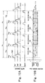
accompanying drawings. Shown in Fig. 12 is a timing chart
indicating contents of gate signals and a source signal in
the conventional liquid crystal display element driving
method, wherein Fig. 12A is a graph showing the gate
signals and Fig. 12B is a graph showing the source signal.
In Figs. 12A and 12B, a gate ON voltage Vgon is
applied to gate lines sequentially using gate signals Sg1
to Sgend, thereby bringing switching elements provided for
respective pixels to an ON state. Then, a source signal
Ssn is supplied from each of source lines to each of the
pixels in accordance with the switching ON timing, and a
potential difference between a pixel electrode and a
counter electrode reaches a value responsive to a voltage
applied by the source signal Ssn. Hereinafter, a state in
which a potential difference between a pixel electrode and
a counter electrode in a certain pixel becomes a
predetermined voltage by the source signal Ssn is
expressed as the source signal is written to the pixel.
In this case, the gate ON voltage Vgon is applied twice to
each of the gate lines during each of frame periods Po and
Pe; a picture signal 101 from the source line is written
as the source signal Ssn to each of the pixels in the
first Vgon application, and a non-picture signal 102 from
the source line is written as the source signal Ssn to
each of the pixels in the second Vgon application. Owing
to the writing of non-picture signal 102, the reverse
transition of liquid crystals to the splay orientation is
prevented in each of the pixel.
By the way, in general liquid crystal display
devices, a liquid crystal display element is AC driven for
the purpose of suppressing burn-in of liquid crystals and
generation of display unevenness due to ions. Accordingly,
the non-picture signal 102 is written to the pixels when
applying the second gate ON voltage Vgon during the odd
frame period Po, and then the picture signal 101 having a
reverse polarity is written to the pixels when applying
the first gate ON voltage Vgon during the succeeding even
frame period Pe. Therefore, the writing of the picture
signal 101 causes a great potential difference, and the
potential of the pixel electrode does not reach the
potential responsive to the picture signal 101 to lead to
generation of the display unevenness.
Further, along with future developments in high
resolution liquid crystal panels, time allowed for writing
one source signal will become shorter and shorter, and,
therefore, it will be necessary to write a signal with
reliability in such shortened period of time.
Disclosure of the Invention
The present invention has been accomplished in view
of the above problems, and a first object thereof is to
provide a liquid crystal display element driving method
and a liquid crystal display device using the method which
enable a picture signal to be rapidly written to a pixel
in the case where a plurality of times of signal writings
are performed for each of the pixels during each of frame
periods as in a liquid crystal display of a bend
orientation.
A second object of the invention is to provide a
liquid crystal display element driving method and a liquid
crystal display device using the method which enable a
picture signal to be written to a pixel with reliability
in the case of high resolution display.
In order to attain the above objects, a liquid
crystal display element driving method or a liquid crystal
display device using the method according to the invention
uses a liquid crystal display element having a plurality
of pixels constituting a screen and comprises a gate
driving step or gate driving means of dividing a frame
period into a plurality of write periods and outputting
gate signals to select the pixels sequentially during the
write periods and a source driving step or source driving
means of forming each of source signals such that the
source signal includes a picture signal and a non-picture
signal assigned for the write periods and writing each of
the source signals corresponding to the selected pixels to
each of the pixels with its polarity being alternated,
thereby controlling a transmittivity of liquid crystals of
each of the pixels in accordance with the written source
signal to display an image responsive to the source
signals on the screen of the liquid crystal display
element, wherein the source driving step or the source
driving means enables to write the non-picture signal to
the pixel with its polarity being identical to that of the
picture signal to be written subsequently.
With such constitution, a potential difference in
the case of writing the picture signal subsequently to the
non-picture signal is reduced, thereby enabling the
picture signal to be rapidly written to the pixel.
In this case, the non-picture signal may be written
to the pixel at least during a last one of the plurality
of write periods in the source driving step or by the
source driving means.
Alternatively, the non-picture signal may be written
to the pixel at least during a first one of the plurality
of write periods in the source driving step or by the
source driving means.
Further, the picture signal and the non-picture
signal may have the same polarity during the frame period.
With such constitution, an amplitude between the
picture signal and the non-picture signal is reduced
during the frame period, thereby reducing time required
for a potential of the source signal to reach a desired
signal potential of each of the pixels and suppressing
influences of resistance in the source line and signal
delay due to parasitic capacitance. Therefore, it is
possible to write the picture signal to the pixel more
rapidly. Further, it is possible to reduce a load on the
source driving means for supplying the source signal.
Also, the pixels may be selected during a plurality
of periods in at least one of the plurality of write
periods in the gate driving step or by the gate driving
means, and the non-picture signal may be written to the
selected pixels during the plurality of periods in the
gate driving step or by the gate driving means.
With such constitution, time allowed for writing the
picture signal to each of the pixels is substantially
increased, thereby enabling the picture signal to be
written to each of the pixels with reliability.
In this case, the plurality of periods may be
consecutive.
With such constitution, rising and falling periods
of the picture signal are reduced, so that the substantial
signal writing time is further increased. Therefore, the
picture signal is written to each of the pixels with
higher reliability.
A liquid crystal display element driving method and
the liquid crystal display device using the method
according to the invention uses a liquid crystal display
element having a plurality of pixels constituting a screen
and comprises a gate driving step or gate driving means
for dividing a frame period into four or more write
periods and outputting gate signals to select the pixels
sequentially during the write periods and a source driving
step or source driving means for forming each of source
signals such that the source signal includes picture
signals corresponding to three colors of red, green, and
blue assigned respectively for three write periods of the
four or more write periods and writing each of the source
signals corresponding to the selected pixels to each of
the pixels with its polarity being alternated, thereby
controlling a transmittivity of liquid crystals of each of
the pixels in accordance with the written source signal to
display a color image responsive to the source signals on
the screen of the liquid crystal display element.
With such constitution, by writing a signal having a
predetermined voltage in a write period other than the
write periods in which the picture signals corresponding
to the three colors of red, green, and blue are written,
it is possible to prevent a reverse transition to a splay
orientation in the liquid crystal display element or the
liquid crystal display device capable of color display.
In this case, in the source driving step or by the
source driving means, each of the source signals may be
formed such that the source signal includes at least one
non-picture signal assigned for the write period other
than the write periods in which the picture signals
corresponding to the three colors of red, green, and blue
are written.
With such constitution, it is possible to prevent
the reverse transition to splay orientation more
effectively.
In this case, in the source driving step or by the
source driving means, the non-picture signal may be
written to the pixels during at least a last one of the
four or more write periods.
Alternatively, in the source driving step or the
source driving means, the non-picture signal may be
written to the pixels during at least a first one of the
four or more write periods.
Also, in the source driving step or by the source
driving means, the picture signals may be written to the
pixels with their polarities being alternated.
With such constitution, the liquid crystals are AC
driven with a higher frequency thereby to further suppress
display unevenness.
A liquid crystal display element driving method and
the liquid crystal display device using the method
according to the invention uses a liquid crystal display
element having a plurality of pixels constituting a screen
and comprises a gate driving step or gate driving means
for dividing a frame period into three write periods and
outputting gate signals to select the pixels sequentially
during the write periods and a source driving step or
source driving means for forming each of source signals
such that the source signal includes picture signals
corresponding to three colors of red, green, and blue
assigned respectively for the three write periods and
writing each of the source signals corresponding to the
selected pixels to each of the pixels with its polarity
being alternated, thereby controlling a transmittivity of
liquid crystals of each of the pixels in accordance with
the written source signal to display a color image
responsive to the source signals on the screen of the
liquid crystal display element, wherein the source driving
step or the source driving means enables at least two
consecutive ones of the picture signals to be written to
the pixels with their polarities being identical to each
other.
With such constitution, the liquid crystals are AC
driven with a higher frequency, thereby suppressing burn-in
or display unevenness and flickering.
In this case, the picture signals may be reversed in
polarity every frame period.
With such constitution, a higher frequency driving
is achieved, so that further suppressing of the display
unevenness is achieved.
Also, in the above case, the pixels may be formed in
matrix to be selected row by row or column by column
sequentially in the gate driving step or by the gate
driving means, and the source signals corresponding to the
respective pixels selected row by row or column by column
may be written sequentially row by row or column by column
to the selected pixels in the source driving step or by
the source driving means.
With such constitution, the liquid crystal element
is driven with a simple constitution.
The above and other objects, characteristics, and
advantages will become apparent from the following
detailed description of preferred embodiments given with
reference to the accompanying drawings.
Brief Description of the Drawings
Fig. 1 is a block diagram showing an overall
structure of a control system of a liquid crystal display
device according to a first embodiment of the present
invention.
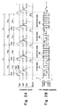
Fig. 2A and 2B constitute a timing chart showing
contents of gate signals and a source signal in the liquid
crystal display device of Fig. 1, wherein Fig. 2A is a
graph showing the gate signals and Fig. 2B is a graph
showing the source signal.
Fig. 3A and Fig. 3B are graphs showing changes in
potential of a pixel electrode in the liquid crystal
display device of Fig. 1, wherein Fig. 3A is the graph
showing the changes in black display, and Fig. 3B is the
graph showing the changes in white display.
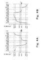
Fig. 4A and 4B are graphs showing changes in
potential of a pixel electrode, wherein Fig. 4A is the
graph showing the changes in the case of switching from
black display to white display in the liquid crystal
display device of Fig. 1, and Fig. 4B is the graph showing
the changes in the case of switching from black display to
white display in a conventional example.
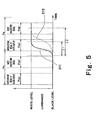
Fig. 5 is a graph showing changes in luminance of
liquid crystals of a certain pixel in the case of
switching from black display to white display.
Fig. 6A and 6B constitute a timing chart showing
contents of gate signals and a source signal in a liquid
crystal display device according to a second embodiment of
the invention, wherein Fig. 6A is a graph showing the gate
signals and Fig. 6B is a graph showing the source signal.
Fig. 7A and 7B constitute a timing chart showing
contents of gate signals and a source signal in a liquid
crystal display device according to a third embodiment of
the invention, wherein Fig. 7A is a graph showing the gate
signals and Fig. 7B is a graph showing the source signal.
Fig. 8A and 8B constitute a timing chart showing
contents of gate signals and a source signal in a liquid
crystal display device according to a fourth embodiment of
the invention, wherein Fig. 8A is a graph showing the gate
signals and Fig. 8B is a graph showing the source signal.
Fig. 9A and 9B constitute a timing chart showing
contents of gate signals and a source signal in a liquid
crystal display device according to a fifth embodiment of
the invention, wherein Fig. 9A is a graph showing the gate
signals and Fig. 9B is a graph showing the source signal.
Fig. 10A and 10B constitute a timing chart showing
contents of gate signals and a source signal in a liquid
crystal display device according to a sixth embodiment of
the invention, wherein Fig. 10A is a graph showing the
gate signals and Fig. 10B is a graph showing the source
signal.
Fig. 11A and 11B constitute a timing chart showing
contents of gate signals and a source signal in a liquid
crystal display device according to a seventh embodiment
of the invention, wherein Fig. 11A is a graph showing the
gate signals and Fig. 11B is a graph showing the source
signal.
Fig. 12A and 12B constitute a timing chart showing
contents of gate signals and a source signal in a
conventional driving method of a liquid crystal display
element, wherein Fig. 12A is a graph showing the gate
signals and Fig. 12B is a graph showing the source signal.
Fig. 13 is a graph showing changes in potential of a
pixel electrode in the case of performing black display in
a conventional liquid crystal display element.
Best Mode for Carrying out the Invention
Hereinafter, the embodiments of the present
invention will be described with reference to the drawings.
First Embodiment
Fig. 1 is a block diagram showing an overall
structure of a control system of a liquid crystal display
device according to the first embodiment of the present
invention.
As shown in Fig. 1, a liquid crystal display device
100 includes a liquid crystal display element 1, a gate
driving circuit 4, and a source driving circuit 6, and a
controller 8.
The liquid crystal element 1 is a known one, and it
is of the active matrix type in this embodiment. The
liquid crystal display element 1 has a TFT substrate (not
shown), a counter substrate (not shown) opposed to the TFT
substrate, and liquid crystals disposed therebetween.
Inside the TFT substrate, a plurality of pixel electrodes
202 are formed in the shape of rows and columns
(hereinafter referred to as matrix), and gate lines 3 and
source lines 5 are disposed for the respective rows and
columns of the pixel electrodes 202 in matrix. A region
occupied by each of the pixel electrodes 202 as viewed
from a direction of a thickness of the liquid crystal
display element (more precisely, of a liquid crystal cell)
is a pixel 2, and a region occupied by the overall pixels
2 is a screen. Each of the pixel electrodes 202 is
connected to a relevant one of the source lines 5 via a
switching element 203 and a relevant one of the gate lines
3 is connected to a gate of the switching element 203.
The switching element 203 is formed by TFT, for example.
Each of the pixels 2 has a common electrode 7a, and all
the common electrodes 7a are electrically connected to one
another and grounded by a common wiring 7. In turn, an
inner face of the counter substrate, a counter electrode
201 is formed. Liquid crystal capacitance is denoted by
Clc. Storage capacitance is denoted by Cst.
The controller 8 supplies a picture signal, which is
input externally, to the source driving circuit 6 and
outputs a control signal to each of the source driving
circuit 6 and the gate driving circuit 4, whereby the
source driving circuit 6 and the gate driving circuit 4
are so controlled as to generate and output source signals
Ss1 to Ssend and gate signals Sg1 to Sgend, respectively.
The gate driving circuit 4 sends the gate signals Sg1 to
Sgend to the switching elements 203 of the pixels 2
respectively via the gate lines 3 to bring the switching
elements to ON state sequentially. The source driving
circuit 6 sends the source signals Ss1 to Ssend to the
pixel electrodes 202 respectively via the source lines 5.
In this case, the source signals Ss1 to Ssend are sent in
accordance with timings of the ON operations of the
switching elements 203 of the pixels 2. Thus, electric
fields respectively corresponding to the source signals
Ss1 to Ssend are generated between the pixel electrodes
202 and the counter electrode 201, and transmittivities of
the liquid crystals changes depending on the thus-generated
electric fields. Accordingly, luminance of
light emitted from a backlight (not shown) is modulated
depending on the changes in transmittivity, and an image
responsive to the source signals Ss1 to Ssend is displayed
on the screen of the liquid crystal element 1.
Next, constitution of the gate driving circuit 4 and
the source driving circuit 6 will be described in detail.
Figs. 2A and 2B constitute a timing chart showing contents
of gate signals and a source signal in the liquid crystal
display device of Fig. 1, wherein Fig. 2A is a graph
showing the gate signals and Fig. 2B is a graph showing
the source signal.
Referring to Figs. 1, 2A, and 2B, the source driving
circuit 6 is so constituted as to generate and output the
source signals Ss1 to Ssend which are characteristic of
this embodiment as shown in Fig. 2B. Though a source
signal Ssn which is selected arbitrarily among the source
signals Ss1 to Ssend output for the respective gate lines
5 is shown in Fig. 2B, the other source signals are
similar to the source signal Ssn. The source signal Ssn
is sectioned as to correspond to each frame. An odd frame
period is denoted by Po, and an even frame period is
denoted by Pe. Each of the frame periods Po and Pe is
bisectioned into two write periods which are a first write
period Poa for writing a picture signal to all the pixels
2 in one column and a second write period Pob for writing
a non-picture signal in the same manner. Accordingly, the
source signal Ssn is constituted of the picture signal 101
for the first write period Poa and the non-picture signal
102 for the second write period Pob. Further, the first
write period Poa and the second write period Pob are
divided into periods Poa' (hereinafter referred to as
pixel write periods) for writing the picture signal to
each of the pixels 2 in one column and pixel write periods
Pob' for writing the non-picture signal to each of the
pixels in one column, respectively. The source signal Ssn
has voltage values corresponding to predetermined display
gradations for the respective pixel write periods Poa' and
Pob'. In the source signal Ssn, a polarity is alternated
in order to AC drive the liquid crystal element 1. The
polarity is reversed every pixel write period (Poa', Pob'),
and every frame period (Po, Pe). Also polarities of the
first write period Poa during which the picture signal 101
is written and the second write period Pob during which
the non-picture signal 102 is written are reversed from
each other. Therefore, a polarity of a non-picture signal
write period (Pob in the drawing) in a certain frame
period is identical to that of a picture signal write
period (Pea in the drawing) in a succeeding frame period.
As used herein, VsB(+) and VsB(-) are voltage values for
black display, and Vsup(+) and Vsup(-) are voltage values
for non-picture signals.
The gate driving circuit 4 is so constituted as to
generate and output the gate signals Sg1 to Sgend which
are similar to those of the conventional example. Each of
the gate signals Sg1 to Sgend is a binary signal which has
a voltage Vgon at a high level (hereinafter referred to as
H level) and a voltage of Vgoff at a low level
(hereinafter referred to as L level), and becomes the H
level during the pixel write periods Poa', Pob', Pea', and
Peb' of the relevant pixels 2 while becomes the L level
during remaining retention periods Poa", Pob", Pea", and
Peb". Therefore, each of the gate signals Sg1 to Sgend
becomes the H level twice in each of the frame periods Po
and Pe; once in each of the first write periods Poa and
Pea and once in each of the second write periods Pob and
Peb. Thus, when the gate signals Sg1 to Sgend are output,
switching elements 203 of the pixels 2 are turned on row
by row sequentially during the respective pixel write
periods Poa', Pob', Pea', and Peb'. During each of the ON
periods, the picture signal 101 and the non-picture signal
102 of each of the source signals Ss1 to Ssend
corresponding to each of the pixels 2 are written.
Next, operation of the thus-constituted liquid
crystal display device (a driving method of the liquid
crystal display element) will be described with reference
to Figs. 1 to 5B. Figs. 3A and Fig. 3B are graphs showing
changes in potential of a certain pixel electrode in the
liquid crystal display device of Fig. 1, wherein Fig. 3A
is the graph showing the changes in black display, and Fig.
3B is the graph showing the changes in white display. Fig.
4A and 4B are graphs showing changes in potential of a
pixel electrode, wherein Fig. 4A is the graph showing the
changes in the case of switching from black display to
white display in the liquid crystal display device of Fig.
1, and Fig. 4B is the graph showing the changes in the
case of switching from black display to white display in
the conventional example. Fig. 5 is a graph showing
changes in luminance of liquid crystals of a certain pixel
in the case of switching from black display to white
display.
In this embodiment, the normally white mode is
employed. The voltage Vgon at the H level of the gate
signal Ssn is set at 15 V, and the voltage Vgoff at the L
level of the signal Ssn is set at -10 V. An amplitude of
the source signal Ssn is set with respect to the potential
of the counter electrode 201 in such a manner that: the
voltages Vsup(+) and Vsup(-) for the non-picture signal
are +6 V and -6 V, respectively; VsB(+) and VsB(-) for the
black display level are +5 V and -5 V, respectively; and
VsW(+) and VsW(-) for the white display level are +1 V and
- 1 V, respectively, and a duration of each of the frame
periods is 16.6 ms (60 Hz). Further, a response in an
arbitrary pixel 2 in the fist row among the pixels in
matrix is described by way of example.
Referring to Figs. 1 to 5B, a case of black display
of a certain pixel 2 of the liquid crystal element 1 will
be described. In this case, as shown in Fig. 3A, the
picture signal 101 of the black display level of the
source signal is input during the pixel write period Poa'
of the first write period Poa of an odd frame Po. Then,
in accordance with a discharge characteristic which
depends on the capacitance of the pixel 2, the potential
of the pixel electrode 202 is changed from +6 V which is
the voltage value Vsup(+) of the non-picture signal 102 of
the preceding frame period to +5 V which is the black
display level VsB(+). The value is retained during the
retention period Poa". After that, the non-picture signal
102 is input during the pixel write period Pob' of the
second write period Pob. In this case, since the non-picture
signal 102 has a polarity opposite to that of the
picture signal 101, the potential of the pixel electrode
202 is changed from +5 V to -6 V which is the voltage
value Vsup(-) of the non-picture signal. The value is
retained during the retention period Pob". Then, the
picture signal 101 of the white level of the source signal
Ssn is input during the pixel write period Pea' of the
first write period Poa of the succeeding odd frame Pe. In
this case, since the picture signal has the same polarity
with the non-picture signal 102 of the preceding frame,
the potential of the pixel electrode 202 is changed from
-6 V to -5 V which is the white display level VsW in
accordance with a charge characteristic which depends on
the capacity of the pixel 2. The value is retained during
the retention period Pea". Then, the non-picture signal
102 is input during the pixel write period Peb' of the
second write period Peb. In this case, the non-picture
signal 102 has a polarity opposite to that of the picture
signal 101, the potential of the pixel electrode 202 is
changed from -5 V to +6 V which is the voltage value
Vsup(+) of the non-picture signal 102. The value is
retained during the retention period Peb" (not shown).
As described above, according to this embodiment, at
the time when the non-picture signal 102 is written to the
pixel 2 and, after that, the picture signal 101 in the
succeeding frame period is written to the pixel 2, the
polarities of the non-picture signal 102 and the picture
signal 101 are identical to each other. Therefore, it is
possible to reduce the potential difference to be written,
and, in this example, the potential difference is reduced
to about 1 V. Consequently, it is possible to perform the
writing of the picture signal 101 with a liberal allowance
of time.
The above operation will hereinafter be compared
with the conventional example shown in Fig. 13. In the
conventional example, waveforms and potentials of gate
signals Sg1 to Sgend and a source signal Ssn are the same
as those of the present embodiment. As a result, when
performing the black display, a potential difference of
writing the picture signal 101 during a frame period after
writing the non-picture signal 102 is about 11 V in each
of the odd frame period Po and the even frame period Pe,
and it is impossible to write a sufficient potential
required for performing the black display to the pixel
electrode 202, resulting in display unevenness of the
liquid crystal display device.
In addition, it is necessary to perform the signal
writing with respect to the potential difference of about
11 V when writing the non-picture signal 102 after writing
the picture signal 101 also in this embodiment; however,
the writing is performed without any trouble as shown in
Fig. 3A. Further, since the non-picture signal 102 is
essentially used for the purpose of preventing the reverse
transition, it is not problematic at all from the
practical standpoint if the potential of the pixel
electrode 202 was not transitioned perfectly to the
predetermined potential in the write period so far as the
potential is close to the predetermined potential. In
view of this, the black display performed in accordance
with this embodiment is failsafe.
Next, the white display of the pixel 2 of the liquid
crystal element 1 will be described. In this case, as
shown in Fig. 3B, the picture signal 101 is input during
the pixel write period Poa' of the first write period Poa
of the even frame Po. Then, a potential of the pixel
electrode 202 changes from +6 V which is the voltage value
Vsup(+) of the non-picture signal 102 in the preceding
frame period to +1 V which is the white display level
VsW(+). The value is retained during the retention period
Poa". Then, the non-picture signal 102 is input during
the pixel write period Pob' of the second write period Pob.
The potential of the pixel electrode 202 then changes from
+1 V to -6 V which is the voltage value Vsup(-) of the
non-picture signal 102. The value is retained during the
retention period Pob". Then, the picture signal 101 of
the white display level of the source signal Ssn is input
during the pixel write period Pea of the first write
period Poa of the next even frame Pe. Then, the potential
of the pixel electrode changes from -6 V to -1 V which is
the white display level VsW(-). The value is retained
during the retention period Pea". Next, the non-picture
signal 102 is input during the pixel write period Peb' of
the second write period Peb. Then, the potential of the
pixel electrode 202 changes from -5 V to +6 V which is the
voltage Vsup(+) of the non-picture signal 102. The value
is retained during the retention period Peb" (not shown).
The above-described white display is the case of
performing the white display under the worst conditions in
this embodiment; however, even in this worst case, it is
possible to suppress the potential difference when writing
the picture signal 101 after writing the non-picture
signal 102 to about 5 V, and the signal writing is
performed without any trouble.
In addition, in the case of performing the white
display, a response speed is slowed down since the liquid
crystals transition to the white display state owing to
relaxation; therefore, the liquid crystals may in some
cases fail to perfectly transition to the white display
state even when the potential difference is smaller than
that of the black display. In this embodiment, since the
potential difference in writing the picture signal is 5 V,
as described above, which is smaller than that (7 V)
achieved by the conventional example (see Fig. 4B), the
white display is performed without any trouble.
Further, referring to Figs. 3A and 3B, after writing
the source signal Ssn to the pixel 2, a pixel voltage drop
called a punch-through voltage occurs in actuality due to
a coupling of the capacity of the switching element 203
and the pixel capacity at the time point when the gate
signal falls to bring the switching element 203 to the OFF
state; however, explanation for such pixel voltage drop is
omitted in order to simplify the description.
Next, a case of switching from the black display to
the white display will be described. Figs. 4A and 4B are
graphs showing changes in potential of a certain pixel
electrode in the case of switching from the black display
to the white display, wherein Fig. 4A is the graph showing
the changes in this embodiment, and Fig. 4B is the graph
showing the changes in the conventional example.
As shown in Fig. 4B, when switching from the black
display to the white display in the conventional example,
the non-picture signal 102 of the preceding frame period
(the odd frame period Po in Fig. 4B) has a polarity
opposite to that of the picture signal 101 of the white
display of the succeeding frame period (the even frame
period Pe in Fig. 4B) and has a larger voltage to be
applied to liquid crystals. In turn, in this embodiment,
when switching from the black display to the white display,
the non-picture signal 102 of the preceding frame period
(the odd frame period Po in Fig. 4A) has the same polarity
as the picture signal 101 of the white display of the
succeeding frame period (the even frame period Pe in Fig.
4A) and has a larger voltage to be applied to liquid
crystals. Therefore, in this embodiment, the liquid
crystals operate more rapidly as compared with the
conventional example owing to the identical polarity of
the non-picture signal 102 and the picture signal 101, and,
as a result, a response speed of the liquid crystals is
improved. This effect is shown in Fig. 5. Fig. 5 is a
graph showing changes in luminance of a liquid crystal
display device with respect to time in the case of
switching from the black display to the white display. In
Fig. 5, the reference numeral 211 denotes a luminance
change curve with respect to time of the liquid crystal
display device according to this embodiment, and the
reference numeral 212 denotes a luminance change curve
with respect to time of the conventional liquid crystal
display device. Referring to Fig. 5, the response speed
of the liquid crystals with respect to the switching from
the black display to the white display of the liquid
crystal display device according to this embodiment, i.e.
the time τ1 required for the luminance to transition from
a black level to a white level, is shorter than a response
speed τ2 of liquid crystals of the conventional liquid
crystal display device.
As described in the foregoing, in this embodiment,
the liquid crystal display without unevenness on the whole
screen is realized, and the effect of improving the
response speed is achieved.
If the potential of the pixel electrode 202 fails to
reach the desired one in writing the picture signal 101,
such failure results in the display unevenness; however,
it is possible to achieve the reverse transition
prevention effect sufficiently as far as the voltage
having the predetermined value or more is applied to the
liquid crystals in writing the non-picture signal 102 even
if the potential of the pixel electrode 202 dose not reach
the set voltage Vsup. Further, in the case of attaining
sharpness of dynamic images by inserting the black display
per frame period, sufficient sharpness of dynamic images
is achieved as far as the black level is displayed during
writing the picture signal 101 even if the non-picture
signal 102 at the time of the black insertion does not
exactly reach the potential of black display. Therefore,
the voltage Vsup may be set to a value identical to the
black display potential.
Further, though the non-picture signal is written
after writing the picture signal in each of the frame
periods in this embodiment, the non-picture signal may be
written before writing the picture signal. In this case,
the similar effect is achieved by setting the polarities
of the picture signal and the non-picture signal identical
to each other in the frame period. Also, though the
retention period after writing the picture signal and the
retention period after writing the non-picture signal are
identical in duration in this embodiment, the durations
are not critical and may be different from each other. In
that case, the display brightness, the reverse transition
prevention effect, the sharpness of dynamic images, and
the like are changed, but, in both of the cases, the
signal writing ability is improved, and the display
unevenness is suppressed.
Second Embodiment
Fig. 6A and 6B constitute a timing chart showing
contents of gate signals and a source signal in a liquid
crystal display device according to the second embodiment
of the invention, wherein Fig. 6A is a graph showing the
gate signals and Fig. 6B is a graph showing the source
signal. In Figs. 6A and 6B, the reference numerals
identical to those of Figs. 2A and 2B denote components
identical or equivalent to those of Figs. 2A and 2B.
As shown in Fig. 6A and 6B, unlike the first
embodiment, a polarity of the picture signal 101 of the
source signal Ssn remains unchanged during each of frame
periods Po and Pe and a polarity of a non-picture signal
102 remains unchanged during each of the frame periods Po
and Pe in this embodiment. Other parts of constitution
are the same as the first embodiment.
With such constitution, an amplitude of the source
signal Ssn during the write periods Poa and Pea of the
picture signal 101 and the write periods Pob and Peb of
the non-picture signal 102 is reduced. Therefore, it is
possible to reduce time required for a potential of the
source signal to reach a desired signal potential of each
of pixels and to suppress influence of signal delay due to
resistance in source lines 5 and parasitic capacitance.
Thus, signal writing ability is further improved. Further,
a load on the driving circuit 6 for supplying the source
signal Ssn is reduced.
Third Embodiment
Fig. 7A and 7B constitute a timing chart showing
contents of gate signals and a source signal in a liquid
crystal display device according to a third embodiment of
the invention, wherein Fig. 7A is a graph showing the gate
signals and Fig. 7B is a graph showing the source signal.
In Figs. 7A and 7B, the reference numerals identical to
those of Figs. 2A and 2B denote components identical or
equivalent to those of Figs. 2A and 2B.
As shown in Fig. 7A and 7B, unlike the first
embodiment, each of the pixel write periods Poa' and Pea'
of the picture signal 101 is provided twice in each of the
frame periods Po and Pe in this embodiment. In this case,
the picture signal 101 to be written to the pixel is
actually written in each of the latter pixel write periods.
Other parts of constitution are the same as the first
embodiment.
With such constitution, the write period for the
picture signal 101 is effectively increased, thereby
further improving the ability of writing the picture
signal 101.
Fourth Embodiment
Fig. 8A and 8B constitute a timing chart showing
contents of gate signals and a source signal in a liquid
crystal display device according to a fourth embodiment of
the invention, wherein Fig. 8A is a graph showing the gate
signals and Fig. 8B is a graph showing the source signal.
In Figs. 8A and 8B, the reference numerals identical to
those of Figs. 2A and 2B denote components identical or
equivalent to those of Figs. 2A and 2B.
As shown in Figs. 8A and 8B, each of the pixel write
periods of the picture signal 101 and the non-picture
signal 102 is provided twice consecutively in each of the
frame periods Po and Pe. In other words, a length of each
of the pixel write periods of the picture signal and the
non-picture signal is twice that of the first embodiment.
In this case, the picture signal 101 to be written to the
pixel is actually written in each of the latter pixel
write periods Poa' and Pea'. Other parts of constitution
are the same as the first embodiment.
With such constitution, falling and rising periods
of the picture signal 101 are reduced as compared with the
third embodiment, thereby further increasing a substantial
write period for the picture signal 101. Therefore, the
ability of writing the picture signal 101 is further
improved as compared with the third embodiment.
Fifth Embodiment
Figs. 9A and 9B constitute a timing chart showing
contents of gate signals and a source signal in a liquid
crystal display device according to a fifth embodiment of
the invention, wherein Fig. 9A is a graph showing the gate
signals and Fig. 9B is a graph showing the source signal.
In Figs. 9A and 9B, the reference numerals identical to
those of Figs. 2A and 2B denote components identical or
equivalent to those of Figs. 2A and 2B.
The liquid crystal display device of this embodiment
is capable of color display, and the overall constitution
is as follows. The liquid crystal display device is
different from the liquid crystal display device of the
first embodiment in that a light source of backlight (not
shown) has a cool cathode tube (not shown) capable of
emitting light respectively for red (hereinafter
abbreviated to R), green (hereinafter abbreviated to G),
and blue (hereinafter abbreviated to blue); a circuit (not
shown) for controlling timings of the light emission is
provided; and a controller 8, a gate driving circuit 4,
and a source driving circuit 6 same as those shown in Fig.
1 output a control signal, a gate signal, and a source
signal, respectively, in a way of sectioning a frame
period according to R, G, and B. Other parts of the
constitution are the same as the liquid crystal display
device of the first embodiment. Since the overall
constitution is known, the detailed description therefor
is omitted.
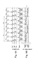
Specifically, as shown in Figs. 9A and 9B, the
liquid crystal display device of this embodiment divides
each of the frame periods Po and Pe into a first, a second,
and a third write periods (Poa, Pea), (Pob, Peb), and (Poc,
Pec) in the field sequential driving, and a picture signal
for R (hereinafter referred to as R picture signal) 101R,
a picture signal for G (hereinafter referred to as G
picture signal) 101G, and a picture signal for B
(hereinafter referred to as B picture signal) 101B are
written respectively in the first, the second, and the
third write periods (Poa, Pea), (Pob, Peb), and (Poc, Pec).
A pixel write period for the R picture signal 101R, a
pixel write period for the G picture signal 101G, and a
pixel write period for the B picture signal 101B in the
odd frame period Po are denoted by Poa', Pob', and Poc'.
A pixel write period for the R picture signal 101R, a
pixel write period for the G picture signal 101G, and a
pixel write period for the B picture signal 101B in the
even frame period Pe are denoted by Pea', Peb', and Pec'.
A polarity of each of the picture signals 101R, 101G, and
101B is unchanged during each of the picture signal write
periods Poa, Pob, Poc, Pea, Peb, and Pec, and the polarity
is reversed every two consecutive picture signal write
periods.
With such constitution, the polarity is reversed
only once during each of the frame periods Po and Pe in
writing the picture signals 101R, 101G, and 101B to the
pixel, thereby reducing a potential difference to be
written in the case where the polarity is not reversed.
Thus, the writings of the picture signals 101R, 101G, and
101B are facilitated. Also, since an amplitude of the
source signal is reduced, deterioration in writing ability
otherwise caused by a delay in the source signal Ssn is
suppressed. Further, since the polarity of the source
signal Ssn changes at least once in each of the frame
periods Po and Pe, an effect of reducing flickering and
burn-in in displaying a picture is achieved. In view of
the above results, this embodiment enables color display
without unevenness in a whole image on the screen.
Sixth Embodiment
Figs. 10A and 10B constitute a timing chart showing
contents of gate signals and a source signal in a liquid
crystal display device according to a sixth embodiment of
the invention, wherein Fig. 10A is a graph showing the
gate signals and Fig. 10B is a graph showing the source
signal. In Figs. 10A and 10B, the reference numerals
identical to those of Figs. 9A and 9B denote components
identical or equivalent to those of Figs. 9A and 9B.
Unlike the fifth embodiment, the liquid crystal
display device of this embodiment has the following
constitution. That is, each of the frame periods Po and
Pe is divided into four write periods of first to fourth
write periods (Poa, Pea), (Pob, Peb), (Poc, Pec), and (Pod,
Ped), and an R picture signal 101R, a G picture signal
101G, a B picture signal 101B, and a non-picture signal
102 are written in the first to fourth write periods (Poa,
Pea), (Pob, Peb), (Poc, Pec), and (Pod, Ped), respectively.
A polarity of each of the picture signals 101R, 101G, and
101B, and the non-picture signal 102 is reversed every
pixel write period Poa', Pob', Poc', Pod', Pea', Peb',
Pec', and Fed' and every picture signal write period Poa,
Pob, Poc, Pea, Peb, Pec. Further, the Polarity of the
non-picture signal 102 of the preceding frame period is
identical to that of the initial picture signal 101R in
the succeeding frame period. Other parts of the
constitution are the same as the fifth embodiment.
With such construction, in the case of using the
liquid crystal mode performing the bend transition, it is
possible to prevent the reverse transition to the splay
orientation in the field sequential driving because the
non-picture signal 102 is also written, and color display
without unevenness in a whole image on the screen is
realized because the polarity of the non-picture signal
102 of the preceding frame period is the same as that of
the picture signal 101 of the succeeding frame period.
Seventh Embodiment
Fig. 11A and 11B constitute a timing chart showing
contents of gate signals and a source signal in a liquid
crystal display device according to a seventh embodiment
of the invention, wherein Fig. 11A is a graph showing the
gate signals and Fig. 11B is a graph showing the source
signal. In Figs. 11A and 11B, the reference numerals
identical to those of Figs. 10A and 10B denote components
identical or equivalent to those of Figs. 10A and 10B.
In this embodiment, unlike the sixth embodiment, a
polarity of each of the picture signals 101R, 101G, 101B
and the non-picture signal 102 is unchanged during each of
picture signal write periods Poa, Pob, Poc, Pea, Peb, and
Pec, and the polarity is reversed every four write periods
including three picture signal write periods and one non-picture
write period during consecutive two frame periods
Po and Pe. As a result, the polarity of the non-picture
signal 102 of the preceding frame period is the same as
that of the initial picture signal 101R of the succeeding
frame period. Other parts of the constitution are the
same as the sixth embodiment.
With such constitution, too, it is possible to
prevent the reverse transition to the splay orientation in
the field sequential driving, and color display without
unevenness in a whole image on the screen is realized as
in the sixth embodiment.
From the foregoing description, many modification
and other embodiments will be apparent to those skilled in
the art. Therefore, it should be understood that the
above description is given by way of example and for the
purpose of teaching the best mode for carrying out the
invention to those skilled in the art. Details of the
constitution and/or the function of the invention can be
substantially changed without departing from the sprit of
the invention.
Industrial Applicability
The liquid crystal display device of the present
invention is useful as household and industrial thin image
display devices.
The driving method of liquid crystal display element
of the invention is useful as household and industrial
thin image display devices.