EP1422618A2 - Coprocesseur VLIW en grappe avec un bus inter-cluster dynamiquement reconfigurable à temps d'exécution - Google Patents
Coprocesseur VLIW en grappe avec un bus inter-cluster dynamiquement reconfigurable à temps d'exécution Download PDFInfo
- Publication number
- EP1422618A2 EP1422618A2 EP03257332A EP03257332A EP1422618A2 EP 1422618 A2 EP1422618 A2 EP 1422618A2 EP 03257332 A EP03257332 A EP 03257332A EP 03257332 A EP03257332 A EP 03257332A EP 1422618 A2 EP1422618 A2 EP 1422618A2
- Authority
- EP
- European Patent Office
- Prior art keywords
- interconnect
- processor
- program
- coprocessor
- processing system
- Prior art date
- Legal status (The legal status is an assumption and is not a legal conclusion. Google has not performed a legal analysis and makes no representation as to the accuracy of the status listed.)
- Withdrawn
Links
- 238000012545 processing Methods 0.000 claims abstract description 71
- 238000000034 method Methods 0.000 claims description 16
- 230000007246 mechanism Effects 0.000 claims description 12
- 230000008878 coupling Effects 0.000 claims 9
- 238000010168 coupling process Methods 0.000 claims 9
- 238000005859 coupling reaction Methods 0.000 claims 9
- 238000004891 communication Methods 0.000 description 9
- 230000008569 process Effects 0.000 description 6
- 238000012546 transfer Methods 0.000 description 6
- 230000006870 function Effects 0.000 description 5
- 239000004744 fabric Substances 0.000 description 4
- 230000009466 transformation Effects 0.000 description 4
- XUIMIQQOPSSXEZ-UHFFFAOYSA-N Silicon Chemical compound [Si] XUIMIQQOPSSXEZ-UHFFFAOYSA-N 0.000 description 3
- 230000008901 benefit Effects 0.000 description 3
- 229910052710 silicon Inorganic materials 0.000 description 3
- 239000010703 silicon Substances 0.000 description 3
- 238000013459 approach Methods 0.000 description 2
- 230000001105 regulatory effect Effects 0.000 description 2
- 230000011664 signaling Effects 0.000 description 2
- 238000000844 transformation Methods 0.000 description 2
- 235000008694 Humulus lupulus Nutrition 0.000 description 1
- 230000004075 alteration Effects 0.000 description 1
- 238000003491 array Methods 0.000 description 1
- 230000005540 biological transmission Effects 0.000 description 1
- 230000008859 change Effects 0.000 description 1
- 238000010276 construction Methods 0.000 description 1
- 230000001276 controlling effect Effects 0.000 description 1
- 230000007812 deficiency Effects 0.000 description 1
- 230000001419 dependent effect Effects 0.000 description 1
- 238000013461 design Methods 0.000 description 1
- 230000000694 effects Effects 0.000 description 1
- 230000008030 elimination Effects 0.000 description 1
- 238000003379 elimination reaction Methods 0.000 description 1
- 238000005516 engineering process Methods 0.000 description 1
- 230000006872 improvement Effects 0.000 description 1
- 230000006698 induction Effects 0.000 description 1
- 230000000977 initiatory effect Effects 0.000 description 1
- 230000003993 interaction Effects 0.000 description 1
- 238000013507 mapping Methods 0.000 description 1
- 230000004048 modification Effects 0.000 description 1
- 238000012986 modification Methods 0.000 description 1
- 239000004065 semiconductor Substances 0.000 description 1
- 101150000485 snd1 gene Proteins 0.000 description 1
- 238000006467 substitution reaction Methods 0.000 description 1
Images


Classifications
-
- G—PHYSICS
- G06—COMPUTING; CALCULATING OR COUNTING
- G06F—ELECTRIC DIGITAL DATA PROCESSING
- G06F9/00—Arrangements for program control, e.g. control units
- G06F9/06—Arrangements for program control, e.g. control units using stored programs, i.e. using an internal store of processing equipment to receive or retain programs
- G06F9/30—Arrangements for executing machine instructions, e.g. instruction decode
- G06F9/38—Concurrent instruction execution, e.g. pipeline, look ahead
- G06F9/3885—Concurrent instruction execution, e.g. pipeline, look ahead using a plurality of independent parallel functional units
-
- G—PHYSICS
- G06—COMPUTING; CALCULATING OR COUNTING
- G06F—ELECTRIC DIGITAL DATA PROCESSING
- G06F15/00—Digital computers in general; Data processing equipment in general
- G06F15/76—Architectures of general purpose stored program computers
- G06F15/80—Architectures of general purpose stored program computers comprising an array of processing units with common control, e.g. single instruction multiple data processors
- G06F15/8007—Architectures of general purpose stored program computers comprising an array of processing units with common control, e.g. single instruction multiple data processors single instruction multiple data [SIMD] multiprocessors
- G06F15/8015—One dimensional arrays, e.g. rings, linear arrays, buses
-
- G—PHYSICS
- G06—COMPUTING; CALCULATING OR COUNTING
- G06F—ELECTRIC DIGITAL DATA PROCESSING
- G06F9/00—Arrangements for program control, e.g. control units
- G06F9/06—Arrangements for program control, e.g. control units using stored programs, i.e. using an internal store of processing equipment to receive or retain programs
- G06F9/30—Arrangements for executing machine instructions, e.g. instruction decode
- G06F9/30098—Register arrangements
- G06F9/3012—Organisation of register space, e.g. banked or distributed register file
-
- G—PHYSICS
- G06—COMPUTING; CALCULATING OR COUNTING
- G06F—ELECTRIC DIGITAL DATA PROCESSING
- G06F9/00—Arrangements for program control, e.g. control units
- G06F9/06—Arrangements for program control, e.g. control units using stored programs, i.e. using an internal store of processing equipment to receive or retain programs
- G06F9/30—Arrangements for executing machine instructions, e.g. instruction decode
- G06F9/38—Concurrent instruction execution, e.g. pipeline, look ahead
- G06F9/3824—Operand accessing
- G06F9/3826—Bypassing or forwarding of data results, e.g. locally between pipeline stages or within a pipeline stage
- G06F9/3828—Bypassing or forwarding of data results, e.g. locally between pipeline stages or within a pipeline stage with global bypass, e.g. between pipelines, between clusters
-
- G—PHYSICS
- G06—COMPUTING; CALCULATING OR COUNTING
- G06F—ELECTRIC DIGITAL DATA PROCESSING
- G06F9/00—Arrangements for program control, e.g. control units
- G06F9/06—Arrangements for program control, e.g. control units using stored programs, i.e. using an internal store of processing equipment to receive or retain programs
- G06F9/30—Arrangements for executing machine instructions, e.g. instruction decode
- G06F9/38—Concurrent instruction execution, e.g. pipeline, look ahead
- G06F9/3836—Instruction issuing, e.g. dynamic instruction scheduling or out of order instruction execution
- G06F9/3853—Instruction issuing, e.g. dynamic instruction scheduling or out of order instruction execution of compound instructions
-
- G—PHYSICS
- G06—COMPUTING; CALCULATING OR COUNTING
- G06F—ELECTRIC DIGITAL DATA PROCESSING
- G06F9/00—Arrangements for program control, e.g. control units
- G06F9/06—Arrangements for program control, e.g. control units using stored programs, i.e. using an internal store of processing equipment to receive or retain programs
- G06F9/30—Arrangements for executing machine instructions, e.g. instruction decode
- G06F9/38—Concurrent instruction execution, e.g. pipeline, look ahead
- G06F9/3877—Concurrent instruction execution, e.g. pipeline, look ahead using a slave processor, e.g. coprocessor
- G06F9/3879—Concurrent instruction execution, e.g. pipeline, look ahead using a slave processor, e.g. coprocessor for non-native instruction execution, e.g. executing a command; for Java instruction set
-
- G—PHYSICS
- G06—COMPUTING; CALCULATING OR COUNTING
- G06F—ELECTRIC DIGITAL DATA PROCESSING
- G06F9/00—Arrangements for program control, e.g. control units
- G06F9/06—Arrangements for program control, e.g. control units using stored programs, i.e. using an internal store of processing equipment to receive or retain programs
- G06F9/30—Arrangements for executing machine instructions, e.g. instruction decode
- G06F9/38—Concurrent instruction execution, e.g. pipeline, look ahead
- G06F9/3885—Concurrent instruction execution, e.g. pipeline, look ahead using a plurality of independent parallel functional units
- G06F9/3889—Concurrent instruction execution, e.g. pipeline, look ahead using a plurality of independent parallel functional units controlled by multiple instructions, e.g. MIMD, decoupled access or execute
- G06F9/3891—Concurrent instruction execution, e.g. pipeline, look ahead using a plurality of independent parallel functional units controlled by multiple instructions, e.g. MIMD, decoupled access or execute organised in groups of units sharing resources, e.g. clusters
Definitions
- the present invention is directed, in general, to runtime reconfigurable processors and, more specifically, to a combination of clustered very large instruction word and runtime reconfigurable architectures that provides performance, in terms of power dissipation and processing speed, comparable to hardwired accelerators on a programmable platform.
- VLIW very large instruction word
- FPGAs field programmable gate arrays
- ILP instruction level parallelism
- Embedded multimedia applications exhibit high ILP--as much as 10 to 100 instructions per cycle--in a small fraction of the total program code, often quoted as 10-20%, and low ILP--about 2--in the rest of the program, the remaining 80-90%.
- the high ILP portion of the program code e.g., the loops
- VLIW and superscalar architectures which can issue several instructions simultaneously or for concurrent execution, have been proposed to accelerate code with high ILP.
- issue width increases, mounting design constraints--primarily related to timing--on the register file have led to clustered architectures where the registers are split among several physically distinct files around which execution units are clustered.
- An inter-cluster bus is also added to enable data transfer between register files.
- significant silicon overhead and performance penalty is incurred by the inter-cluster bus necessary for transferring data between register files.
- program size overhead is also incurred due to the addition of send/receive instructions to transfer data between register files.
- the inter-cluster bus overhead effectively limits the number of clusters to about four. Assuming each cluster has an issue width of four instructions, the maximum issue width of this architecture is sixteen, a typical upper limit for clustered VLIW machines.
- clustered VLIW architectures incur a significant power dissipation penalty compared to a fixed hardware implementation because of the inter-cluster bus and because of the unused clusters when the ILP of the program code is too small.
- a clustered architecture ideally has too little parallelism for the high ILP sections of the code and too much for the remainder of the code.
- the poor programming model is a consequence of the absence of virtualization of the computing resources. This refers to the number of computing resources (arithmetic logic units, multipliers, etc.) that are typically visible in the programming abstraction. The consequence is that a program segment requiring more resources than are available cannot be accelerated on the RRCP.
- reconfiguration phases also generally show up in the programming model, adding to the complexity of the programming model.
- RRCPs RRCPs
- Additional drawbacks of RRCPs include the significant amount of time taken by reconfiguration, the amount of resources dedicated to reconfiguration (such as a reconfiguration bitstream cache), the use of Register Transfer Level (RTL) or dedicated languages to program reconfiguration resources, and the area required and performance penalty incurred by reconfigurable logic.
- RTL Register Transfer Level
- clustered VLIW processing elements each preferably simple and identical, coupled by a runtime reconfigurable inter-cluster interconnect to form a coprocessor executing only those portions of a program having high instruction level parallelism.
- the initial portion of each program segment executed by the coprocessor reconfigures the interconnect, if necessary, or is skipped.
- Clusters may be directly connected to a subset of neighboring clusters, or indirectly connected to any other cluster, a hierarchy exposed to the programming model and enabling a larger number of clusters to be employed.
- the coprocessor is idled during remaining portions of the program to reduce power dissipation.
- FIGURES 1 through 9 discussed below, and the various embodiments used to describe the principles of the present invention in this patent document are by way of illustration only and should not be construed in any way to limit the scope of the invention. Those skilled in the art will understand that the principles of the present invention may be implemented in any suitably arranged device.
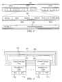
- FIGURE 1 depicts a processing system employing a clustered VLIW architecture with a runtime reconfigurable inter-cluster bus according to one embodiment of the present invention.
- Processing system 100 in the exemplary embodiment executes a program and includes a general-purpose processor or central processing unit (CPU) 101 communicably coupled to a coprocessor 102 via communication mechanism 103--e.g., a set of signal lines between processor 101 and a processor interface 104 within coprocessor 102.
- processor 101 transmits instructions and operand data to the coprocessor 102 via communication mechanism 103 for execution by the coprocessor 102, and receives (or retrieves) results of such instructions from the coprocessor 102.
- processor interface 104 includes a first-in, first-out (FIFO) mechanism 105 used to transfer data between processor 101 and coprocessor 102 and allowing simultaneous and asynchronous operation as described in further detail below in connection with FIGURE 6.
- FIFO first-in, first-out
- processing system 100 includes an instruction cache 106 and a data cache subsystem 107. Although depicted as separate from processor core 101, one or both of instruction cache 106 and data cache subsystem 107 may be fully integrated with processor core 101, and both are preferably at least formed within the same integrated circuit die as processor core 101.
- a memory interface 108 within coprocessor 102 is connected to data cache subsystem 107, where processor 101 and coprocessor 102 share access to data cache subsystem 107 in the exemplary embodiment of FIGURE 1.
- Processor 101 and coprocessor 102 preferably implement means to guarantee data consistency during program execution.
- Coprocessor 102 includes a plurality of VLIW execution clusters 109a-109n executing computational and data intensive loops in the application code for the program executed by the processing system 100.
- Clusters 109a-109n are coupled by a runtime reconfigurable bus or interconnect 110, forming a fabric of programmable computing elements and a runtime reconfigurable interconnect.
- Coprocessor 102 is particularly adept at executing software pipelined loops.
- each connection box 111a-111n connects a number of read and write ports of the cluster's register file 112a-112n to a number of routing resources provided by reconfigurable inter-cluster bus 105, as described in further detail below in connection with FIGURE 4.
- each cluster register file 112a-112n has two write ports and two read ports connected to inter-cluster bus 110.
- Each cluster 109a-109n also includes an arithmetic logic unit (ALU) 113a-113n and a load/store (LD/ST) unit 114a-114n for issuing memory accesses.
- ALU arithmetic logic unit
- LD/ST load/store
- Memory access instructions issued by clusters 109a-109n are collected and prioritized by memory interface 108.
- Processor 101 and coprocessor 102 have distinct program memory subsystems, with processor (core) 101 having a traditional instruction cache 106 as noted above while coprocessor 102 has a separate very wide program memory or instruction cache 115.
- Coprocessor 102 also includes an instruction fetch and dispatch unit 116 retrieving instructions from coprocessor program memory 115 and dispatching them to clusters 109a-109n for execution. Since coprocessor 102 is specialized to execute loops, loop control hardware 117 is included within the instruction fetch and dispatch unit 116 of coprocessor 102 to reduce the number of conditional branches executed in the loop body, possibly to zero, thus improving performance by removing latencies typically associated with taken branches. Loop control hardware 117 is initialized prior to loop execution in accordance with techniques well-known in digital signal processing (DSP) architectures.
- DSP digital signal processing
- a clock divider 118 for coprocessor 102 derives the coprocessor clock from the core clock driving the remainder of processing system 100.
- the coprocessor clock generated by clock divider 118 is controller by processor 101 (through processor interface 104) as described in copending U.S. Patent Application Serial No. 10/ , entitled "METHOD AND APPARATUS TO ADAPT THE CLOCK RATE OF A PROGRAMMABLE COPROCESSOR FOR OPTIMAL PERFORMANCE AND POWER DISSIPATION".
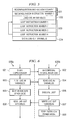
- FIGURE 2 depicts a generic instruction format for a coprocessor including a clustered VLIW architecture and a runtime reconfigurable inter-cluster bus according to one embodiment of the present invention.
- Instruction 201 issued by instruction fetch and dispatch unit 116 to clusters 109a-109n within coprocessor 102, includes a plurality of syllables 201a-201n, each syllable 201a-201n being decoded and executed by one cluster 109a-109n.
- the number of syllables 210a-201n within instruction 201 equals the number of clusters 109a-109n within coprocessor 102.
- each cluster is assumed to have an internal instruction issue width (to a respective ALU 113a-113n) of one, although wider issues are possible as in any clustered VLIW system.
- a first syllable type 202 directs the operation of traditional execution units, such as an ALU 113a-113n, contained in the cluster 109a-109n.
- a second syllable type 203 specific to the present invention, is a reconfiguration syllable directing operation of the connection box execution unit 111a-111n within the cluster 109a-109n.
- Syllables of the first type 202 is used inside the body of a loop executed on coprocessor 102, while reconfiguration syllables 203 are typically executed prior to a loop body to reconfigure the inter-cluster bus 110 (but may also be executed during a loop to dynamically reconfigure the inter-cluster bus 110).
- Syllable 202 has two parts: a first part 202a is a conventional Reduced Instruction Set Computing (RISC) type ALU instruction, and a second part 202b is an inter-cluster bus instruction directing the transmission of data over the inter-cluster bus 110.
- the first part 202a of syllable format 202 includes an operation code (opcode) identifying the computation to be performed, a destination register address (dest), a first source operand register address (source1) and a second source operand address (source2).
- opcode operation code
- the syllable 202 For each write port of a cluster register file 112a-112n (two in the exemplary embodiment) connected to the inter-cluster bus 110, the syllable 202 includes within the second part 202b one "receive" bit rcv0, rcv1 to indicate whether data should be written into the respective register file 112a-112n from the inter-cluster bus 110.
- the register file address at which the data is written is defined once with a reconfiguration instruction 203 prior to the loop execution, and is not required to be explicitly defined during the loop execution.
- the syllable 202 For each read port of a cluster register file 112a-112n (also two in the exemplary embodiment) connected to the inter-cluster bus 110, the syllable 202 includes within the second part 202b one "send" bit snd0, snd1 to indicate whether data should be read from the respective register file 112a-112n onto the inter-cluster bus 110.
- the register file address at which the data is read is defined once with a reconfiguration instruction 203 prior to the loop execution, and is not required to be explicitly defined during the loop execution.
- the send bits are not strictly required since a read may be performed at every cycle instead. However, the availability of send bits offers an opportunity to reduce power dissipation by performing read operations only when required, and are therefore preferably included.
- the format of reconfiguration syllable 203 does not include the inter-cluster bus instruction since no inter-cluster data traffic should occur during reconfiguration.
- Syllable 203 is composed of an opcode and an immediate field of reconfiguration bits encoding the reconfiguration.
- the exact format of the reconfiguration field will depend on the topology of the inter-cluster bus 110.
- FIGURE 3 depicts a suitable topology for an inter-cluster bus within a coprocessor including a clustered VLIW architecture and a runtime reconfigurable inter-cluster bus according to one embodiment of the present invention.
- inter-cluster bus 110 is composed of four machine word-size buses 301-304 arranged together with the connection boxes 111a-111n in ring fashion. Each connection box 111a-111n physically connects a number of read and write ports (not shown) of the corresponding register file 112a-112n to the buses 301-304 within the inter-cluster bus 110.
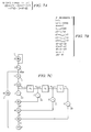
- FIGURE 4 depicts a connection box for an inter-cluster bus within a coprocessor including a clustered VLIW architecture and a runtime reconfigurable inter-cluster bus according to one embodiment of the present invention.
- the connection box 111 physically connects the inter-cluster bus 110 to the cluster register file 112, controlling connection of the read ports rd0 and rd1 and the write ports wd0 and wd1 to the buses 301-304 based on a configuration register 401.
- Configuration register 401 is set by a configuration (or reconfiguration) instruction syllable 203.
- connection box 111 sees the inter-cluster bus 110 in two parts: one connection to clusters further along the inter-cluster bus 110 on one side of the respective cluster, and one connection to clusters further along the inter-cluster bus 110 on the other side.
- Each write port wd0 and wd1 may be connected to any of buses 301-304 on either part of the inter-cluster bus 110, reading data emanating from a cluster to either side of the current cluster.
- Pass gates t01-t04 connect write port wd0 to buses 301-304 on one side, while pass gates t09-t12 connect write port wd0 to buses 301-304 on the other side.
- Pass gates t05-t08 connect write port wd1 to buses 301-304 on one side, while pass gates t13-t16 connect write port wd1 to buses 301-304 on the other side.
- each read port rd0 and rd1 can be connected to either part of the inter-cluster bus 110, writing data to a cluster situated on either side of the current cluster.
- Pass gate t19 within each of blocks 402-405 connects read port rd0 to a respective one of buses 301-304 on one side, while pass gate t21 within each of blocks 402-405 connects read port rd0 to a respective one of buses 301-304 on the other side.
- Pass gate t18 within each of blocks 402-405 connects read port rd1 to a respective one of buses 301-304 on one side, while pass gate t20 within each of blocks 402-405 connects read port rd1 to a respective one of buses 301-304 on the other side.
- connection box 111 may be configured as a pass through for the inter-cluster bus 110, meaning that a bus 301-304 from one side of the current cluster may be connected to the corresponding bus on the other side (by pass gate t17 within each of blocks 402-405). Every combination of bus connections is also possible, although the compiler should be careful to avoid illegal combinations such as two drivers writing on the same physical bus.
- connection box borrowed from the glossary of FPGA technology, is employed herein to refer to a mix of the FPGA connection box and the FPGA "switch box.”
- FIGURE 5 depicts a typical program loop executed on a coprocessor including a clustered VLIW architecture and a runtime reconfigurable inter-cluster bus according to one embodiment of the present invention.
- Each instruction depicted is equivalent to an instruction syllable 202 or 203 depicted in FIGURE 2.
- the first few instructions 501 configure the connection boxes 111.
- the exact number of instructions required to reconfigure the inter-cluster bus 110 depends on the architectural parameters, such as the number of machine word-size buses within the inter-cluster bus 110 (although that number of instructions is generally small, typically less than 4, since reconfigurable features are kept to a minimum and the instruction is very wide).
- live-in variables are loaded into registers of the various clusters by one or more instruction(s) 502.
- Live-in variables are those variables defined in the program prior to the loop and used during loop execution, communicated from processor 101 through communication mechanism 103. In the case that at most one live-in variable is required in any cluster, assuming as stated above that each cluster has an instruction issue width of one, only one instruction is required to load all live-in variables in coprocessor 102. If one cluster requires more than one live-in variable, more instructions may be required to load all necessary live-in variables.
- the loop body instructions 503 are executed.
- the instruction fetch logic of coprocessor 102 includes hardware loop support that reduces conditional branches in the code and minimizes branching overhead during execution.
- live-out variables (variables modified during loop execution and needed later in the program) are communicated to the processor by one or more instruction(s) 504 in a manner similar to the loading of live-in variables.
- FIGURE 6 is a portion of a high level flow chart illustrating execution of a program within a processing system including a processor and a coprocessor including a clustered VLIW architecture and a runtime reconfigurable inter-cluster bus according to one embodiment of the present invention.
- FIGURE 6 depicts the interaction between processor 101 and coprocessor 102, placing the program illustrated in FIGURE 5 within a larger context.
- Processor 101 and coprocessor 103 are assumed to communicate through a hardware FIFO mechanism ensuring that communication between the two components is regulated by hardware interlocks and need not be regulated by software.
- the communication might be effected through a dedicated memory space or stack, in which case software polling is required to ensure that each interlocutor is ready before communication is effected.
- processor 101 communicates to coprocessor 102 which loop needs to be executed next (step 601).
- the loop is uniquely identified and characterized by processor 101 so that coprocessor 102 knows which program address (or address range) to fetch and execute.
- the processor 101 communicates the live-in variables to the coprocessor 102 (step 603). Because a hardware FIFO mechanism is assumed, the process of communicating the live-in variables may overlap reconfiguration of the inter-cluster bus 110 and reading the live-in variables within the coprocessor 102. If the FIFO becomes full during communication of the live-in variables, the hardware mechanism will stall the processor 101; if the FIFO becomes empty before communication of the live-in variables is completed, coprocessor 102 will stall.
- processor 101 can simply wait, but is also available to perform other tasks (step 605).
- coprocessor 102 writes the live-out variables to processor 101 (step 607) and processor 101 reads the live-out variables (step 608).
- Means are provided to processor 101 to poll the status of coprocessor 102, to determine which phase of loop execution the coprocessor 102 is currently processing. This feature is useful, for example, to decide when processor 101 should exit from waiting or execution of other code (step 605), or to determine when loop execution is terminated on the coprocessor 102 if the loop has no live-out variables.
- coprocessor 102 When all live-out variables are written, coprocessor 102 typically enters a low power mode (step 609), so that processing system 100 adapts its power dissipation profile to the amount of parallelism available within the program segment being executed.
- FIGURES 7A through 7C illustrate a loop that may be scheduled for execution within a processing system including a processor and a coprocessor including a clustered VLIW architecture and a runtime reconfigurable inter-cluster bus according to one embodiment of the present invention.
- FIGURE 7A is the original C code
- FIGURE 7B is a pseudo-assembler version of the same code after two transformations have been applied
- FIGURE 7C is the Data Flow Graph (DFG) equivalent to the pseudo-assembler code in FIGURE 7B.
- DFG Data Flow Graph
- FIGURE 7B is a pseudo-assembler version of the code segment in FIGURE 7A after two transformations have been applied.
- the first transformation is load elimination, which basically promotes the use of registers (here denoted x i+1 , x i+2 and x i+3 ) to store successive values of array x. the net effect is that only one load operation is required per iteration instead of the four operations required in the original C code.
- the second transformation is predication of the loop body to enable software pipelining with kernel-only scheduling. Operand predication, as described in copending U.S. Patent Application Serial No.
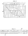
- FIGURE 8 represents a modulo reservation table used by a compiler for scheduling the loop of FIGURES 7A-7C for execution within a processing system including a processor and a coprocessor including a clustered VLIW architecture and a runtime reconfigurable inter-cluster bus according to one embodiment of the present invention.
- Modulo reservation table (MRT) 800 is employed for scheduling the DFG depicted in FIGURE 7C on a 16-cluster coprocessor 102. Because there are 16 one-issued clusters, the MRT 800 has sixteen columns, one for each cluster, while rows in the table represent time. As may be expected with an MRT, table 800 is employed to book computing resources in the clusters during scheduling of the DFG depicted in FIGURE 7C.
- Table 800 is also employed to book communication resources in the inter-cluster bus 110, with all machine word-size buses within the inter-cluster bus 110 represented by a horizontal dotted lines 801 above MRT 800 that are used to book sections of the inter-cluster bus 110 during scheduling.
- FIGURE 9 depicts two instructions generated from the final schedule obtained utilizing the modulo reservation table of FIGURE 8 to schedule the loop of FIGURES 7A-7C for execution within a processing system including a processor and a coprocessor including a clustered VLIW architecture and a runtime reconfigurable inter-cluster bus according to one embodiment of the present invention.
- the first instruction 900 is an initialization instruction 502, showing which live-in variables are written to which cluster before loop execution begins.
- the second instruction 901 is a loop body instruction 503, where the loop body in this case requires only just one instruction since the loop was successfully scheduled with an initiation interval (II) of one.
- FIGURES 1 through 9 the structure and operation of a processing system including a processor and a coprocessor including a clustered VLIW architecture and a runtime reconfigurable inter-cluster bus according to one embodiment of the present invention is described in greater detail, together with variations on the preferred embodiment.
- Cluster 109n is one of the VLIW clusters within processing system 100.
- the number of clusters within processing system 100 is a parameter of the architecture 100, but will typically be very high (e.g., sixty-four).
- all clusters 109a-109n are identical and very simple, issuing one instruction per cycle and including a small register file of registers 112 (for example, eight registers).
- All clusters 109a-109n can issue memory instructions, known as load and store instructions, which is required to be able to initialize live-in variables into, and retrieve live-out variables out of, any cluster. Support for memory instructions within each cluster also simplifies a compiler's job of scheduling instructions on the coprocessor 102. However, architecturally there need not be as many ports to memory as there are clusters (the number of memory ports is a parameter of the architecture determined for each implementation) since memory interface 108 is tasked with gathering and prioritizing all memory access requests issued by the clusters 109a-109n. If more memory access requests are made during any cycle than can be accommodated, the coprocessor 102 is stalled until all requests are satisfied.
- the inter-cluster bus 110 may be configured before the program starts or may dynamically change configuration at any cycle during program execution through specific instructions.
- the inter-cluster bus 110 is hierarchical, meaning that a cluster may be physically connected to a subset of close neighbors and indirectly connected (i.e., through two or more physical connections or hops) to the other clusters. This hierarchy is exposed in the programming model, in opposition to traditional clustered processor architectures, and is the enabling factor in effectively increasing the number of clusters that may be effectively implemented.
- inter-cluster bus 110 The precise topology and exact latency of inter-cluster bus 110 is a parameter determined for each implementation by a compromise between semiconductor area, speed and ease of programming. Unlike FPGAs and other existing reconfigurable architectures, however, connections over the inter-cluster bus should have a predictable propagation timing, one reason why, as stated above, direct physical connections between clusters are limited to neighbors. However, in the embodiment described herein, it should be noted that nothing prevents connection of any two clusters together. The compiler is tasked with the job of ensuring that the maximum distance between two connected clusters is not violated.
- this maximum distance is a function of the coprocessor clock frequency, also under control of the compiler in the preferred embodiment.
- the compiler has another option besides increasing the II, which is to keep the same II while reducing clock speed and increasing the maximum distance between two connected clusters. Both options reduce performance, but the second option possibly less than the first. Therefore, the compiler can optimize performance on a loop-by-loop basis.
- the same reasoning may be followed for power dissipation: less critical loops may be schedule with a lower clock frequency, but the resulting longer maximum distance between directly connected clusters enables more aggressive schedule and will mitigate performance loss.
- a connection over the inter-cluster bus 110 will physically connect a source register from one cluster to any of a number of destination registers in any of a number of clusters.
- the addresses of the source and destination registers are determined during a reconfiguration and remain constant until the next reconfiguration.
- no reconfiguration occurs, and data is transferred from the source register to the destination register each time the relevant "receive" and "send" bits in instruction 201 are true, without the need to specify register addresses.
- the exemplary embodiment employs pass transistors for implementation of the connection box 111, which is the most efficient implementation in terms of silicon area. Other implementations using active gates will exhibit better propagation timing at the expense of more silicon real estate.
- VLIW clusters 109a-109n and the runtime reconfigurable inter-cluster bus 110 form a general-purpose architecture
- this architecture is most efficient when closely coupled as part of a coprocessor 102 to a more traditional general-purpose processor 101, with the execution model that the coprocessor 102 executes only the parts of the program with a very high ILP, generally loops.
- the coprocessor 102 may be idled during other portions of the code to reduce power dissipation.
- the inter-cluster bus 110 is first reconfigured to form an application-specific interconnect.
- the reconfiguration bitstream is simply viewed as the first part of the program running on the coprocessor 102, and resides in the coprocessor instruction cache or program memory. If the reconfiguration bitstream is not present in the instruction cache, the initial reconfiguration operation is treated as an instruction cache miss. In this perspective, reconfiguration is treated like a particular program phase and does not require a modification of the traditional computing model or specific hardware support such as a configuration cache. Also, the very wide instruction format and the limited number of reconfigurable features for the architecture allows for an extremely fast reconfiguration. These two properties distinguish the present invention from virtually all other existing or proposed reconfigurable architectures.
- live-in variables are written to the appropriate registers within cluster 109a-109n. These registers may be memory mapped into the address space for processor 101, but such mapping would render the program running on the processing system 100 dependent on the coprocessor implementation.
- a first in, first out (FIFO) or stack mechanism 105 may be employed.
- processor-side initialization code writes the live-in variables in the FIFO or stack 105, which the runtime reconfigurable coprocessor side reads.
- a hardware FIFO 105 will allow the two initialization programs to run simultaneously, stalling either the processor 101 or the coprocessor 102 if the FIFO 105 becomes full or empty. Execution begins as soon as the configuration and initialization are complete and the first loop instruction is available.
- the processes illustrated are executed on a clustered VLIW coprocessor with an inter-cluster bus that may be configured to be application-specific at runtime, and assume that a hardware FIFO is used to transfer data between the processor and coprocessor since that is the most efficient mechanism.
- the FIFO is memory mapped for both the processor and the coprocessor.
- a software stack may alternatively be used, leading to some differences in protocol that are noted as necessary.
- FIGURE 6 illustrates execution of a data flow graph having no explicit flow control.
- the sequence of operations 600a from the processor's perspective begins with the processor informing the coprocessor which program segment to execute (step 601) by means of a pointer to memory where the program segment is located.
- the processor begins pushing live-in variables to the coprocessor (step 603).
- all live-in variables need to be pushed before the (first) coprocessor function call. Therefore, the FIFO model can be seen to be superior since a FIFO allows simultaneous instruction fetch by the coprocessor and live-in variable push by the processor.
- the compiler is then free to optionally schedule some code for execution by the processor (step 605) while reconfiguration of the inter-cluster bus is performed in the coprocessor.
- the processor may have to wait a long time here, during which there is only so much code within the current thread that can be executed. Therefore, the operating system (OS) could switch to execution of another thread that would not use the coprocessor.
- OS operating system
- the processor reads out the first live-out variable from the coprocessor (step 608), and if necessary stalls until that live-out variable value is available, which may not be before execution is entirely finished. In the stack model, the execution would have to be completed before the processor can read anything.
- the processor then reads out the remaining live-out variables.
- the coprocessor is considered finished when the last live-out variable is read from the FIFO. There is no need for signaling completion, although if the program segment (loop) has no natural live-out variable, then one must be artificially created by the compiler.
- the processor 101 then proceeds with execution of the program.
- the processor will read an exit code emitted by the coprocessor identifying exit circumstances, and might execute code to finish the current iteration and/or restart the coprocessor to finish the loop. This mechanism allows execution of a larger class of loops in the coprocessor.
- the sequence of operations 600b begins upon receiving the call instruction from the processor (step 307).
- the first instruction of the corresponding program which is a configuration instruction, is fetched unless the current configuration of the coprocessor is the desired configuration, in which case the configuration instructions are skipped.
- a left to right priority order can be defined, meaning that semantically, memory accesses in instruction 201 are executed in a left to right order.
- Such a scheme allows the compiler to fold all live-in variable read (and live-out variable write) operations in a few instructions 201. Without such a provision, the compiler would have to create one VLIW instruction 201 for each line-in and live-out variable.
- Execution of the loop program segment proper is then begun (step 606), consisting of looping through the same sequence of instructions until an exit condition is generated by one of the clusters.
- the last few instructions (as many as the maximum number of live-out variables in a single cluster, typically one, write the live-out variables to the FIFO or stack (step 607).
- the execution is finished when the last live-out variable is written, at which time the coprocessor becomes idle (step 609).
- an additional signaling is required to signify the end of execution and the integrity of the stack.
- the following description of scheduling the DFG depicted in FIGURE 7C on a 16 one-issue cluster coprocessor 102 with a 4 machine word-size inter-cluster bus 110 as depicted in FIGURES 3 and 4 is based on scheduling constraints that: the inter-cluster bus latency is zero cycles (a simplifying assumption, but one which does not compromise generality of this example); and the maximum distance between two connected clusters is three, meaning that a cluster can be directly connected to the three neighbors to one side and the three neighbors to the other side.
- the resource constrained II is one. Since there are no inter-iteration dependencies, the recurrence constrained II is zero. Those skilled in the art will recognize these terms and processes from modulo scheduling. Essentially, the conditions are met to attempt a modulo-schedule software pipelining of the loop in which a new iteration will be started every cycle.
- the columns represent clusters and the rows represent what the respective clusters do over time.
- the scheduling of one loop iteration is attempted. If successful, the scheduling of the pipeline version of the loop is derived.
- Instruction A from the DFG is scheduled on the cluster represented by column 1. Since a new iteration is started every cycle, this cluster will execute instruction A for every iteration and is therefore fully booked.
- Instruction B is scheduled on the cluster represented by column 2. Since there is a data dependence between instructions A and B (the result of A is used by B), B is scheduled one cycle later, and a portion of the inter-cluster bus is also booked as illustrated by the arrow above the first two columns. (The arrow between instructions A and B inside the MRT 800, and all other arrows between instructions inside the MRT 800, are for illustrative purposes only, depicting the DFG being scheduled, and are not part of the scheduling process.) Instruction C is then scheduled in a manner similar to instruction B, and so are the other instructions.
- inter-cluster bus has a ring topology
- the connection between instruction B and M (columns 2 and 15) is valid.
- the manner in which the two read ports of every register file connected to the inter-cluster bus may be exploited the result of instruction E is used by instruction J, and an inter-cluster bus resource is booked accordingly, but, in addition, the input to instruction E coming from instruction D is forwarded to instruction F, where that input is required a cycle later.
- the present invention provides an architecture of a runtime reconfigurable coprocessor providing performance comparable to hardwired accelerators (in both processing speed and power dissipation) on a programmable platform.
- the present invention features a large number of processing elements and can execute programs with very high instruction level parallelism, matching dedicated hardware implementations.
- the present invention has an abstract programming model for general-purpose application, and making the architecture amenable to a high level compiler target.
Applications Claiming Priority (2)
| Application Number | Priority Date | Filing Date | Title |
|---|---|---|---|
| US301372 | 2002-11-21 | ||
| US10/301,372 US8667252B2 (en) | 2002-11-21 | 2002-11-21 | Method and apparatus to adapt the clock rate of a programmable coprocessor for optimal performance and power dissipation |
Publications (2)
| Publication Number | Publication Date |
|---|---|
| EP1422618A2 true EP1422618A2 (fr) | 2004-05-26 |
| EP1422618A3 EP1422618A3 (fr) | 2005-12-07 |
Family
ID=32229899
Family Applications (1)
| Application Number | Title | Priority Date | Filing Date |
|---|---|---|---|
| EP03257332A Withdrawn EP1422618A3 (fr) | 2002-11-21 | 2003-11-20 | Coprocesseur VLIW en grappe avec un bus inter-cluster dynamiquement reconfigurable à temps d'exécution |
Country Status (2)
| Country | Link |
|---|---|
| US (1) | US8667252B2 (fr) |
| EP (1) | EP1422618A3 (fr) |
Cited By (2)
| Publication number | Priority date | Publication date | Assignee | Title |
|---|---|---|---|---|
| WO2009090541A2 (fr) * | 2008-01-16 | 2009-07-23 | Nokia Corporation | Co-processeur pour traitement de données de flux |
| KR20120019329A (ko) * | 2010-08-25 | 2012-03-06 | 삼성전자주식회사 | 프로세서, 메모리 관리 장치 및 방법 |
Families Citing this family (39)
| Publication number | Priority date | Publication date | Assignee | Title |
|---|---|---|---|---|
| US7085866B1 (en) * | 2002-02-19 | 2006-08-01 | Hobson Richard F | Hierarchical bus structure and memory access protocol for multiprocessor systems |
| US6959372B1 (en) * | 2002-02-19 | 2005-10-25 | Cogent Chipware Inc. | Processor cluster architecture and associated parallel processing methods |
| US7529368B2 (en) | 2003-04-18 | 2009-05-05 | Via Technologies, Inc. | Apparatus and method for performing transparent output feedback mode cryptographic functions |
| US8060755B2 (en) * | 2003-04-18 | 2011-11-15 | Via Technologies, Inc | Apparatus and method for providing user-generated key schedule in a microprocessor cryptographic engine |
| US7519833B2 (en) * | 2003-04-18 | 2009-04-14 | Via Technologies, Inc. | Microprocessor apparatus and method for enabling configurable data block size in a cryptographic engine |
| US7536560B2 (en) * | 2003-04-18 | 2009-05-19 | Via Technologies, Inc. | Microprocessor apparatus and method for providing configurable cryptographic key size |
| US7844053B2 (en) * | 2003-04-18 | 2010-11-30 | Ip-First, Llc | Microprocessor apparatus and method for performing block cipher cryptographic functions |
| US7529367B2 (en) * | 2003-04-18 | 2009-05-05 | Via Technologies, Inc. | Apparatus and method for performing transparent cipher feedback mode cryptographic functions |
| US7900055B2 (en) * | 2003-04-18 | 2011-03-01 | Via Technologies, Inc. | Microprocessor apparatus and method for employing configurable block cipher cryptographic algorithms |
| US7539876B2 (en) | 2003-04-18 | 2009-05-26 | Via Technologies, Inc. | Apparatus and method for generating a cryptographic key schedule in a microprocessor |
| US7532722B2 (en) * | 2003-04-18 | 2009-05-12 | Ip-First, Llc | Apparatus and method for performing transparent block cipher cryptographic functions |
| US7542566B2 (en) * | 2003-04-18 | 2009-06-02 | Ip-First, Llc | Apparatus and method for performing transparent cipher block chaining mode cryptographic functions |
| US7502943B2 (en) * | 2003-04-18 | 2009-03-10 | Via Technologies, Inc. | Microprocessor apparatus and method for providing configurable cryptographic block cipher round results |
| US7925891B2 (en) | 2003-04-18 | 2011-04-12 | Via Technologies, Inc. | Apparatus and method for employing cryptographic functions to generate a message digest |
| US7246056B1 (en) * | 2003-09-26 | 2007-07-17 | The Mathworks, Inc. | Runtime parameter mapping for system simulation |
| US7669035B2 (en) * | 2004-01-21 | 2010-02-23 | The Charles Stark Draper Laboratory, Inc. | Systems and methods for reconfigurable computing |
| EP1771792A4 (fr) * | 2004-06-08 | 2008-12-17 | Univ Rochester | Gestion dynamique du compromis entre communication et parallelisme dans des processeurs a groupes de secteurs |
| US20070074004A1 (en) * | 2005-09-28 | 2007-03-29 | Arc International (Uk) Limited | Systems and methods for selectively decoupling a parallel extended instruction pipeline |
| KR100781358B1 (ko) * | 2005-10-21 | 2007-11-30 | 삼성전자주식회사 | 데이터 처리 시스템 및 그의 데이터 처리방법 |
| JP2007122369A (ja) * | 2005-10-27 | 2007-05-17 | Canon Inc | データ処理装置及びデータ処理方法 |
| US7562206B2 (en) * | 2005-12-30 | 2009-07-14 | Intel Corporation | Multilevel scheme for dynamically and statically predicting instruction resource utilization to generate execution cluster partitions |
| US8122078B2 (en) * | 2006-10-06 | 2012-02-21 | Calos Fund, LLC | Processor with enhanced combined-arithmetic capability |
| KR101335001B1 (ko) * | 2007-11-07 | 2013-12-02 | 삼성전자주식회사 | 프로세서 및 인스트럭션 스케줄링 방법 |
| KR101390974B1 (ko) * | 2008-01-30 | 2014-05-02 | 삼성전자주식회사 | 다중 모드를 제공하는 재구성 가능한 장치 및 방법 |
| US20090198976A1 (en) * | 2008-02-06 | 2009-08-06 | Austel Vernon R | Method and structure for high-performance matrix multiplication in the presence of several architectural obstacles |
| US9792117B2 (en) | 2011-12-08 | 2017-10-17 | Oracle International Corporation | Loading values from a value vector into subregisters of a single instruction multiple data register |
| US9697174B2 (en) | 2011-12-08 | 2017-07-04 | Oracle International Corporation | Efficient hardware instructions for processing bit vectors for single instruction multiple data processors |
| US10534606B2 (en) | 2011-12-08 | 2020-01-14 | Oracle International Corporation | Run-length encoding decompression |
| GB2504772A (en) | 2012-08-10 | 2014-02-12 | Ibm | Coprocessor providing service address space for diagnostics collection |
| US11113054B2 (en) | 2013-09-10 | 2021-09-07 | Oracle International Corporation | Efficient hardware instructions for single instruction multiple data processors: fast fixed-length value compression |
| US9378232B2 (en) | 2013-09-21 | 2016-06-28 | Oracle International Corporation | Framework for numa affinitized parallel query on in-memory objects within the RDBMS |
| US20160170767A1 (en) * | 2014-12-12 | 2016-06-16 | Intel Corporation | Temporary transfer of a multithreaded ip core to single or reduced thread configuration during thread offload to co-processor |
| US10025823B2 (en) | 2015-05-29 | 2018-07-17 | Oracle International Corporation | Techniques for evaluating query predicates during in-memory table scans |
| US10067954B2 (en) | 2015-07-22 | 2018-09-04 | Oracle International Corporation | Use of dynamic dictionary encoding with an associated hash table to support many-to-many joins and aggregations |
| US10402425B2 (en) | 2016-03-18 | 2019-09-03 | Oracle International Corporation | Tuple encoding aware direct memory access engine for scratchpad enabled multi-core processors |
| US10599488B2 (en) | 2016-06-29 | 2020-03-24 | Oracle International Corporation | Multi-purpose events for notification and sequence control in multi-core processor systems |
| US10380058B2 (en) | 2016-09-06 | 2019-08-13 | Oracle International Corporation | Processor core to coprocessor interface with FIFO semantics |
| US10783102B2 (en) | 2016-10-11 | 2020-09-22 | Oracle International Corporation | Dynamically configurable high performance database-aware hash engine |
| US10176114B2 (en) | 2016-11-28 | 2019-01-08 | Oracle International Corporation | Row identification number generation in database direct memory access engine |
Citations (4)
| Publication number | Priority date | Publication date | Assignee | Title |
|---|---|---|---|---|
| EP0479390A2 (fr) * | 1990-10-05 | 1992-04-08 | Koninklijke Philips Electronics N.V. | Dispositif de traitement comprenant un circuit de mémoire et un groupe d'unités functionelles |
| WO1996008777A1 (fr) * | 1994-09-15 | 1996-03-21 | Philips Electronics N.V. | System de traitement de donnees comprenant des unites de traitement et un dispositif d'extension |
| WO1997044728A1 (fr) * | 1996-05-17 | 1997-11-27 | Advanced Micro Devices, Inc. | Processeur presentant une interconnexion de bus pouvant etre dynamiquement reconfiguree en reponse a un champ d'instructions |
| US20010014938A1 (en) * | 2000-02-04 | 2001-08-16 | Richard Bisinella | Microprocessor |
Family Cites Families (6)
| Publication number | Priority date | Publication date | Assignee | Title |
|---|---|---|---|---|
| US5574935A (en) * | 1993-12-29 | 1996-11-12 | Intel Corporation | Superscalar processor with a multi-port reorder buffer |
| US5815715A (en) * | 1995-06-05 | 1998-09-29 | Motorola, Inc. | Method for designing a product having hardware and software components and product therefor |
| DE69919059T2 (de) * | 1998-02-04 | 2005-01-27 | Texas Instruments Inc., Dallas | Datenverarbeitungssytem mit einem digitalen Signalprozessor und einem Koprozessor und Datenverarbeitungsverfahren |
| US6026479A (en) * | 1998-04-22 | 2000-02-15 | Hewlett-Packard Company | Apparatus and method for efficient switching of CPU mode between regions of high instruction level parallism and low instruction level parallism in computer programs |
| US6269437B1 (en) * | 1999-03-22 | 2001-07-31 | Agere Systems Guardian Corp. | Duplicator interconnection methods and apparatus for reducing port pressure in a clustered processor |
| US6542988B1 (en) * | 1999-10-01 | 2003-04-01 | Sun Microsystems, Inc. | Sending both a load instruction and retrieved data from a load buffer to an annex prior to forwarding the load data to register file |
-
2002
- 2002-11-21 US US10/301,372 patent/US8667252B2/en active Active
-
2003
- 2003-11-20 EP EP03257332A patent/EP1422618A3/fr not_active Withdrawn
Patent Citations (4)
| Publication number | Priority date | Publication date | Assignee | Title |
|---|---|---|---|---|
| EP0479390A2 (fr) * | 1990-10-05 | 1992-04-08 | Koninklijke Philips Electronics N.V. | Dispositif de traitement comprenant un circuit de mémoire et un groupe d'unités functionelles |
| WO1996008777A1 (fr) * | 1994-09-15 | 1996-03-21 | Philips Electronics N.V. | System de traitement de donnees comprenant des unites de traitement et un dispositif d'extension |
| WO1997044728A1 (fr) * | 1996-05-17 | 1997-11-27 | Advanced Micro Devices, Inc. | Processeur presentant une interconnexion de bus pouvant etre dynamiquement reconfiguree en reponse a un champ d'instructions |
| US20010014938A1 (en) * | 2000-02-04 | 2001-08-16 | Richard Bisinella | Microprocessor |
Cited By (6)
| Publication number | Priority date | Publication date | Assignee | Title |
|---|---|---|---|---|
| WO2009090541A2 (fr) * | 2008-01-16 | 2009-07-23 | Nokia Corporation | Co-processeur pour traitement de données de flux |
| WO2009090541A3 (fr) * | 2008-01-16 | 2009-10-15 | Nokia Corporation | Co-processeur pour traitement de données de flux |
| KR20120019329A (ko) * | 2010-08-25 | 2012-03-06 | 삼성전자주식회사 | 프로세서, 메모리 관리 장치 및 방법 |
| CN102385502A (zh) * | 2010-08-25 | 2012-03-21 | 三星电子株式会社 | 用于存储器管理的处理器、设备和方法 |
| EP2423821A3 (fr) * | 2010-08-25 | 2012-06-06 | Samsung Electronics Co., Ltd | Processeur, appareil et procédé pour l'extraction d'instructions et de configurations d'une antémémoire partagée |
| KR101710116B1 (ko) | 2010-08-25 | 2017-02-24 | 삼성전자주식회사 | 프로세서, 메모리 관리 장치 및 방법 |
Also Published As
| Publication number | Publication date |
|---|---|
| US20040103263A1 (en) | 2004-05-27 |
| US8667252B2 (en) | 2014-03-04 |
| EP1422618A3 (fr) | 2005-12-07 |
Similar Documents
| Publication | Publication Date | Title |
|---|---|---|
| US8667252B2 (en) | Method and apparatus to adapt the clock rate of a programmable coprocessor for optimal performance and power dissipation | |
| Krashinsky et al. | The vector-thread architecture | |
| Gschwind et al. | Synergistic processing in cell's multicore architecture | |
| KR100491593B1 (ko) | 데이터 처리장치 | |
| Caspi et al. | A streaming multi-threaded model | |
| TWI628594B (zh) | 用戶等級分叉及會合處理器、方法、系統及指令 | |
| US20230106990A1 (en) | Executing multiple programs simultaneously on a processor core | |
| US9275002B2 (en) | Tile-based processor architecture model for high-efficiency embedded homogeneous multicore platforms | |
| US8250507B1 (en) | Distributing computations in a parallel processing environment | |
| US6961842B2 (en) | Meta-address architecture for parallel, dynamically reconfigurable computing | |
| US20170083343A1 (en) | Out of order commit | |
| US20050268070A1 (en) | Meta-address architecture for parallel, dynamically reconfigurable computing | |
| US20070250682A1 (en) | Method and apparatus for operating a computer processor array | |
| US9213677B2 (en) | Reconfigurable processor architecture | |
| US7533382B2 (en) | Hyperprocessor | |
| US20210216454A1 (en) | Coupling wide memory interface to wide write back paths | |
| JP4784792B2 (ja) | マルチプロセッサ | |
| Krashinsky | Vector-thread architecture and implementation | |
| JP2004102988A (ja) | データ処理装置 | |
| CN115398393A (zh) | 在粗粒度可重构阵列处理器中处理多个图、上下文和程序 | |
| Zhong | Architectural and Complier Mechanisms for Accelerating Single Thread Applications on Mulitcore Processors. | |
| Examination II et al. | Hardware for Exploiting Data Level Parallelism | |
| Glökler et al. | Application-Specific Processor Architectures |
Legal Events
| Date | Code | Title | Description |
|---|---|---|---|
| PUAI | Public reference made under article 153(3) epc to a published international application that has entered the european phase |
Free format text: ORIGINAL CODE: 0009012 |
|
| AK | Designated contracting states |
Kind code of ref document: A2 Designated state(s): AT BE BG CH CY CZ DE DK EE ES FI FR GB GR HU IE IT LI LU MC NL PT RO SE SI SK TR |
|
| AX | Request for extension of the european patent |
Extension state: AL LT LV MK |
|
| PUAL | Search report despatched |
Free format text: ORIGINAL CODE: 0009013 |
|
| AK | Designated contracting states |
Kind code of ref document: A3 Designated state(s): AT BE BG CH CY CZ DE DK EE ES FI FR GB GR HU IE IT LI LU MC NL PT RO SE SI SK TR |
|
| AX | Request for extension of the european patent |
Extension state: AL LT LV MK |
|
| 17P | Request for examination filed |
Effective date: 20060526 |
|
| AKX | Designation fees paid | ||
| RBV | Designated contracting states (corrected) |
Designated state(s): DE FR GB IT |
|
| REG | Reference to a national code |
Ref country code: DE Ref legal event code: 8566 |
|
| STAA | Information on the status of an ep patent application or granted ep patent |
Free format text: STATUS: THE APPLICATION HAS BEEN WITHDRAWN |
|
| 18W | Application withdrawn |
Effective date: 20061006 |