EP1422541A2 - Process for producing three-dimensional polyimide optical waveguide - Google Patents
Process for producing three-dimensional polyimide optical waveguide Download PDFInfo
- Publication number
- EP1422541A2 EP1422541A2 EP03026967A EP03026967A EP1422541A2 EP 1422541 A2 EP1422541 A2 EP 1422541A2 EP 03026967 A EP03026967 A EP 03026967A EP 03026967 A EP03026967 A EP 03026967A EP 1422541 A2 EP1422541 A2 EP 1422541A2
- Authority
- EP
- European Patent Office
- Prior art keywords
- polyamic acid
- process according
- dihydropyridine
- film
- laser beam
- Prior art date
- Legal status (The legal status is an assumption and is not a legal conclusion. Google has not performed a legal analysis and makes no representation as to the accuracy of the status listed.)
- Granted
Links
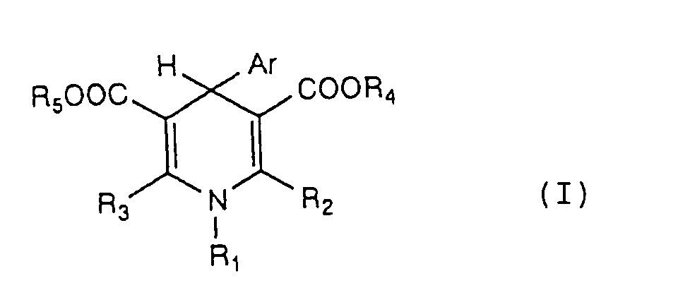
- 0 *C1=C(*)N(*)C(*)=C(*)C1[Al] Chemical compound *C1=C(*)N(*)C(*)=C(*)C1[Al] 0.000 description 1
Images

Classifications
-
- G—PHYSICS
- G02—OPTICS
- G02B—OPTICAL ELEMENTS, SYSTEMS OR APPARATUS
- G02B6/00—Light guides; Structural details of arrangements comprising light guides and other optical elements, e.g. couplings
- G02B6/10—Light guides; Structural details of arrangements comprising light guides and other optical elements, e.g. couplings of the optical waveguide type
- G02B6/12—Light guides; Structural details of arrangements comprising light guides and other optical elements, e.g. couplings of the optical waveguide type of the integrated circuit kind
- G02B6/13—Integrated optical circuits characterised by the manufacturing method
-
- C—CHEMISTRY; METALLURGY
- C08—ORGANIC MACROMOLECULAR COMPOUNDS; THEIR PREPARATION OR CHEMICAL WORKING-UP; COMPOSITIONS BASED THEREON
- C08G—MACROMOLECULAR COMPOUNDS OBTAINED OTHERWISE THAN BY REACTIONS ONLY INVOLVING UNSATURATED CARBON-TO-CARBON BONDS
- C08G73/00—Macromolecular compounds obtained by reactions forming a linkage containing nitrogen with or without oxygen or carbon in the main chain of the macromolecule, not provided for in groups C08G12/00 - C08G71/00
- C08G73/06—Polycondensates having nitrogen-containing heterocyclic rings in the main chain of the macromolecule
- C08G73/10—Polyimides; Polyester-imides; Polyamide-imides; Polyamide acids or similar polyimide precursors
-
- G—PHYSICS
- G02—OPTICS
- G02B—OPTICAL ELEMENTS, SYSTEMS OR APPARATUS
- G02B1/00—Optical elements characterised by the material of which they are made; Optical coatings for optical elements
- G02B1/04—Optical elements characterised by the material of which they are made; Optical coatings for optical elements made of organic materials, e.g. plastics
- G02B1/045—Light guides
-
- G—PHYSICS
- G02—OPTICS
- G02B—OPTICAL ELEMENTS, SYSTEMS OR APPARATUS
- G02B1/00—Optical elements characterised by the material of which they are made; Optical coatings for optical elements
- G02B1/04—Optical elements characterised by the material of which they are made; Optical coatings for optical elements made of organic materials, e.g. plastics
- G02B1/045—Light guides
- G02B1/046—Light guides characterised by the core material
-
- G—PHYSICS
- G02—OPTICS
- G02B—OPTICAL ELEMENTS, SYSTEMS OR APPARATUS
- G02B6/00—Light guides; Structural details of arrangements comprising light guides and other optical elements, e.g. couplings
- G02B6/10—Light guides; Structural details of arrangements comprising light guides and other optical elements, e.g. couplings of the optical waveguide type
- G02B6/12—Light guides; Structural details of arrangements comprising light guides and other optical elements, e.g. couplings of the optical waveguide type of the integrated circuit kind
- G02B6/12002—Three-dimensional structures
-
- G—PHYSICS
- G02—OPTICS
- G02B—OPTICAL ELEMENTS, SYSTEMS OR APPARATUS
- G02B6/00—Light guides; Structural details of arrangements comprising light guides and other optical elements, e.g. couplings
- G02B6/10—Light guides; Structural details of arrangements comprising light guides and other optical elements, e.g. couplings of the optical waveguide type
- G02B6/12—Light guides; Structural details of arrangements comprising light guides and other optical elements, e.g. couplings of the optical waveguide type of the integrated circuit kind
- G02B6/122—Basic optical elements, e.g. light-guiding paths
- G02B6/1221—Basic optical elements, e.g. light-guiding paths made from organic materials
Definitions
- the present inventors have made extensive investigations. As a result, it was discovered that by irradiating an inside portion of a polyamic acid film having incorporated therein a photosensitive agent, with such a low power.laser beam that is unreactive to the polyamic acid, but reactive only to the photosensitive agent, while relatively moving a light convergence point thereof, followed by imidation of the polyamic acid, an effective difference in the refraction index can be obtained between the irradiated area and the non-irradiated area, thus being able to easily form the three-dimensional polyimide optical waveguide.
- the invention has been accomplished.
- the average output or irradiation energy of the pulse laser is not particularly limited, and it can be appropriately selected depending on the intended size of the core, the required difference in the refraction index between the irradiated area (core) and the non-irradiated area (clad), etc. Usually, it is within the range of 1 to 500 mW, preferably within the range of 5 to 300 mW, and most preferably within the range of 10 to 100 mW. As described above, according to the invention, the irradiation energy of a pulse laser beam may be low.
- the shape of the core precursor including the diameter, width and longitudinal shape thereof, and the cross sectional shape thereof are not particularly limited.
- the diameter or width of the core precursor is suitably ranges from about 0.1 to about 1,000 ⁇ m, preferably from about 0.1 to about 100 ⁇ m, and more preferably from about 0.5 to about 30 ⁇ m.
- the longitudinal shape of the core precursor may be either a linear shape or a crooked or inflected shape. Further, it may be a combined shape of a linear shape and a crooked or inflected shape.
- the longitudinal length of the core precursor is also not particularly limited.
- the cross sectional shape of the core precursor may be, for example, substantially circular or substantially polygonal (for example, substantially quadrilateral).
Landscapes
- Physics & Mathematics (AREA)
- General Physics & Mathematics (AREA)
- Optics & Photonics (AREA)
- Engineering & Computer Science (AREA)
- Microelectronics & Electronic Packaging (AREA)
- Chemical & Material Sciences (AREA)
- Health & Medical Sciences (AREA)
- Chemical Kinetics & Catalysis (AREA)
- Medicinal Chemistry (AREA)
- Polymers & Plastics (AREA)
- Organic Chemistry (AREA)
- Optical Integrated Circuits (AREA)
- Compositions Of Macromolecular Compounds (AREA)
- Macromolecular Compounds Obtained By Forming Nitrogen-Containing Linkages In General (AREA)
Abstract

Description

Claims (12)
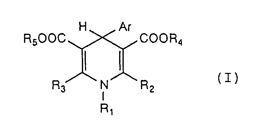
- A process for producing a three-dimensional polyimide optical waveguide, which comprises:(I) irradiating a polyamic acid film with a laser beam while converging the laser beam at an inside portion of the film and relatively moving the light convergence point, the polyamic acid film containing:wherein Ar represents an aromatic group having a nitro group at an ortho-position with respect to the bonding position to the 1,4-dihydropyridine ring; R1 represents a hydrogen atom or an alkyl group having 1 to 3 carbon atoms; and R2, R3, R4 and R5 each independently represents a hydrogen atom or an alkyl group having 1 or 2 carbon atoms, and then,(a) a polyamic acid obtained from a tetracarboxylic dianhydride and a diamine; and(b) per 100 parts of the polyamic acid, from 0.5 part by weight to less than 10 parts by weight of a 1,4-dihydropyridine derivative represented by formula (I):
 (II) heating the polyamic acid film to imidize the polyamic acid, thereby obtaining an optical waveguide having a continuous core region where the refraction index has been changed, in the thus formed polyimide film.
 - The process according to claim 1, wherein the tetracarboxylic dianhydride contains a fluorine atom.
- The process according to claim 1, wherein the diamine contains a fluorine atom.
- The process according to claim 1, wherein the 1,4-dihydropyridine derivative represented by formula (I) is selected from the group consisting of 1-ethyl-3,5-dimethoxycarbonyl-4-(2-nitrophenyl)-1,4-dihydropyridine, 1-methyl-3,5-dimethoxycarbonyl-4-(2-nitrophenyl)-1,4-dihydropyridine, 1-propyl-3,5-dimethoxycarbonyl-4-(2-nitrophenyl)-1,4-dihydropyridine and 1-propyl-3,5-diethoxycarbonyl-4-(2-nitrophenyl)-1,4-dihydropyridine.
- The process according to claim 4, wherein the 1,4-dihydropyridine derivative represented by formula (I) comprises 1-ethyl-3,5-dimethoxycarbonyl-4-(2-nitrophenyl)-1,4-dihydropyridine.
- The process according to claim 1, wherein the laser beam is a pulse laser having a pulse width of 10-15 to 10-12 second.
- The process according to claim 6, wherein the pulse width is 10 x 10-15 to 500 x 10-15 second.
- The process according to claim 7, wherein the pulse width is about 50 x 10-15 to about 300 x 10-15 second.
- The process according to claim 6, wherein the pulse laser has a repeating frequency of from 1 Hz to 80 MHz.
- The process according to claim 9, wherein the repeating frequency is from 10 Hz to 500 kHz.
- The process according to claim 6, wherein the irradiation of the pulse laser is carried out at an irradiation energy of from 1 to 500 mW.
- The process according to claim 11, wherein the irradiation energy of the pulse laser is from 10 to 100 mW.
Applications Claiming Priority (2)
| Application Number | Priority Date | Filing Date | Title |
|---|---|---|---|
| JP2002341565A JP3987787B2 (en) | 2002-11-25 | 2002-11-25 | Manufacturing method of three-dimensional polyimide optical waveguide |
| JP2002341565 | 2002-11-25 |
Publications (3)
| Publication Number | Publication Date |
|---|---|
| EP1422541A2 true EP1422541A2 (en) | 2004-05-26 |
| EP1422541A3 EP1422541A3 (en) | 2004-07-14 |
| EP1422541B1 EP1422541B1 (en) | 2007-09-05 |
Family
ID=32212167
Family Applications (1)
| Application Number | Title | Priority Date | Filing Date |
|---|---|---|---|
| EP03026967A Expired - Lifetime EP1422541B1 (en) | 2002-11-25 | 2003-11-25 | Process for producing three-dimensional polyimide optical waveguide |
Country Status (6)
| Country | Link |
|---|---|
| US (1) | US7085469B2 (en) |
| EP (1) | EP1422541B1 (en) |
| JP (1) | JP3987787B2 (en) |
| KR (1) | KR100798218B1 (en) |
| CN (1) | CN1300611C (en) |
| DE (1) | DE60316096T2 (en) |
Cited By (2)
| Publication number | Priority date | Publication date | Assignee | Title |
|---|---|---|---|---|
| FR2871582A1 (en) * | 2004-06-11 | 2005-12-16 | Univ Louis Pasteur Etablisseme | METHOD FOR MANUFACTURING AN OPTICAL CIRCUIT OPTICAL BLOCK INTEGRATED BY LOCALIZED PHOTOPOLYMERIZATION OF AN ORGANIC MATRIX BY TWO-PHOTON ABSORPTION AND OPTICAL BLOCK THUS OBTAINED |
| WO2012143070A1 (en) * | 2011-04-16 | 2012-10-26 | Technische Universität Berlin | Method for producing an optical fibre in a polymer |
Families Citing this family (13)
| Publication number | Priority date | Publication date | Assignee | Title |
|---|---|---|---|---|
| US7037637B2 (en) * | 2002-07-17 | 2006-05-02 | Nitto Denko Corporation | Photosensitive polyimide resin precursor composition, optical polyimide obtained from the composition, optical waveguide using the polyimide, and process for producing the optical waveguide |
| WO2007046833A2 (en) * | 2004-12-20 | 2007-04-26 | Imra America, Inc. | Pulsed laser source with adjustable grating compressor |
| KR100705758B1 (en) * | 2005-04-19 | 2007-04-10 | 한국과학기술원 | Flexible film optical waveguide using organic-inorganic hybrid material and method for manufacturing same |
| US7789910B2 (en) * | 2006-06-28 | 2010-09-07 | Bausch & Lomb Incorporated | Optical material and method for modifying the refractive index |
| US20080001320A1 (en) | 2006-06-28 | 2008-01-03 | Knox Wayne H | Optical Material and Method for Modifying the Refractive Index |
| WO2009070438A1 (en) * | 2007-11-30 | 2009-06-04 | Bausch & Lomb Incorporated | Optical material and method for modifying the refractive index |
| US9060847B2 (en) * | 2008-05-19 | 2015-06-23 | University Of Rochester | Optical hydrogel material with photosensitizer and method for modifying the refractive index |
| TWI394992B (en) * | 2008-12-02 | 2013-05-01 | Univ Nat Central | Fabrication device and method for producing high molecular optical waveguide element |
| WO2011089592A1 (en) * | 2010-01-20 | 2011-07-28 | Moshe Finarov | A method of laser processing |
| US9144491B2 (en) | 2011-06-02 | 2015-09-29 | University Of Rochester | Method for modifying the refractive index of an optical material |
| JP6038787B2 (en) * | 2011-06-27 | 2016-12-07 | 学校法人慶應義塾 | Manufacturing method of optical waveguide |
| WO2015060822A1 (en) * | 2013-10-22 | 2015-04-30 | Empire Technology Development Llc | Thermally printed optic circuits |
| CN119610708B (en) * | 2024-12-09 | 2025-10-17 | 广东工业大学 | Processing method of three-dimensional hot cloak |
Family Cites Families (14)
| Publication number | Priority date | Publication date | Assignee | Title |
|---|---|---|---|---|
| WO1992000185A1 (en) | 1990-06-22 | 1992-01-09 | Martin Russell Harris | Optical waveguides |
| US5851736A (en) * | 1991-03-05 | 1998-12-22 | Nitto Denko Corporation | Heat-resistant photoresist composition, photosensitive substrate, and process for forming heat-resistant positive or negative pattern |
| JPH06337320A (en) | 1993-05-27 | 1994-12-06 | Agency Of Ind Science & Technol | Process and apparatus for production of optical waveguide |
| EP1315006A1 (en) | 1994-06-22 | 2003-05-28 | Fujitsu Limited | Method of producing optical waveguide system, optical device and optical coupler employing the same, optical network and optical circuit board |
| SG55276A1 (en) * | 1996-02-13 | 1998-12-21 | Nitto Denko Corp | Circuit substrate circuit-formed suspension substrate and production method thereof |
| SG52916A1 (en) * | 1996-02-13 | 1998-09-28 | Nitto Denko Corp | Circuit substrate circuit-formed suspension substrate and production method thereof |
| JP2000112126A (en) * | 1998-10-01 | 2000-04-21 | Nitto Denko Corp | Negative photoresist composition |
| US6177225B1 (en) * | 1998-10-01 | 2001-01-23 | Arch Specialty Chemicals, Inc. | Photosensitive resin compositions |
| US20010021293A1 (en) * | 2000-02-22 | 2001-09-13 | Hikaru Kouta | Method for modifying refractive index in optical wave-guide device |
| JP4965052B2 (en) * | 2000-06-15 | 2012-07-04 | スリーエム イノベイティブ プロパティズ カンパニー | Processing method of three-dimensional optical element |
| JP2002014246A (en) | 2000-06-27 | 2002-01-18 | Matsushita Electric Works Ltd | Optical waveguide and method for manufacturing the same |
| JP2002148804A (en) | 2000-11-08 | 2002-05-22 | Nitto Denko Corp | Photosensitive resin composition and circuit board |
| JP4799764B2 (en) * | 2001-05-31 | 2011-10-26 | 日東電工株式会社 | Photosensitive polyimide precursor composition for optical waveguide, photosensitive polyimide composition for optical waveguide, and optical waveguide using the same |
| US7037637B2 (en) * | 2002-07-17 | 2006-05-02 | Nitto Denko Corporation | Photosensitive polyimide resin precursor composition, optical polyimide obtained from the composition, optical waveguide using the polyimide, and process for producing the optical waveguide |
-
2002
- 2002-11-25 JP JP2002341565A patent/JP3987787B2/en not_active Expired - Fee Related
-
2003
- 2003-11-05 US US10/700,635 patent/US7085469B2/en not_active Expired - Fee Related
- 2003-11-24 KR KR1020030083490A patent/KR100798218B1/en not_active Expired - Fee Related
- 2003-11-25 EP EP03026967A patent/EP1422541B1/en not_active Expired - Lifetime
- 2003-11-25 CN CNB2003101181932A patent/CN1300611C/en not_active Expired - Fee Related
- 2003-11-25 DE DE60316096T patent/DE60316096T2/en not_active Expired - Fee Related
Cited By (3)
| Publication number | Priority date | Publication date | Assignee | Title |
|---|---|---|---|---|
| FR2871582A1 (en) * | 2004-06-11 | 2005-12-16 | Univ Louis Pasteur Etablisseme | METHOD FOR MANUFACTURING AN OPTICAL CIRCUIT OPTICAL BLOCK INTEGRATED BY LOCALIZED PHOTOPOLYMERIZATION OF AN ORGANIC MATRIX BY TWO-PHOTON ABSORPTION AND OPTICAL BLOCK THUS OBTAINED |
| WO2006003313A1 (en) * | 2004-06-11 | 2006-01-12 | Universite Louis Pasteur, U.L.P. | Method for making an optical block with an integrated optical circuit by spot photopolymerisation of an organic matrix via two-photon absorption and optical block thus obtained |
| WO2012143070A1 (en) * | 2011-04-16 | 2012-10-26 | Technische Universität Berlin | Method for producing an optical fibre in a polymer |
Also Published As
| Publication number | Publication date |
|---|---|
| US20040131324A1 (en) | 2004-07-08 |
| EP1422541A3 (en) | 2004-07-14 |
| CN1503016A (en) | 2004-06-09 |
| KR100798218B1 (en) | 2008-01-24 |
| DE60316096D1 (en) | 2007-10-18 |
| DE60316096T2 (en) | 2008-01-03 |
| US7085469B2 (en) | 2006-08-01 |
| JP3987787B2 (en) | 2007-10-10 |
| CN1300611C (en) | 2007-02-14 |
| JP2004177529A (en) | 2004-06-24 |
| EP1422541B1 (en) | 2007-09-05 |
| KR20040045371A (en) | 2004-06-01 |
Similar Documents
| Publication | Publication Date | Title |
|---|---|---|
| EP1422541B1 (en) | Process for producing three-dimensional polyimide optical waveguide | |
| US7037637B2 (en) | Photosensitive polyimide resin precursor composition, optical polyimide obtained from the composition, optical waveguide using the polyimide, and process for producing the optical waveguide | |
| EP1424577B1 (en) | Process for producing polyimide optical waveguide | |
| JP4799764B2 (en) | Photosensitive polyimide precursor composition for optical waveguide, photosensitive polyimide composition for optical waveguide, and optical waveguide using the same | |
| JP2004309683A (en) | Optical waveguides and gratings, lenses, photonic crystals, and methods for producing them. | |
| JP3841288B2 (en) | Photosensitive polyimide resin precursor composition, optical polyimide and optical waveguide obtained therefrom | |
| US7236675B2 (en) | Process for producing optical waveguide | |
| JP4010011B2 (en) | Optical waveguide structure | |
| KR20040068470A (en) | Process of manufacturing optical waveguide and connection structure of optical device | |
| JP4071175B2 (en) | Method for producing polyimide optical element | |
| JP2005148124A (en) | Photosensitive polyamic acid composition, optical polyimide resin and optical waveguide obtained therefrom | |
| JP3302157B2 (en) | Method for manufacturing fluorinated polyimide optical waveguide | |
| JP4676910B2 (en) | Optical component, optical waveguide, and manufacturing method thereof | |
| WO2005101074A1 (en) | Optical waveguide | |
| JP2007033776A (en) | Manufacturing method of laminated optical waveguide | |
| JP2005017429A (en) | Manufacturing method of optical waveguide | |
| JPH07209536A (en) | Polyimide optical waveguide manufacturing apparatus and polyimide optical waveguide manufacturing method | |
| JP2007219560A (en) | Optical waveguide structure | |
| JPWO1997047998A1 (en) | Optical Waveguides and Optical Devices |
Legal Events
| Date | Code | Title | Description |
|---|---|---|---|
| PUAI | Public reference made under article 153(3) epc to a published international application that has entered the european phase |
Free format text: ORIGINAL CODE: 0009012 |
|
| AK | Designated contracting states |
Kind code of ref document: A2 Designated state(s): AT BE BG CH CY CZ DE DK EE ES FI FR GB GR HU IE IT LI LU MC NL PT RO SE SI SK TR |
|
| AX | Request for extension of the european patent |
Extension state: AL LT LV MK |
|
| PUAL | Search report despatched |
Free format text: ORIGINAL CODE: 0009013 |
|
| AK | Designated contracting states |
Kind code of ref document: A3 Designated state(s): AT BE BG CH CY CZ DE DK EE ES FI FR GB GR HU IE IT LI LU MC NL PT RO SE SI SK TR |
|
| AX | Request for extension of the european patent |
Extension state: AL LT LV MK |
|
| 17P | Request for examination filed |
Effective date: 20040924 |
|
| AKX | Designation fees paid |
Designated state(s): DE FR GB |
|
| GRAP | Despatch of communication of intention to grant a patent |
Free format text: ORIGINAL CODE: EPIDOSNIGR1 |
|
| RIC1 | Information provided on ipc code assigned before grant |
Ipc: C08L 79/00 20060101ALI20070301BHEP Ipc: G02B 1/04 20060101ALI20070301BHEP Ipc: G02B 6/138 20060101AFI20070301BHEP |
|
| GRAS | Grant fee paid |
Free format text: ORIGINAL CODE: EPIDOSNIGR3 |
|
| GRAA | (expected) grant |
Free format text: ORIGINAL CODE: 0009210 |
|
| AK | Designated contracting states |
Kind code of ref document: B1 Designated state(s): DE FR GB |
|
| REG | Reference to a national code |
Ref country code: GB Ref legal event code: FG4D |
|
| REF | Corresponds to: |
Ref document number: 60316096 Country of ref document: DE Date of ref document: 20071018 Kind code of ref document: P |
|
| ET | Fr: translation filed | ||
| PGFP | Annual fee paid to national office [announced via postgrant information from national office to epo] |
Ref country code: FR Payment date: 20071126 Year of fee payment: 5 |
|
| PLBE | No opposition filed within time limit |
Free format text: ORIGINAL CODE: 0009261 |
|
| STAA | Information on the status of an ep patent application or granted ep patent |
Free format text: STATUS: NO OPPOSITION FILED WITHIN TIME LIMIT |
|
| 26N | No opposition filed |
Effective date: 20080606 |
|
| PGFP | Annual fee paid to national office [announced via postgrant information from national office to epo] |
Ref country code: DE Payment date: 20081120 Year of fee payment: 6 |
|
| PGFP | Annual fee paid to national office [announced via postgrant information from national office to epo] |
Ref country code: GB Payment date: 20081119 Year of fee payment: 6 |
|
| REG | Reference to a national code |
Ref country code: FR Ref legal event code: ST Effective date: 20090731 |
|
| GBPC | Gb: european patent ceased through non-payment of renewal fee |
Effective date: 20091125 |
|
| PG25 | Lapsed in a contracting state [announced via postgrant information from national office to epo] |
Ref country code: DE Free format text: LAPSE BECAUSE OF NON-PAYMENT OF DUE FEES Effective date: 20100601 |
|
| PG25 | Lapsed in a contracting state [announced via postgrant information from national office to epo] |
Ref country code: GB Free format text: LAPSE BECAUSE OF NON-PAYMENT OF DUE FEES Effective date: 20091125 |
|
| PG25 | Lapsed in a contracting state [announced via postgrant information from national office to epo] |
Ref country code: FR Free format text: LAPSE BECAUSE OF NON-PAYMENT OF DUE FEES Effective date: 20081130 |