EP1420385A2 - Liquid crystal display and driving method thereof - Google Patents
Liquid crystal display and driving method thereof Download PDFInfo
- Publication number
- EP1420385A2 EP1420385A2 EP03026083A EP03026083A EP1420385A2 EP 1420385 A2 EP1420385 A2 EP 1420385A2 EP 03026083 A EP03026083 A EP 03026083A EP 03026083 A EP03026083 A EP 03026083A EP 1420385 A2 EP1420385 A2 EP 1420385A2
- Authority
- EP
- European Patent Office
- Prior art keywords
- image data
- gamma
- luminance
- data
- liquid crystal
- Prior art date
- Legal status (The legal status is an assumption and is not a legal conclusion. Google has not performed a legal analysis and makes no representation as to the accuracy of the status listed.)
- Granted
Links
Images




Classifications
-
- G—PHYSICS
- G02—OPTICS
- G02F—OPTICAL DEVICES OR ARRANGEMENTS FOR THE CONTROL OF LIGHT BY MODIFICATION OF THE OPTICAL PROPERTIES OF THE MEDIA OF THE ELEMENTS INVOLVED THEREIN; NON-LINEAR OPTICS; FREQUENCY-CHANGING OF LIGHT; OPTICAL LOGIC ELEMENTS; OPTICAL ANALOGUE/DIGITAL CONVERTERS
- G02F1/00—Devices or arrangements for the control of the intensity, colour, phase, polarisation or direction of light arriving from an independent light source, e.g. switching, gating or modulating; Non-linear optics
- G02F1/01—Devices or arrangements for the control of the intensity, colour, phase, polarisation or direction of light arriving from an independent light source, e.g. switching, gating or modulating; Non-linear optics for the control of the intensity, phase, polarisation or colour
- G02F1/13—Devices or arrangements for the control of the intensity, colour, phase, polarisation or direction of light arriving from an independent light source, e.g. switching, gating or modulating; Non-linear optics for the control of the intensity, phase, polarisation or colour based on liquid crystals, e.g. single liquid crystal display cells
- G02F1/133—Constructional arrangements; Operation of liquid crystal cells; Circuit arrangements
-
- G—PHYSICS
- G09—EDUCATION; CRYPTOGRAPHY; DISPLAY; ADVERTISING; SEALS
- G09G—ARRANGEMENTS OR CIRCUITS FOR CONTROL OF INDICATING DEVICES USING STATIC MEANS TO PRESENT VARIABLE INFORMATION
- G09G3/00—Control arrangements or circuits, of interest only in connection with visual indicators other than cathode-ray tubes
- G09G3/20—Control arrangements or circuits, of interest only in connection with visual indicators other than cathode-ray tubes for presentation of an assembly of a number of characters, e.g. a page, by composing the assembly by combination of individual elements arranged in a matrix no fixed position being assigned to or needed to be assigned to the individual characters or partial characters
- G09G3/2092—Details of a display terminals using a flat panel, the details relating to the control arrangement of the display terminal and to the interfaces thereto
-
- G—PHYSICS
- G09—EDUCATION; CRYPTOGRAPHY; DISPLAY; ADVERTISING; SEALS
- G09G—ARRANGEMENTS OR CIRCUITS FOR CONTROL OF INDICATING DEVICES USING STATIC MEANS TO PRESENT VARIABLE INFORMATION
- G09G3/00—Control arrangements or circuits, of interest only in connection with visual indicators other than cathode-ray tubes
- G09G3/20—Control arrangements or circuits, of interest only in connection with visual indicators other than cathode-ray tubes for presentation of an assembly of a number of characters, e.g. a page, by composing the assembly by combination of individual elements arranged in a matrix no fixed position being assigned to or needed to be assigned to the individual characters or partial characters
- G09G3/34—Control arrangements or circuits, of interest only in connection with visual indicators other than cathode-ray tubes for presentation of an assembly of a number of characters, e.g. a page, by composing the assembly by combination of individual elements arranged in a matrix no fixed position being assigned to or needed to be assigned to the individual characters or partial characters by control of light from an independent source
- G09G3/36—Control arrangements or circuits, of interest only in connection with visual indicators other than cathode-ray tubes for presentation of an assembly of a number of characters, e.g. a page, by composing the assembly by combination of individual elements arranged in a matrix no fixed position being assigned to or needed to be assigned to the individual characters or partial characters by control of light from an independent source using liquid crystals
- G09G3/3611—Control of matrices with row and column drivers
-
- G—PHYSICS
- G09—EDUCATION; CRYPTOGRAPHY; DISPLAY; ADVERTISING; SEALS
- G09G—ARRANGEMENTS OR CIRCUITS FOR CONTROL OF INDICATING DEVICES USING STATIC MEANS TO PRESENT VARIABLE INFORMATION
- G09G2320/00—Control of display operating conditions
- G09G2320/02—Improving the quality of display appearance
- G09G2320/0271—Adjustment of the gradation levels within the range of the gradation scale, e.g. by redistribution or clipping
- G09G2320/0276—Adjustment of the gradation levels within the range of the gradation scale, e.g. by redistribution or clipping for the purpose of adaptation to the characteristics of a display device, i.e. gamma correction
-
- G—PHYSICS
- G09—EDUCATION; CRYPTOGRAPHY; DISPLAY; ADVERTISING; SEALS
- G09G—ARRANGEMENTS OR CIRCUITS FOR CONTROL OF INDICATING DEVICES USING STATIC MEANS TO PRESENT VARIABLE INFORMATION
- G09G2320/00—Control of display operating conditions
- G09G2320/06—Adjustment of display parameters
- G09G2320/0626—Adjustment of display parameters for control of overall brightness
-
- G—PHYSICS
- G09—EDUCATION; CRYPTOGRAPHY; DISPLAY; ADVERTISING; SEALS
- G09G—ARRANGEMENTS OR CIRCUITS FOR CONTROL OF INDICATING DEVICES USING STATIC MEANS TO PRESENT VARIABLE INFORMATION
- G09G3/00—Control arrangements or circuits, of interest only in connection with visual indicators other than cathode-ray tubes
- G09G3/20—Control arrangements or circuits, of interest only in connection with visual indicators other than cathode-ray tubes for presentation of an assembly of a number of characters, e.g. a page, by composing the assembly by combination of individual elements arranged in a matrix no fixed position being assigned to or needed to be assigned to the individual characters or partial characters
- G09G3/34—Control arrangements or circuits, of interest only in connection with visual indicators other than cathode-ray tubes for presentation of an assembly of a number of characters, e.g. a page, by composing the assembly by combination of individual elements arranged in a matrix no fixed position being assigned to or needed to be assigned to the individual characters or partial characters by control of light from an independent source
- G09G3/3406—Control of illumination source
Definitions
- the present invention relates to a liquid crystal display and a driving method thereof.
- a flat panel display such as a liquid crystal display (LCD) has been developed instead of the cathode ray tube, and applied for practical use in the field of computers, and televisions.
- LCD liquid crystal display
- the LCD has a panel with a matrix-typed pixel pattern, and a counter panel facing the former panel.
- a liquid crystal material bearing a dielectric anisotropy is injected between the two panels. The light transmission through the panels is controlled through varying the strength of the electric fields applied to both ends of the two panels, thereby displaying the desired images.
- the display device usually represents original images on the screen by way of the RGB color space intrinsic thereto. That is, when the color space is expressed by way of a plurality of gray levels, gamma correction is made by way of a luminance curve corresponding to each gray level, that is, by way of a gamma curve. A color correction is additionally made, thereby recovering the original images.
- the RGB color space is mostly device-dependent, the designer of the display device as well as the user thereof should consider the image profile intrinsic to the device when the original images are represented. This is a considerable burden to them. As the kind and the characteristic of the display device are diversified in various manners, it is needed to make a definition of a standard color space for the display device.
- a need is made to realize such a sRGB color space with the LCD.
- the display luminance level with respect to the maximum input gray level should be established to be 80cd/m 2 .
- the gamma curve expressing the luminance characteristic of the input gray level should agree to the gamma 2.2 curve.
- the display model offset with respect to the RGB colors should be established to be zero.
- the liquid crystal display includes a signal controller having a luminance controller receiving image data from an external graphic source and controlling the luminance of the image data such that the luminance at the gray expressed by a specific data value of the image data is established to be 80cd/m 2 , and a gamma converter outputting image data each having a gamma characteristic adapted to the gamma 2.2 curve.
- the liquid crystal display further includes a data driver receiving the image data from the signal controller and selecting and outputting gray voltages corresponding to the image data, and an inverter controlling a lamp such that the lamp emits light with a luminance of 80cd/m 2 or more.
- the luminance of a backlight is determined to be a specific value larger than 80cd/m 2 , and the luminance of the input image data is controlled such that the luminance thereof at the specific data value is established to be 80cd/m 2 .
- the gamma characteristic of the image data RGB is converted to be adapted to the gamma 2.2 curve required for the sRGB color space. In this way, the sRGB mode is realized with the liquid crystal display, and the display quality of the liquid crystal display can be improved.
- Fig. 1 is a block diagram of an LCD according to an embodiment of the present invention.
- an LCD includes a liquid crystal panel assembly 10, a gate driver 20, a data driver 30, a signal controller 40, a voltage generator 50, a lamp 60, and an inverter 70.
- the liquid crystal panel assembly 10 includes a plurality of gate lines (not shown) extending in a transverse direction and transmitting gate voltages, a plurality of data lines (not shown) extending in a longitudinal direction and transmitting data voltages, and a plurality of pixels (not shown) connected to the gate lines and the data lines and arranged in a matrix.
- Each pixel includes a liquid crystal capacitor (not shown) and a switching element such as a thin film transistor (TFT) selectively transmitting the data voltages to the liquid crystal capacitor in response to the gate voltages.
- TFT thin film transistor
- the signal controller 40 receives image data RGB from an external graphic source (not shown) together with input control signals such as synchronization signals Hsync and Vsync, a data enable signal DE, and a clock signal MCLK for displaying the image data RGB.
- the signal controller 40 performs luminance control and gamma correction on the image data RGB to obtain corrected image data R'G'B', and outputs the corrected image data R'G'B' to the data driver 30.
- the signal controller 40 generates control signals such as a horizontal clock signal HCLK, a horizontal synchronization start signal STH, a load signal LOAD, a gate clock signal Gate clock, a vertical synchronization start signal STV, and an output enable signal OE for controlling the display operations of the gate driver 20 and the data driver 30, and outputs them to the relevant drivers 20 and 30.
- control signals such as a horizontal clock signal HCLK, a horizontal synchronization start signal STH, a load signal LOAD, a gate clock signal Gate clock, a vertical synchronization start signal STV, and an output enable signal OE for controlling the display operations of the gate driver 20 and the data driver 30, and outputs them to the relevant drivers 20 and 30.
- the signal controller 40 includes a control signal processing block 41 and a data processing block including a luminance controller 42, and the gamma converter 43.
- the control signal processing block 41 generates the control signals HCLK, STH, LOAD, Gate clock, STV and OE based on the synchronization signals Hsync and Vsync, the data enable signal DE, and the clock signal MCLK.
- the luminance controller 42 controls the luminance of the image data RGB such that the luminance represented by a predetermined gray value (or data value) of the image data RGB be about 80 cd/m 2 .
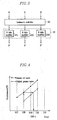
- the luminance control of the luminance controller 42 is described with reference to Fig. 2A, which is an exemplary graph illustrating luminance of an LCD as function of gray.
- the luminance represented by a predetermined gray D is smaller than 80 cd/m 2
- the gray D+ ⁇ D represent the luminance of 80 cd/m 2
- the luminance controller 42 performs the luminance control by adding the value ⁇ D into input image data such that the luminance represented by the gray D of the predetermined input image data reach 80 cd/m 2 . Therefore, the luminance control moves the solid luminance curve in a direction A to a dotted luminance curve.
- the predetermined gray D is preferably a maximum gray.
- the gamma converter 43 converts a gamma characteristic of the image data from the luminance controller 42 such that it is adapted to a gamma 2.2 curve, and it outputs the converted image data R'G'B' to the data driver 30.
- the gamma converter 42 may perform the gamma conversion by way of a look-up table (LUT) or a mathematical operation realized on an application specific integrated circuit (ASIC).
- LUT look-up table
- ASIC application specific integrated circuit
- the configuration shown in Fig. 1 is obtained when using a look-up table.
- the look-up table includes a mapping from the original (input) image data RGB to the converted (output) image data R'G'B'.
- the gamma converter 42 retrieves a converted data corresponding to an input image data from the look-up table, and it output the converted image data.
- Fig. 1 shows that the bit number (n bits) of the converted image data R'G'B' is equal to the bit number (n bits) of the original image data RGB, the bit number of the converted image data RGB may be larger than the bit number of the original image data RGB in order to enhance the precision of the gamma conversion.
- Fig. 2B shows an exemplary graph illustrating gamma curves of an LCD including an original gamma curve and a gamma 2.2 curve for a standard RGB (sRGB) color space.
- a horizontal axis indicates a normalized input gray level while a vertical axis indicates a normalized luminance.
- the data driver 30 receives and stores the converted image data R'G'B' from the gamma converter 43 of the signal controller 40 in synchronization with the control signals HCLK and STH.
- the data driver 30 receives a plurality of gray voltages Vgray, which are analog voltages to be actually applied to the liquid crystal panel assembly 10, from the voltage generator 50.
- the data driver 30 selects the gray voltages Vgray corresponding to the image data R'G'B' for the respective pixels, and outputs the selected gray voltages as the data voltages to the liquid crystal panel assembly 10 in response to the load signal LOAD.
- the gate driver 20 receives the gate clock signal Gate clock, the output enable signal OE, and the vertical synchronization start signal STV from the signal controller 40, and it also receives gate voltages Vgate from the voltage generator 50.
- the gate driver 20 sequentially outputs the gate voltages for selecting the gate lines on the liquid crystal panel assembly 10 in accordance with the output enable signal OE and the gate clock signal Gate clock, thereby sequentially scanning the gate lines on the liquid crystal panel assembly 10.
- the lamp 60 and the inverter 70 form a backlight for the liquid crystal panel assembly 10, and the inverter 70 controls the light emission of the lamp 60.
- the inverter 70 controls the lamp 60 with a luminance of 80cd/m 2 or more to fulfill the luminance requirement of the sRGB color space.
- the pixels connected to the gate line become in a write-enable state to be applied with the data voltages through the data lines.
- the pixels display predetermined luminance levels corresponding to the data voltages and a desired image is displayed on an entire screen in such a way.
- Fig. 3 is a detailed block diagram of the luminance controller 42 and the gamma converter 43 shown in Fig. 1, and Fig. 4 is a graph showing a gamma 2.2 curve and an original gamma curve for illustrating the conversion of the gamma curve at the gamma converter 43 shown in Fig. 3.
- the gamma converter 43 includes an R data modifier 431, a G data modifier 432, and a B data modifier 433.
- the data modifiers 431-433 perform the conversion of the gamma characteristics in relation to the respective RGB colors.
- each data modifier 431-433 maps an input image data representing a luminance level on the gamma 2.2 curve into an output image data representing the same luminance level on the original gamma curve.
- the gray level of the input image data is 128.
- the luminance of the 128-th gray level on the original gamma curve is different from the luminance of the 128-th gray level on the gamma 2.2 curve.
- the 129.4-th gray level on the original gamma curve represents the same luminance as the 128-th gray level on the gamma 2.2 curve.
- Each data modifier 431-433 maps the input image data with the 128-th gray level into the output image data with the 129.4-th gray level.
- each data modifier 431-433 includes a look-up table including a map between gray levels on the gamma 2.2 curve and gray levels on the original gamma curve, which represent equal luminance.
- the look-up tables for the data modifiers 431-433 may be implemented in respective non-volatile memories such as ROM (read only memory) or implemented in one ROM.
- ROM read only memory
- the bit number of the output image data is larger than that of the input image data such that decimals under the decimal point of the gray levels as shown in Fig. 4 can be expressed.
- Figs. 5 and 6 are block diagrams of an LCD according to other embodiments of the present invention.
- the LCD shown in Fig. 5 further includes a ROM controller 44 and an external target image data storage 45 in addition to a gamma converter 43.
- the gamma converter 43 includes R, G and B data modifiers 431-433, each including a volatile memory such as a random access memory (RAM).
- the external target image data storage 45 stores a look-up table including a map between gray levels on the gamma 2.2 curve and gray levels on the original gamma curve for each color, which represent equal luminance.
- the ROM controller 44 loads the look-up table in the storage 45 into the R, G and B data modifiers 431-433. Since the other operations are similar to those shown in Fig. 3, the description thereof is omitted here.
- this embodiment easily copes with the alteration of the panel assembly 10 without changing the gamma converter 43.
- the LCD shown in Fig. 6 further includes an internal target image data storage 46 as well as a ROM controller 44, an external target image data storage 45 in addition to a gamma converter 43 as compared with the LCD shown in Fig. 5.
- the gamma converter 43 also includes R, G and B data modifiers 431-433, each including a volatile memory such as a random access memory (RAM).
- RAM random access memory
- the internal target image data storage 46 stores a look-up table including the above-described map.
- the ROM controller 44 loads the look-up table stored in the external storage 45 or in the internal storage 46 into the R, G and B data modifiers 431-433. Other operations are similar to those shown in Fig. 3, and hence, description thereof will be omitted here.
- Fig. 7 is a graph illustrating the gray difference between input (original) image data and corresponding output (target) image data as function of the gray of the input image data in an LCD according to an embodiment of the present invention
- Fig. 8 is a flowchart illustrating an exemplary gamma conversion process by way of mathematical operation in an LCD according to an embodiment of the present invention.
- the image data RGB are 8 bit signals capable of representing 256 grays.
- the 8 bit input data is multiplied by "4" to be converted into 10 bit data and is added to the calculated value ⁇ R (S508).
- blue output image data B' can be calculated based on Relation 2.
- the gamma conversion by way of a mathematical operation does not require a memory for storing a look-up table.
- the storage capacity of ROM or RAM required for storing the look-up table is considerably great. For instance, the storage capacity of 6144 (3 ⁇ 256 ⁇ 8) bits are required for 8 bit image data. Accordingly, the gamma conversion according to this embodiment removes a large amount of storage capacity and reduces the power consumption due to the memory.
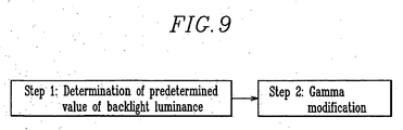
- Fig. 9 illustrates a method of driving an LCD in a sRGB color space according to an embodiment of the present invention.
- a method of driving an LCD including a backlight unit includes a first step for controlling the backlight and a second step for gamma correction.
- the backlight unit includes at least one lamp and an inverter for controlling the lamp.
- the inverter is controlled such that the lamp emits light with a luminance equal to or larger than 80 cd/m 2 , which is required for the sRGB color space.
- the second step includes the substeps of luminance control and gamma conversion as described above.
- the luminance of the image data is controlled such that the luminance level represented by a predetermined gray level of image data be 80cd/m 2 , and the gamma characteristic of the input image data are converted to be adapted to the gamma 2.2 curve.
- the luminance of the backlight is determined to be a specific value larger than 80cd/m 2 , and the luminance of the image data is controlled such that the luminance of the input image data satisfies 80cd/m 2 at the specific image data value.
- the sRGB mode can be realized with the LCD, and the display quality of the LCD can be improved.
Landscapes
- Engineering & Computer Science (AREA)
- Physics & Mathematics (AREA)
- General Physics & Mathematics (AREA)
- Theoretical Computer Science (AREA)
- Computer Hardware Design (AREA)
- Crystallography & Structural Chemistry (AREA)
- Chemical & Material Sciences (AREA)
- Nonlinear Science (AREA)
- Mathematical Physics (AREA)
- Optics & Photonics (AREA)
- Control Of Indicators Other Than Cathode Ray Tubes (AREA)
- Liquid Crystal Display Device Control (AREA)
- Liquid Crystal (AREA)
- Transforming Electric Information Into Light Information (AREA)
Abstract
Description


Claims (10)
- A liquid crystal display comprising:a signal controller including a luminance controller processing input image data with respective grays such that the luminance represented by a predetermined gray of the input image data be about 80 cd/m2, and a gamma converter outputting output image data have gamma characteristic adapted to a gamma 2.2 curve based on input image data;a data driver selecting and outputting gray voltages corresponding to the image data from the signal controller; andan inverter controlling a lamp such that the lamp emits light with luminance equal to or larger than 80 cd/m2.
- The liquid crystal display of claim 1, wherein the processing of the luminance controller includes addition of a predetermined data value to the input image data such that the luminance represented by the predetermined gray of the input image data be 80cd/m2.
- The liquid crystal display of claim 1, wherein the gamma converter comprises an R data modifier, a G data modifier and a B data modifier for performing the gamma conversion for the input image data for respective red, green and blue colors, and each of the data modifiers maps the input image data into output image data having a gamma characteristic adapted to the gamma 2.2 curve.
- The liquid crystal display of claim 3, wherein the data modifiers include a nonvolatile memory.
- The liquid crystal display of claim 1, wherein the gamma converter comprises an R data modifier, a G data modifier and a B data modifier for performing the gamma conversion for the input image data for respective red, green and blue colors, the liquid crystal display further comprises a target image data storage storing a map from the input image data into output image data having a gamma characteristic adapted to the gamma 2.2 curve and a controller loading the map stored in the target image data storage into the data modifiers, and the data modifiers select the output image data corresponding to the input image data from the loaded map and outputting the selected output image data.
- The liquid crystal display of claim 5, wherein the data modifiers comprise a volatile memory, and the target image data storage comprises a nonvolatile memory element.
- The liquid crystal display of claim 5, wherein the target image data storage includes a nonvolatile memory in the signal controller and a nonvolatile memory element provided external to the signal controller.
- The liquid crystal display of claim 1, wherein the gamma converter obtains the output image data from the input image data by way of a mathematical operation.
- A method of driving a liquid crystal display, the method comprising:controlling luminance of a backlight to be larger than about 80 cd/m2;controlling luminance of image data such that the luminance level represented by a predetermined gray of input image data be about 80 cd/m2; andconverting gamma characteristic of the input image data to be adapted to a gamma 2.2 curve.
- The method of claim 9, wherein the gamma characteristic conversion includes a mathematical operation realized on an application specific integrated circuit (ASIC).
Applications Claiming Priority (2)
| Application Number | Priority Date | Filing Date | Title |
|---|---|---|---|
| KR2002070050 | 2002-11-12 | ||
| KR1020020070050A KR20040041940A (en) | 2002-11-12 | 2002-11-12 | Liquid crystal display and driving method thereof |
Publications (3)
| Publication Number | Publication Date |
|---|---|
| EP1420385A2 true EP1420385A2 (en) | 2004-05-19 |
| EP1420385A3 EP1420385A3 (en) | 2007-04-18 |
| EP1420385B1 EP1420385B1 (en) | 2013-01-16 |
Family
ID=32171625
Family Applications (1)
| Application Number | Title | Priority Date | Filing Date |
|---|---|---|---|
| EP03026083A Expired - Lifetime EP1420385B1 (en) | 2002-11-12 | 2003-11-12 | Liquid crystal display |
Country Status (6)
| Country | Link |
|---|---|
| US (2) | US7365723B2 (en) |
| EP (1) | EP1420385B1 (en) |
| JP (1) | JP2004163946A (en) |
| KR (1) | KR20040041940A (en) |
| CN (1) | CN100369099C (en) |
| TW (1) | TW200414098A (en) |
Cited By (4)
| Publication number | Priority date | Publication date | Assignee | Title |
|---|---|---|---|---|
| WO2006050096A1 (en) * | 2004-10-28 | 2006-05-11 | Qualcomm Incorporated | Apparatus, system, and method for optimizing gamma curves for digital image devices |
| CN101777308B (en) * | 2009-01-09 | 2012-03-21 | 联咏科技股份有限公司 | Driving method and display device capable of improving image brightness and reducing picture distortion |
| CN102981351A (en) * | 2011-09-05 | 2013-03-20 | 卡西欧计算机株式会社 | Projection apparatus and projection control method |
| CN115151971A (en) * | 2020-01-31 | 2022-10-04 | 高通股份有限公司 | Dynamic gamma curve usage for display |
Families Citing this family (14)
| Publication number | Priority date | Publication date | Assignee | Title |
|---|---|---|---|---|
| KR20040041940A (en) * | 2002-11-12 | 2004-05-20 | 삼성전자주식회사 | Liquid crystal display and driving method thereof |
| KR100947776B1 (en) * | 2003-06-17 | 2010-03-15 | 엘지디스플레이 주식회사 | Lamp driving device and driving method of liquid crystal display module |
| CN100397477C (en) * | 2005-01-17 | 2008-06-25 | 胜华科技股份有限公司 | Image processing device and method for improving brightness and image quality of display panel |
| TWI330270B (en) * | 2005-03-29 | 2010-09-11 | Chi Mei Optoelectronics Corp | Region-based displayer and display method thereof |
| JP2007139842A (en) | 2005-11-15 | 2007-06-07 | Nec Electronics Corp | Display device, data driver ic, and timing controller |
| CN101021999B (en) * | 2006-02-15 | 2010-12-22 | 奇美电子股份有限公司 | Zone division type display device and displaying method thereof |
| US20070236437A1 (en) * | 2006-03-30 | 2007-10-11 | Hannstar Display Corp. | Dynamic gamma control method for LCD |
| KR100891220B1 (en) * | 2007-09-12 | 2009-04-01 | 주식회사 동부하이텍 | Control signal generator for removing driver offset |
| KR20090037210A (en) * | 2007-10-11 | 2009-04-15 | 삼성전자주식회사 | Display Device and Gamma Data Adjustment Method |
| TWI393089B (en) * | 2008-03-21 | 2013-04-11 | Chimei Innolux Corp | Method of storing gamma look-up table |
| KR20150081174A (en) * | 2014-01-03 | 2015-07-13 | 삼성디스플레이 주식회사 | Liquid crystal display apparatus and the drivinig method of the same |
| KR102465008B1 (en) * | 2016-01-20 | 2022-11-09 | 삼성디스플레이 주식회사 | Spot compensating apparatus, method of compensating spot, and display system having the spot compensating apparatus |
| KR20180071821A (en) * | 2016-12-20 | 2018-06-28 | 삼성전자주식회사 | Display apparatus and driving method thereof |
| US12512037B1 (en) * | 2024-06-26 | 2025-12-30 | Himax Technologies Limited | Image display device configured to convert row display data into update instructions, image transmission system, and updating method |
Family Cites Families (37)
| Publication number | Priority date | Publication date | Assignee | Title |
|---|---|---|---|---|
| JPH0514654A (en) * | 1991-07-04 | 1993-01-22 | Kowa Co | Image signal processor |
| JP3071590B2 (en) * | 1993-01-05 | 2000-07-31 | 日本電気株式会社 | Liquid crystal display device |
| JP3107260B2 (en) * | 1993-03-02 | 2000-11-06 | 株式会社富士通ゼネラル | Color display |
| JPH0772832A (en) * | 1993-06-30 | 1995-03-17 | Fujitsu Ltd | γ correction circuit, liquid crystal driving device, image display method and liquid crystal display device |
| JP3406943B2 (en) * | 1994-10-20 | 2003-05-19 | キヤノン株式会社 | Display control method and device and display device |
| KR100205934B1 (en) | 1995-05-31 | 1999-07-01 | 김영남 | Color Plasma Display Device |
| JPH09128330A (en) * | 1995-11-06 | 1997-05-16 | Sony Corp | Video display |
| US6188380B1 (en) * | 1997-02-03 | 2001-02-13 | Nanao Corporation | Photodetector of liquid crystal display and luminance control device using the same |
| JPH1131589A (en) | 1997-07-09 | 1999-02-02 | Matsushita Electric Ind Co Ltd | Injection type electroluminescent device and manufacturing method thereof |
| JP3247643B2 (en) * | 1997-09-10 | 2002-01-21 | インターナショナル・ビジネス・マシーンズ・コーポレーション | Liquid crystal display device |
| KR100269256B1 (en) | 1997-09-11 | 2000-10-16 | 정선종 | How to automatically monitor |
| JPH11187285A (en) * | 1997-12-17 | 1999-07-09 | Sanyo Electric Co Ltd | Image data processor |
| US6278496B1 (en) * | 1997-10-09 | 2001-08-21 | Sanyo Electric Co., Ltd. | Digital correction circuit and image data processing apparatus equipped with a digital correction circuit |
| JPH11305734A (en) * | 1998-04-17 | 1999-11-05 | Hitachi Ltd | Liquid crystal display device |
| US6611249B1 (en) * | 1998-07-22 | 2003-08-26 | Silicon Graphics, Inc. | System and method for providing a wide aspect ratio flat panel display monitor independent white-balance adjustment and gamma correction capabilities |
| JP4189062B2 (en) * | 1998-07-06 | 2008-12-03 | セイコーエプソン株式会社 | Electronics |
| US6215468B1 (en) * | 1998-11-13 | 2001-04-10 | Philips Electronics North America Corporation | Circuit for converting an 8-bit input video signal into a 10-bit gamma corrected output video signal |
| HK1043196A1 (en) * | 1999-03-16 | 2002-09-06 | Zms有限责任公司 | Precision integral articles |
| JP2001335516A (en) | 1999-11-08 | 2001-12-04 | Idemitsu Kosan Co Ltd | Organic electroluminescence device |
| JP3412583B2 (en) * | 1999-11-08 | 2003-06-03 | 日本電気株式会社 | Driving method and circuit of color liquid crystal display |
| JP3939066B2 (en) | 2000-03-08 | 2007-06-27 | 富士通日立プラズマディスプレイ株式会社 | Color plasma display device |
| JP2001284060A (en) | 2000-03-29 | 2001-10-12 | Honda Motor Co Ltd | Transparent electrode and organic electroluminescence device |
| JP2001290174A (en) * | 2000-04-05 | 2001-10-19 | Canon Inc | Liquid crystal device |
| JP4980508B2 (en) * | 2000-04-24 | 2012-07-18 | エーユー オプトロニクス コーポレイション | Liquid crystal display device, monochrome liquid crystal display device, controller, and image conversion method |
| US6628828B1 (en) * | 2000-04-24 | 2003-09-30 | Microsoft Corporation | System and method for performing a recoloring operation sequence on color objects |
| US6580224B2 (en) * | 2000-06-05 | 2003-06-17 | Kabushiki Kaisha Toshiba | Backlight for color liquid crystal, color liquid crystal display device, and EL element for backlight of color liquid crystal device |
| JP2001351425A (en) * | 2000-06-08 | 2001-12-21 | Fujitsu Ltd | Backlight device and liquid crystal display device |
| JP2002116750A (en) * | 2000-10-05 | 2002-04-19 | Sharp Corp | Color conversion circuit, color conversion method, and color image display device |
| JP2002202767A (en) * | 2000-10-25 | 2002-07-19 | Samsung Electronics Co Ltd | Liquid crystal display device, its driving device and its method |
| KR100415510B1 (en) * | 2001-03-15 | 2004-01-16 | 삼성전자주식회사 | Liquid crystal display device with a function of adaptive brightness intensifier and method for therefor |
| KR100363540B1 (en) * | 2000-12-21 | 2002-12-05 | 삼성전자 주식회사 | Fast driving liquid crystal display and gray voltage generating circuit for the same |
| JP2002323876A (en) * | 2001-04-24 | 2002-11-08 | Nec Corp | Picture display method in liquid crystal display and liquid crystal display device |
| JP2003015612A (en) * | 2001-06-29 | 2003-01-17 | Nec Corp | Driving method for liquid crystal display, liquid crystal display device and monitor |
| US7030846B2 (en) * | 2001-07-10 | 2006-04-18 | Samsung Electronics Co., Ltd. | Color correction liquid crystal display and method of driving same |
| KR100910557B1 (en) * | 2002-11-12 | 2009-08-03 | 삼성전자주식회사 | LCD and its driving method |
| KR20040041941A (en) * | 2002-11-12 | 2004-05-20 | 삼성전자주식회사 | Liquid crystal display and driving method thereof |
| KR20040041940A (en) * | 2002-11-12 | 2004-05-20 | 삼성전자주식회사 | Liquid crystal display and driving method thereof |
-
2002
- 2002-11-12 KR KR1020020070050A patent/KR20040041940A/en not_active Ceased
-
2003
- 2003-11-11 JP JP2003380963A patent/JP2004163946A/en active Pending
- 2003-11-12 TW TW092131713A patent/TW200414098A/en unknown
- 2003-11-12 CN CNB200310120911XA patent/CN100369099C/en not_active Expired - Lifetime
- 2003-11-12 US US10/704,828 patent/US7365723B2/en not_active Expired - Lifetime
- 2003-11-12 EP EP03026083A patent/EP1420385B1/en not_active Expired - Lifetime
-
2008
- 2008-03-28 US US12/057,738 patent/US20090021535A1/en not_active Abandoned
Cited By (7)
| Publication number | Priority date | Publication date | Assignee | Title |
|---|---|---|---|---|
| WO2006050096A1 (en) * | 2004-10-28 | 2006-05-11 | Qualcomm Incorporated | Apparatus, system, and method for optimizing gamma curves for digital image devices |
| US7545421B2 (en) | 2004-10-28 | 2009-06-09 | Qualcomm Incorporated | Apparatus, system, and method for optimizing gamma curves for digital image devices |
| CN101088278B (en) * | 2004-10-28 | 2012-11-14 | 高通股份有限公司 | Apparatus and method for optimizing gamma curves for digital image devices |
| CN101777308B (en) * | 2009-01-09 | 2012-03-21 | 联咏科技股份有限公司 | Driving method and display device capable of improving image brightness and reducing picture distortion |
| CN102981351A (en) * | 2011-09-05 | 2013-03-20 | 卡西欧计算机株式会社 | Projection apparatus and projection control method |
| CN102981351B (en) * | 2011-09-05 | 2015-01-28 | 卡西欧计算机株式会社 | Projection apparatus and projection control method |
| CN115151971A (en) * | 2020-01-31 | 2022-10-04 | 高通股份有限公司 | Dynamic gamma curve usage for display |
Also Published As
| Publication number | Publication date |
|---|---|
| TW200414098A (en) | 2004-08-01 |
| US20050057472A1 (en) | 2005-03-17 |
| EP1420385A3 (en) | 2007-04-18 |
| JP2004163946A (en) | 2004-06-10 |
| EP1420385B1 (en) | 2013-01-16 |
| CN100369099C (en) | 2008-02-13 |
| US20090021535A1 (en) | 2009-01-22 |
| CN1512475A (en) | 2004-07-14 |
| KR20040041940A (en) | 2004-05-20 |
| US7365723B2 (en) | 2008-04-29 |
Similar Documents
| Publication | Publication Date | Title |
|---|---|---|
| US20090021535A1 (en) | Liquid crystal display and method fo driving thereof | |
| US20060208983A1 (en) | Liquid crystal display and driving method thereof | |
| US20060145979A1 (en) | Liquid crystal display and driving method thereof | |
| US10699615B2 (en) | Application processor and display device including the same | |
| CN111243512B (en) | Gray-scale data compensation method and device and driving chip | |
| EP2339570B1 (en) | Liquid crystal display with RGBW pixels and dynamic backlight control | |
| JP4929315B2 (en) | Liquid crystal display | |
| KR100859514B1 (en) | Liquid crystal display and its driving device | |
| US7468716B2 (en) | Modifying gray voltage signals in a display device | |
| KR101825214B1 (en) | Liquid crystal display device and driving method thereof | |
| US20220189413A1 (en) | Display apparatus and method of driving display panel using the same | |
| CN109817184B (en) | Apparatus and method for chromatic aberration correction | |
| US20080211758A1 (en) | Liquid crystal display having gray voltages and driving apparatus and method thereof | |
| KR20030073390A (en) | A liquid crystal display for improving dynamic contrast and a method for generating gamma voltages for the liquid crystal display | |
| US20210166612A1 (en) | Flexible display device, and method of operating a flexible display device | |
| JP2023108808A (en) | CURRENT LIMITING CIRCUIT, DISPLAY DEVICE AND CURRENT LIMITING METHOD | |
| US20050062702A1 (en) | Display device with reduced flickering | |
| US12444389B2 (en) | Mura compensation device and mura compensation system including the same | |
| US20070052984A1 (en) | Apparatus and method of converting image signal for four color display device | |
| KR20080043604A (en) | Display device and driving method thereof |
Legal Events
| Date | Code | Title | Description |
|---|---|---|---|
| PUAI | Public reference made under article 153(3) epc to a published international application that has entered the european phase |
Free format text: ORIGINAL CODE: 0009012 |
|
| AK | Designated contracting states |
Kind code of ref document: A2 Designated state(s): AT BE BG CH CY CZ DE DK EE ES FI FR GB GR HU IE IT LI LU MC NL PT RO SE SI SK TR |
|
| AX | Request for extension of the european patent |
Extension state: AL LT LV MK |
|
| PUAL | Search report despatched |
Free format text: ORIGINAL CODE: 0009013 |
|
| AK | Designated contracting states |
Kind code of ref document: A3 Designated state(s): AT BE BG CH CY CZ DE DK EE ES FI FR GB GR HU IE IT LI LU MC NL PT RO SE SI SK TR |
|
| AX | Request for extension of the european patent |
Extension state: AL LT LV MK |
|
| RIC1 | Information provided on ipc code assigned before grant |
Ipc: G09G 3/36 20060101AFI20070309BHEP |
|
| 17P | Request for examination filed |
Effective date: 20071011 |
|
| 17Q | First examination report despatched |
Effective date: 20071115 |
|
| AKX | Designation fees paid |
Designated state(s): DE FR GB |
|
| RIN1 | Information on inventor provided before grant (corrected) |
Inventor name: KIM, JONG-SEON Inventor name: KIM, CHANG-YEONG Inventor name: PARK, DOO-SIK Inventor name: CHOH, HEUI-KEUN Inventor name: LEE, SEUNG-WOO Inventor name: YU YUN-JU |
|
| RTI1 | Title (correction) |
Free format text: LIQUID CRYSTAL DISPLAY |
|
| GRAP | Despatch of communication of intention to grant a patent |
Free format text: ORIGINAL CODE: EPIDOSNIGR1 |
|
| RAP1 | Party data changed (applicant data changed or rights of an application transferred) |
Owner name: SAMSUNG ELECTRONICS CO., LTD. |
|
| GRAS | Grant fee paid |
Free format text: ORIGINAL CODE: EPIDOSNIGR3 |
|
| RAP1 | Party data changed (applicant data changed or rights of an application transferred) |
Owner name: SAMSUNG DISPLAY CO., LTD. |
|
| GRAA | (expected) grant |
Free format text: ORIGINAL CODE: 0009210 |
|
| AK | Designated contracting states |
Kind code of ref document: B1 Designated state(s): DE FR GB |
|
| REG | Reference to a national code |
Ref country code: GB Ref legal event code: FG4D |
|
| REG | Reference to a national code |
Ref country code: DE Ref legal event code: R096 Ref document number: 60343117 Country of ref document: DE Effective date: 20130314 |
|
| PLBE | No opposition filed within time limit |
Free format text: ORIGINAL CODE: 0009261 |
|
| STAA | Information on the status of an ep patent application or granted ep patent |
Free format text: STATUS: NO OPPOSITION FILED WITHIN TIME LIMIT |
|
| 26N | No opposition filed |
Effective date: 20131017 |
|
| REG | Reference to a national code |
Ref country code: DE Ref legal event code: R097 Ref document number: 60343117 Country of ref document: DE Effective date: 20131017 |
|
| REG | Reference to a national code |
Ref country code: FR Ref legal event code: PLFP Year of fee payment: 13 |
|
| REG | Reference to a national code |
Ref country code: FR Ref legal event code: PLFP Year of fee payment: 14 |
|
| REG | Reference to a national code |
Ref country code: FR Ref legal event code: PLFP Year of fee payment: 15 |
|
| REG | Reference to a national code |
Ref country code: FR Ref legal event code: PLFP Year of fee payment: 16 |
|
| REG | Reference to a national code |
Ref country code: DE Ref legal event code: R082 Ref document number: 60343117 Country of ref document: DE Representative=s name: SCHIEBER - FARAGO PATENTANWAELTE, DE Ref country code: DE Ref legal event code: R082 Ref document number: 60343117 Country of ref document: DE Representative=s name: FARAGO PATENTANWALTSGESELLSCHAFT MBH, DE |
|
| REG | Reference to a national code |
Ref country code: DE Ref legal event code: R082 Ref document number: 60343117 Country of ref document: DE Representative=s name: SCHIEBER - FARAGO PATENTANWAELTE, DE |
|
| PGFP | Annual fee paid to national office [announced via postgrant information from national office to epo] |
Ref country code: FR Payment date: 20221020 Year of fee payment: 20 |
|
| PGFP | Annual fee paid to national office [announced via postgrant information from national office to epo] |
Ref country code: GB Payment date: 20221020 Year of fee payment: 20 Ref country code: DE Payment date: 20220620 Year of fee payment: 20 |
|
| P01 | Opt-out of the competence of the unified patent court (upc) registered |
Effective date: 20230515 |
|
| REG | Reference to a national code |
Ref country code: DE Ref legal event code: R071 Ref document number: 60343117 Country of ref document: DE |
|
| REG | Reference to a national code |
Ref country code: GB Ref legal event code: PE20 Expiry date: 20231111 |
|
| PG25 | Lapsed in a contracting state [announced via postgrant information from national office to epo] |
Ref country code: GB Free format text: LAPSE BECAUSE OF EXPIRATION OF PROTECTION Effective date: 20231111 |
|
| PG25 | Lapsed in a contracting state [announced via postgrant information from national office to epo] |
Ref country code: GB Free format text: LAPSE BECAUSE OF EXPIRATION OF PROTECTION Effective date: 20231111 |