EP1420081A2 - Thin film formation apparatus and thin film formation method employing the apparatus - Google Patents
Thin film formation apparatus and thin film formation method employing the apparatus Download PDFInfo
- Publication number
- EP1420081A2 EP1420081A2 EP03022925A EP03022925A EP1420081A2 EP 1420081 A2 EP1420081 A2 EP 1420081A2 EP 03022925 A EP03022925 A EP 03022925A EP 03022925 A EP03022925 A EP 03022925A EP 1420081 A2 EP1420081 A2 EP 1420081A2
- Authority
- EP
- European Patent Office
- Prior art keywords
- electrodes
- thin film
- film formation
- electrode
- formation apparatus
- Prior art date
- Legal status (The legal status is an assumption and is not a legal conclusion. Google has not performed a legal analysis and makes no representation as to the accuracy of the status listed.)
- Granted
Links
Images



Classifications
-
- H—ELECTRICITY
- H01—ELECTRIC ELEMENTS
- H01J—ELECTRIC DISCHARGE TUBES OR DISCHARGE LAMPS
- H01J37/00—Discharge tubes with provision for introducing objects or material to be exposed to the discharge, e.g. for the purpose of examination or processing thereof
- H01J37/32—Gas-filled discharge tubes
- H01J37/32009—Arrangements for generation of plasma specially adapted for examination or treatment of objects, e.g. plasma sources
-
- C—CHEMISTRY; METALLURGY
- C23—COATING METALLIC MATERIAL; COATING MATERIAL WITH METALLIC MATERIAL; CHEMICAL SURFACE TREATMENT; DIFFUSION TREATMENT OF METALLIC MATERIAL; COATING BY VACUUM EVAPORATION, BY SPUTTERING, BY ION IMPLANTATION OR BY CHEMICAL VAPOUR DEPOSITION, IN GENERAL; INHIBITING CORROSION OF METALLIC MATERIAL OR INCRUSTATION IN GENERAL
- C23C—COATING METALLIC MATERIAL; COATING MATERIAL WITH METALLIC MATERIAL; SURFACE TREATMENT OF METALLIC MATERIAL BY DIFFUSION INTO THE SURFACE, BY CHEMICAL CONVERSION OR SUBSTITUTION; COATING BY VACUUM EVAPORATION, BY SPUTTERING, BY ION IMPLANTATION OR BY CHEMICAL VAPOUR DEPOSITION, IN GENERAL
- C23C16/00—Chemical coating by decomposition of gaseous compounds, without leaving reaction products of surface material in the coating, i.e. chemical vapour deposition [CVD] processes
- C23C16/44—Chemical coating by decomposition of gaseous compounds, without leaving reaction products of surface material in the coating, i.e. chemical vapour deposition [CVD] processes characterised by the method of coating
- C23C16/50—Chemical coating by decomposition of gaseous compounds, without leaving reaction products of surface material in the coating, i.e. chemical vapour deposition [CVD] processes characterised by the method of coating using electric discharges
- C23C16/505—Chemical coating by decomposition of gaseous compounds, without leaving reaction products of surface material in the coating, i.e. chemical vapour deposition [CVD] processes characterised by the method of coating using electric discharges using radio frequency discharges
- C23C16/509—Chemical coating by decomposition of gaseous compounds, without leaving reaction products of surface material in the coating, i.e. chemical vapour deposition [CVD] processes characterised by the method of coating using electric discharges using radio frequency discharges using internal electrodes
- C23C16/5096—Flat-bed apparatus
-
- H—ELECTRICITY
- H01—ELECTRIC ELEMENTS
- H01J—ELECTRIC DISCHARGE TUBES OR DISCHARGE LAMPS
- H01J37/00—Discharge tubes with provision for introducing objects or material to be exposed to the discharge, e.g. for the purpose of examination or processing thereof
- H01J37/32—Gas-filled discharge tubes
- H01J37/32009—Arrangements for generation of plasma specially adapted for examination or treatment of objects, e.g. plasma sources
- H01J37/32082—Radio frequency generated discharge
-
- H—ELECTRICITY
- H01—ELECTRIC ELEMENTS
- H01J—ELECTRIC DISCHARGE TUBES OR DISCHARGE LAMPS
- H01J37/00—Discharge tubes with provision for introducing objects or material to be exposed to the discharge, e.g. for the purpose of examination or processing thereof
- H01J37/32—Gas-filled discharge tubes
- H01J37/32431—Constructional details of the reactor
- H01J37/32532—Electrodes
- H01J37/32568—Relative arrangement or disposition of electrodes; moving means
-
- H—ELECTRICITY
- H01—ELECTRIC ELEMENTS
- H01J—ELECTRIC DISCHARGE TUBES OR DISCHARGE LAMPS
- H01J37/00—Discharge tubes with provision for introducing objects or material to be exposed to the discharge, e.g. for the purpose of examination or processing thereof
- H01J37/32—Gas-filled discharge tubes
- H01J37/32431—Constructional details of the reactor
- H01J37/32715—Workpiece holder
- H01J37/32724—Temperature
Definitions
- the present invention relates to a thin film formation apparatus and a thin film formation method employing the apparatus. More particularly, the invention relates to a thin film formation apparatus and a thin film formation method which utilize a plasma CVD process.
- One known method for forming a silicon thin film on a substrate is a plasma CVD process in which a reactant gas is decomposed by a plasma energy and the resulting material is deposited on a substrate. Further, a plasma CVD apparatus is known to be employed for this process.
- the plasma CVD apparatus typically includes a reaction chamber adapted to be evacuated to vacuum, a gas introduction section for introducing a reactant gas into the reaction chamber, an evacuation section for exhausting the reactant gas from the reaction chamber, a planar anode electrode and a planar cathode electrode disposed in opposed spaced relation, and a high frequency power source for applying high frequency power between the anode electrode and the cathode electrode (see, for example, US Patent No. 4,264,393).
- the anode electrode has a surface on which a substrate to be formed with a film is placed in opposed relation to the cathode electrode, and includes a heater incorporated therein for heating the substrate.
- the cathode electrode has a hollow inside and a surface formed with a multiplicity of through-holes in opposed relation to the anode electrode, and is adapted to eject the gas supplied from the gas introduction section through the through-holes.
- the anode electrode and the cathode electrode are firmly fixed to the reaction chamber so that the spacing therebetween can accurately be maintained.
- the anode electrode on which the substrate is placed is heated up to about 300° C, and the cathode electrode opposed to the anode electrode is also heated by heat radiation from the anode electrode. At this time, the anode electrode and the cathode electrode are thermally expanded to be deformed, so that the spacing therebetween is varied. If the spacing between the anode electrode and the cathode electrode is varied, the apparatus fails to provide desired performance, thereby adversely affecting a film thickness distribution.
- the present invention is directed to a thin film formation apparatus which is capable of preventing the thermal deformation of the anode electrode and the cathode electrode when the anode electrode and the cathode electrode are heated, and suppressing the variation in the spacing between the anode electrode and the cathode electrode.
- a thin film formation apparatus for forming a thin film on a substrate, which comprises: a reaction chamber; a gas introduction section for introducing a reactant gas into the reaction chamber; an evacuation section for exhausting the reactant gas from the reaction chamber; first and second planar electrodes provided in the reaction chamber; first and second support members which respectively support the first and second electrodes in parallel relation; a high frequency power source for applying high frequency power between the first and second electrodes; and a heating section for heating one of the first and second electrodes; wherein the substrate is placed on the heated electrode, and at least one of the first and second electrodes is supported movably in the direction of thermal expansion by the corresponding support member.
- the first and second support members respectively support the first and second electrodes, and at least one of the first and second electrodes is movable in the thermal expansion direction. Therefore, when the first and second electrodes are heated to be thermally expanded, the at least one electrode moves in the thermal expansion direction, whereby the thermal expansion can be relieved. As a result, a variation in the spacing between the first and second electrodes can be reduced, thereby improving the performance of the apparatus. Since the at least one of the first and second electrodes is supported movably in the thermal expansion direction, the electrodes can easily be removed from the apparatus in the maintenance of the apparatus. This facilitates the maintenance of the plasma CVD apparatus.
- a thin film formation apparatus for forming a thin film on a substrate comprises: a reaction chamber; a gas introduction section for introducing a reactant gas into the reaction chamber; an evacuation section for exhausting the reactant gas from the reaction chamber; first and second planar electrodes provided in the reaction chamber; first and second support members which respectively support the first and second electrodes in parallel relation; a high frequency power source for applying high frequency power between the first and second electrodes; and a heating section for heating one of the first and second electrodes; wherein the substrate is placed on the heated electrode, and at least one of the first and second electrodes is supported movably in the direction of thermal expansion by the corresponding support member.
- the inventive thin film formation apparatus is employed, for example, for formation of a silicon thin film by a plasma CVD process.
- the silicon thin film include crystalline to amorphous thin films essentially comprising silicon.
- the reactant gas comprises a silicon containing gas.
- Specific examples of the reactant gas include silane (SiH 4 ) and disilane (Si 2 H 6 ), which may be diluted by hydrogen (H 2 ) or helium (He).
- the silicon thin film to be formed by the inventive thin film formation apparatus examples include a silicon carbide (SiC) film, a silicon nitride (SiN) film, a silicon oxide (SiO) film and a SiGe film.
- the reactant gas further comprises a carbon containing gas such as CH 4 or C 2 H 6 , which is introduced together with the silicon containing gas.
- the reactant gas further comprises a nitrogen containing gas such as NH 3 or NO, which is introduced together with the silicon containing gas.
- the reactant gas further comprises an oxygen containing gas such as NO or CO 2 , which is introduced together with the silicon containing gas.
- the reactant gas further comprises a germanium containing gas such as GeH 4 , which is introduced together with the silicon containing gas.
- the reactant gas may further comprise a gas containing an impurity such as PH 3 for an n-type impurity or B 2 H 6 for a p-type impurity, which is introduced for controlling the electrical conductivity of the silicon thin film.
- the reaction chamber is at least adapted to be evacuated to vacuum.
- the reaction chamber may be composed, for example, of a stainless steel, an aluminum alloy or the like.
- the reaction chamber preferably has a perfectly sealable structure with an O-ring and the like fitted between the components.
- the gas introduction section is not particularly limited.
- a gas introducing device typically employed in the conventional plasma CVD apparatus, for example, may be employed.
- the evacuation section may comprise, for example, a vacuum pump, an evacuation pipe connected between the reaction chamber and the vacuum pump, and a pressure controller provided in the evacuation pipe.
- the high frequency power source may comprise, for example, a plasma excitation power source and an impedance matching device.
- the heating section is provided for heating the electrode on which the substrate is placed.
- the heating section may comprise, for example, a sheath heater, which may be incorporated in the first or second electrode.
- the first and second electrodes may be planar electrodes which are each composed of a heat-resistant and electrically- conductive material such as a stainless steel, an aluminum alloy or carbon.
- the first electrode may be, for example, an anode electrode having a heater incorporated therein.
- the second electrode may be, for example, a cathode electrode having a hollow inside and a surface formed with a multiplicity of through-holes in opposed relation to the first electrode.
- the at least one of the first and second electrodes may partly be fixed to the corresponding support member.
- a portion of the at least one of the first and second electrodes is fixed to the corresponding support member, and the other portion of the at least one electrode is preferably supported movably in the thermal expansion direction by the corresponding support member.
- the position of the at least one of the first and second electrodes with respect to the corresponding support member is naturally determined, so that the at least one electrode can easily be positioned.
- the at least one electrode is only partly fixed to the support member and, hence, is freely movable in the thermal expansion direction during the heating.
- the at least one of the first and second electrodes is fixed to the corresponding support member, for example, by a screw.
- the at least one electrode and the corresponding support member may be formed with a through-hole and a boss (projection), respectively.
- the boss of the support member is fitted in the through-hole of the electrode.
- the first and second electrodes may be supported horizontally and perpendicularly to the direction of gravity by the first and second support members.
- the first and second support members may each include a plurality of engagement members which are loosely engaged with the periphery of the corresponding electrode, and the engagement members may each include an engagement piece spaced horizontally from the periphery of the electrode, and a support piece which supports a lower surface of the electrode.
- first and second support members may each include four engagement members which support four corners of the corresponding electrode.
- first and second support members each include the four engagement members
- the four engagement members of the second support member may respectively be fixed to upper ends of four support posts extending vertically from the bottom of the reaction chamber.
- first and second support members are not limited to those described above.
- two frames may be provided as the first and second support members, and adapted to respectively support only the peripheral portions of the first and second electrodes. Further, the two frames may be combined in vertically stacked relation.
- first and second support members are not particularly limited, as long as the first and second electrodes can horizontally be supported and the at least one of the first and second electrodes can be supported movably in the thermal expansion direction.
- the first and second support members may be composed of an insulative material.
- the insulative material for the first and second support members include heat resistant materials such as glass, alumina and zirconia, which are excellent in electrically and thermally insulative properties.
- the first and second electrodes can electrically be isolated from the reaction chamber, and heat conduction to the reaction chamber can be minimized when the first and second electrodes are heated.
- a cooling device such as a cooling water pipe can be obviated, which is provided around the reaction chamber for cooling the reaction chamber in the conventional plasma CVD apparatus.
- a thin film formation apparatus for forming thin films on substrates respectively, which comprises: a reaction chamber; a gas introduction section for introducing a reactant gas into the reaction chamber; an evacuation section for exhausting the reactant gas from the reaction chamber; plural pairs of first and second planar electrodes provided in the reaction chamber; first and second support members which respectively support the first and second electrodes in each of the pairs in parallel relation; a high frequency power source for applying high frequency power between the first and second electrodes in each of the pairs; and a heating section for heating one of the first and second electrodes in each of the pairs; wherein each substrate is placed on the heated electrode in each of pairs, and at least one of the first and second electrodes in each of the pairs is supported movably in the direction of thermal expansion by the corresponding support member.
- At least one of the first and second electrodes in each of the pairs may partly be fixed to the corresponding support member.
- a portion of at least one of the first and second electrodes in each of the pairs may be fixed to the corresponding support member, and the other portion of the at least one electrode may be supported movably in the thermal expansion direction by the corresponding support member.
- the plural pairs of the first and second electrodes may be supported horizontally and perpendicularly to a gravity direction by the first and second support members.
- a thin film formation method which employs the thin film formation apparatus including one pair of first and second electrodes for forming a thin film on a substrate, the method comprising the steps of: placing the substrate on the heated electrode; supplying a reactant gas into the reaction chamber; and applying high frequency power between the first and second electrodes.
- a thin film formation method which employs the thin film formation apparatus including plural pairs of first and second electrodes for forming thin films on substrates respectively, the method comprising the steps of: placing each substrate on the heated electrode in each of the pairs; supplying a reactant gas into the reaction chamber; applying high frequency power between the first and second electrodes in each of the pairs.
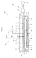
- FIG. 1 is an explanatory diagram illustrating the overall construction of the thin film formation apparatus according to the first embodiment of the present invention.
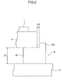
- Fig. 2 is an enlarged diagram illustrating a portion of the apparatus indicated by a reference character A in Fig. 1
- Fig. 3 is an enlarged diagram illustrating a portion of the apparatus indicated by a reference character B in Fig. 1.
- Fig. 4 is a diagram for explaining how to support an anode electrode
- Fig. 5 is a diagram for explaining how to support a cathode electrode.
- the thin film formation apparatus 100 includes a chamber (reaction chamber) 31, a gas introduction section 28 for introducing a reactant gas into the chamber 31, an evacuation section 29 for exhausting the reactant gas from the chamber 31, a planar anode electrode (first electrode) 4 and a planar cathode electrode (second electrode) 34 provided in the chamber 31, engagement members 6, 5 which respectively support the anode electrode 4 and the cathode electrode 34 in parallel relation, a high frequency power source 30 for applying high frequency power between the anode electrode 4 and the cathode electrode 34, and a sheath heater (heating section) 24 for heating the anode electrode 4.
- a substrate 1 to be formed with a film is placed on the anode electrode 4, and the anode electrode 4 and the cathode electrode 34 are supported movably in the direction of thermal expansion.
- the chamber 31 includes a main body 11 and a cover 10, which are each composed of a stainless steel, an aluminum alloy or the like.
- the cover 10 is fitted on the main body 11 with the intervention of an O-ring (not shown) or the like for sealing the chamber 31.
- the evacuation section 29, which includes an evacuation pipe 20, a pressure controller 22 and a vacuum pump 21, is connected to the chamber 31, so that the degree of the vacuum in the chamber 31 can be controlled at any desired level.
- the engagement member 6 includes four engagement members, which are provided on the bottom of the chamber 31 and respectively support the four corners of the anode electrode 4 thereon.
- the four engagement members 6 constitute the first support member.
- the anode electrode 4 is properly dimensioned according to the size of the substrate 1.
- the substrate 1 has a size of 900mm ⁇ 550mm to 1200mm ⁇ 750mm.
- the anode electrode 4 has a size of 1000mm ⁇ 600mm to 1200mm ⁇ 800mm.
- the anode electrode 4 may be composed of a stainless steel, an aluminum alloy, carbon or the like. In the first embodiment, the anode electrode 4 is composed of the aluminum alloy.
- the anode electrode 4 includes a sheath heater 24 incorporated therein. The temperature of the sheath heater 24 is controlled within the range between a room temperature and 600° C with the use of a temperature sensor of enclosed type such as a thermocouple 25.
- the anode electrode 4 is spaced from the chamber 31 by a distance D1 of 10mm to 30mm, as measured from the bottom of the chamber 31 to the lower surface of the anode electrode 4, by means of the engagement members 6.
- the engagement members 6 are each composed of a material, such as glass, alumina or zirconia, having a smaller heat conductivity. In the first embodiment, the engagement members 6 are each composed of zirconia.
- the anode electrode 4 has a smaller area in contact with the engagement members 6.
- the four engagement members 6 support only the four corners of the anode electrode 4 as described above.
- Surfaces of the engagement members 6 in contact with the anode electrode 4 each have an area of 30mm ⁇ 50mm.
- the anode supporting method and the contact area are determined so as not to allow the anode electrode 4 to warp.
- the surfaces of the engagement members 6 in contact with the anode electrode 4 are each formed with several recesses having a depth of 1mm to 5mm.
- the contact areas of the engagement members 6 can be reduced without reducing the strength of the engagement members 6.
- the engagement members 6 each include a support piece 6b which supports the lower surface of the anode electrode 4, and an engagement piece 6a which is horizontally spaced from the periphery of the anode electrode 4 supported on the support piece 6b.
- the engagement pieces 6a are dimensioned and positioned so as to be properly spaced from the periphery of the anode electrode 4.
- the engagement pieces 6a are spaced a distance D2 of 5mm from the periphery of the anode electrode 4 at a room temperature before the thermal expansion of the anode electrode 4.
- the anode electrode 4 is merely placed on the four engagement members 6 but not fixed by a screw or the like. Even if the anode electrode 4 is heated to be thermally expanded, the anode electrode 4 moves (slides) on the support pieces 6b of the engagement members 6 correspondingly to the thermal expansion. Thus, the thermal expansion is relieved.
- the anode electrode 4 is electrically connected to the chamber 31 via ground lines 26.
- the ground lines 26 each comprise an aluminum plate having a width of 10mm to 35mm and a thickness of 0.5mm to 3mm, and are fixed to the four corners of the anode electrode 4.
- the cathode electrode 34 includes a shower plate 2 and a rear plate 3, which are each composed of a stainless steel, an aluminum alloy or the like. In the first embodiment, the shower plate 2 and the rear plate 3 are each composed of the aluminum alloy.
- the cathode electrode 34 is properly dimensioned according to the size of the substrate 1. In the first embodiment, the cathode electrode 34 has a size of 1000mm ⁇ 600mm to 1200mm ⁇ 800mm.
- the cathode electrode 34 has a hollow inside, and is connected to the gas introduction section 28 via a reactant gas pipe 23. The reactant gas introduced into the cathode electrode 34 from the gas introduction section 28 via the reactant gas pipe 23 is ejected in a shower-like form from a plurality of through-holes formed in the shower plate 2 of the cathode electrode 34.
- the through-holes of the shower plate 2 preferably each have a diameter of 0.1mm to 2.0mm, and are arranged at a pitch of several millimeters to several centimeters.
- the engagement member 5 includes four engagement members which respectively support the four corners of the cathode electrode 34 thereon.
- the four engagement members 5 constitute the second support member.
- the engagement members 5 are respectively fixed to four support posts 8 each vertically extending from the bottom of the chamber 31 in the vicinity of upper ends of the support posts 8.
- a top plate 9 is fixed to the upper ends of the four support posts 8 for reinforcement of the support posts 8.
- the engagement members 5 constituting the second support member may each be composed of glass, alumina, zirconia or the like. In the first embodiment, the engagement members 5 are each composed of alumina or zirconia.
- the top plate 9 may be composed of a stainless steel, an aluminum alloy or the like. In the first embodiment, the top plate 9 is composed of the aluminum alloy.
- the cathode electrode 34 is also heated due to heat radiation from the anode electrode 4. As in the case of the engagement members 6, it is desirable that the cathode electrode 34 has the smallest possible area in contact with the engagement members 5. In the first embodiment, surfaces of the engagement members 5 in contact with the cathode electrode 34 each have an area of 100mm ⁇ 50mm. As in the case of the engagement members 6, the contact areas of the engagement members 5 are determined so as not to allow the cathode electrode 34 to warp.
- the engagement members 5 each include a support piece 5b which supports the lower surface of the cathode electrode 34, and an engagement piece 5a horizontally spaced from the periphery of the cathode electrode 34 supported on the support piece 5b.
- the engagement pieces 5a are dimensioned and positioned so as to be properly spaced from the periphery of the cathode electrode 34.
- the engagement pieces 5a are spaced a distance D3 of 5mm from the periphery of the cathode electrode 34 at a room temperature before the thermal expansion of the cathode electrode 34.
- the cathode electrode 34 is merely placed on the four engagement members 5 but not fixed by a screw or the like. Even if the cathode electrode 34 is heated to be thermally expanded, the cathode electrode 34 moves (slides) on the support pieces 5b of the engagement members 5 correspondingly to the thermal expansion. Thus, the thermal expansion is relieved.
- the anode electrode 4 and the cathode electrode 34 are each movable in the thermal expansion directions. Therefore, the anode electrode 4 and the cathode electrode 34 slide on the support pieces 6b, 5b of the engagement members 6, 5, whereby the thermal expansion thereof is relieved. Hence, the spacing between the anode electrode 4 and the cathode electrode 34 can be maintained within a designed spacing tolerance with no variation.
- the anode electrode 4 and the cathode electrode 34 can easily be removed from the apparatus in the maintenance of the apparatus, because the anode electrode 4 and the cathode electrode 34 are not fixed by screws or the like as described above. This facilitates the maintenance of the apparatus.
- the spacing D4 between the anode electrode 4 and the cathode electrode 34 is typically several millimeters to several tens millimeters. In the first embodiment, the spacing D4 is 2mm to 30mm.
- the tolerance of the spacing between the anode electrode 4 and the cathode electrode 34 is preferably several percent of a predetermined value. In the first embodiment, the spacing tolerance is within 1%.
- the high frequency power source 30, which includes a plasma excitation power source 12 and an impedance matching device 13, is connected to the cathode electrode 34 via a power inlet terminal 27, so that high frequency power is applied to the cathode electrode 34.
- the plasma excitation power source 12 typically employs a power output of 10W to 100KW at a frequency of DC to 108.48MHz. In the first embodiment, the plasma excitation power source 12 employs a power output of 10W to 100KW at a frequency of 13.56MHz to 54.24MHz.
- the reactant gas which contains SiH 4 diluted by H 2
- the reactant gas is introduced into the chamber 31 at a predetermined flow rate at a predetermined pressure through the cathode electrode 34, and the high frequency power is applied between the cathode electrode 34 and the anode electrode 4 to cause glow discharge.
- silicon is deposited on the substrate 1 for ten minutes, whereby a silicon thin film having a thickness of 300nm is formed on the substrate 1 with a film thickness variation of ⁇ 10%.
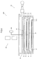
- the thin film formation apparatus 200 according to the second embodiment has a two stage structure which includes two sets of anode electrodes 4 and cathode electrodes 34, and two sets of engagement members 5 and engagement members 6. More specifically, the engagement members 6 for supporting the anode electrode 4 of the second stage are provided on the cathode electrode 34 of the first stage. Thus, the two sets of anode electrodes 4 and cathode electrodes 34 are stacked vertically.
- Support posts 8 supports the engagement members 5 of the first and second stages.
- the second embodiment provides the two stage structure, a three or more stage structure may be provided by repeating the aforesaid structure.
- the chamber 31, the gas introduction section 28, the evacuation section 29, the high frequency power source 30, the anode electrodes 4, the cathode electrodes 34, the engagement members 6 (first support member) and the engagement members 5 (second support member) respectively have the same constructions as those in the first embodiment.
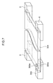
- FIG. 7 is a diagram for explaining how to support an anode electrode in the third embodiment
- Fig. 8 is a diagram for explaining how to support a cathode electrode in the third embodiment.
- one of the four corners of the anode electrode 304 is fixed at a single point by a engagement member 306, and one of the four corners of the cathode 334 is fixed at a single point by a engagement member 305 in the third embodiment.
- the other three corners of each of the anode electrode 304 and the cathode electrode 334 are supported on corresponding engagement members 6, 5 movably in thermal expansion directions as in the first embodiment.
- Cylindrical bosses 306a and 305a are provided upright on the engagement members 306 and 305, respectively.
- a hole 304a is formed in the one of the corners of the anode electrode 304 in association with the boss 306a, and a hole 334a is formed in the one of the corners of the cathode electrode 334 in association with the boss 305a.
- the bosses 306a and 305a of the engagement members 306 and 305 are respectively fitted in the holes 304a and 334a of the anode electrode 304 and the cathode electrode 334, whereby the anode electrode 304 and the cathode electrode 334 are detachably fixed to the engagement members 306 and 305, respectively.
- the positions of the anode electrode 304 and the cathode electrode 334 are naturally determined by the engagement members 306, 305, respectively, so that the anode electrode 304 and the cathode electrode 334 can easily be positioned. Since the anode electrode 304 and the cathode electrode 334 are each fixed at one corner thereof to the engagement member 306, 305, the other three corners thereof are freely movable in the thermal expansion direction.
- the spacing between the anode electrode 304 and the cathode electrode 334 can accurately be maintained as in the first embodiment.
- the engagement members 306, 305 may be composed of the same material as the engagement members 6, 5.
- the thin film formation apparatus according to the third embodiment has substantially the same construction as that of the first embodiment except for the aforesaid point. Though not shown, the thin film formation apparatus according to the third embodiment may be modified as having a multi-stage structure which includes plural pairs of anode electrodes and cathode electrodes stacked in a single chamber and plural sets of engagement members as in the second embodiment.
- the first and second support members support the first and second electrodes in parallel relation, and at least one of the first and second electrodes is movable in the thermal expansion direction. Therefore, when the first and second electrodes are heated to be thermally expanded, the at least one electrode moves in the thermal expansion direction, whereby the thermal expansion can be relieved. As a result, the variation in the spacing between the first and second electrodes is reduced, so that the performance of the apparatus is improved.
Landscapes
- Chemical & Material Sciences (AREA)
- Engineering & Computer Science (AREA)
- Physics & Mathematics (AREA)
- Plasma & Fusion (AREA)
- Analytical Chemistry (AREA)
- Chemical Kinetics & Catalysis (AREA)
- General Chemical & Material Sciences (AREA)
- Materials Engineering (AREA)
- Mechanical Engineering (AREA)
- Metallurgy (AREA)
- Organic Chemistry (AREA)
- Chemical Vapour Deposition (AREA)
- Photovoltaic Devices (AREA)
Abstract
Description
Claims (14)
- A thin film formation apparatus for forming a thin film on a substrate, comprising:wherein the substrate is placed on the heated electrode, and at least one of the first and second electrodes is supported movably in a direction of thermal expansion by the corresponding support member.a reaction chamber;a gas introduction section for introducing a reactant gas into the reaction chamber;an evacuation section for exhausting the reactant gas from the reaction chamber;first and second planar electrodes provided in the reaction chamber;first and second support members which respectively support the first and second electrodes in parallel relation;a high frequency power source for applying high frequency power between the first and second electrodes; anda heating section for heating one of the first and second electrodes;
- A thin film formation apparatus as set forth in claim 1, wherein the at least one of the first and second electrodes is partly fixed to the corresponding support member.
- A thin film formation apparatus as set forth in claim 1, wherein a portion of the at least one of the first and second electrodes is fixed to the corresponding support member, and the other portion of the at least one electrode is supported movably in the thermal expansion direction by the corresponding support member.
- A thin film formation apparatus as set forth in claim 1, wherein the first and second electrodes are supported horizontally and perpendicularly to a gravity direction by the first and second support members.
- A thin film formation apparatus as set forth in claim 4,
wherein the first and second support members each include a plurality of engagement members which are loosely engaged with a periphery of the corresponding electrode,
the engagement members each including an engagement piece spaced horizontally from the periphery of the electrode, and a support piece which supports a lower surface of the electrode. - A thin film formation apparatus as set forth in claim 4,
wherein the first and second electrodes are generally rectangular,
the first and second support members each including four engagement members which support four corners of the corresponding electrode. - A thin film formation apparatus as set forth in claim 1, wherein the first and second support members are each composed of an insulative material.
- A thin film formation apparatus as set forth in claim 7,
wherein the insulative material is one of glass, alumina and zirconia. - A thin film formation apparatus for forming thin films on substrates respectively, comprising:wherein each substrate is placed on the heated electrode in each of the pairs, and at least one of the first and second electrodes in each of the pairs is supported movably in a direction of thermal expansion by the corresponding support member.a reaction chamber;a gas introduction section for introducing a reactant gas into the reaction chamber;an evacuation section for exhausting the reactant gas from the reaction chamber;plural pairs of first and second planar electrodes provided in the reaction chamber;first and second support members which respectively support the first and second electrodes in each of the pairs in parallel relation;a high frequency power source for applying high frequency power between the first and second electrodes in each of the pairs; anda heating section for heating one of the first and second electrodes in each of the pairs;
- A thin film formation apparatus as set forth in claim 9, wherein at least one of the first and second electrodes in each of the pairs is partly fixed to the corresponding support member.
- A thin film formation apparatus as set forth in claim 9, wherein a portion of at least one of the first and second electrodes in each of the pairs is fixed to the corresponding support member, and the other portion of the at least one electrode is supported movably in the thermal expansion direction by the corresponding support member.
- A thin film formation apparatus as set forth in claim 9, wherein the plural pairs of the first and second electrodes are supported horizontally and perpendicularly to a gravity direction by the first and second support members.
- A thin film formation method which employs a thin film formation apparatus as set forth in claim 1 for forming a thin film on a substrate, the method comprising the steps of:placing the substrate on the heated electrode;supplying a reactant gas into the reaction chamber; andapplying high frequency power between the first and second electrodes.
- A thin film formation method which employs a thin film formation apparatus as set forth in claim 9 for forming thin films on substrates respectively, the method comprising the steps of:placing each substrate on the heated electrode in each of the pairs;supplying a reactant gas into the reaction chamber;applying high frequency power between the first and second electrodes in each of the pairs.
Applications Claiming Priority (2)
| Application Number | Priority Date | Filing Date | Title |
|---|---|---|---|
| JP2002299069 | 2002-10-11 | ||
| JP2002299069 | 2002-10-11 |
Publications (3)
| Publication Number | Publication Date |
|---|---|
| EP1420081A2 true EP1420081A2 (en) | 2004-05-19 |
| EP1420081A3 EP1420081A3 (en) | 2006-05-03 |
| EP1420081B1 EP1420081B1 (en) | 2010-12-15 |
Family
ID=32064229
Family Applications (1)
| Application Number | Title | Priority Date | Filing Date |
|---|---|---|---|
| EP03022925A Expired - Lifetime EP1420081B1 (en) | 2002-10-11 | 2003-10-09 | Thin film formation apparatus and thin film formation method employing the apparatus |
Country Status (3)
| Country | Link |
|---|---|
| US (1) | US7032536B2 (en) |
| EP (1) | EP1420081B1 (en) |
| DE (1) | DE60335337D1 (en) |
Cited By (2)
| Publication number | Priority date | Publication date | Assignee | Title |
|---|---|---|---|---|
| WO2007060876A1 (en) | 2005-11-25 | 2007-05-31 | Sharp Kabushiki Kaisha | Plasma processing apparatus and plasma processing method |
| US7741144B2 (en) | 2007-11-02 | 2010-06-22 | Applied Materials, Inc. | Plasma treatment between deposition processes |
Families Citing this family (16)
| Publication number | Priority date | Publication date | Assignee | Title |
|---|---|---|---|---|
| US20050277302A1 (en) * | 2004-05-28 | 2005-12-15 | Nguyen Son V | Advanced low dielectric constant barrier layers |
| JP4659820B2 (en) * | 2005-03-07 | 2011-03-30 | シャープ株式会社 | Plasma processing apparatus and semiconductor thin film manufacturing method using the same |
| EP2037721A1 (en) * | 2006-06-23 | 2009-03-18 | Sharp Kabushiki Kaisha | Plasma processing apparatus, plasma processing method and photoelectric conversion element |
| US8203071B2 (en) | 2007-01-18 | 2012-06-19 | Applied Materials, Inc. | Multi-junction solar cells and methods and apparatuses for forming the same |
| KR100924287B1 (en) * | 2007-05-10 | 2009-10-30 | 한국과학기술연구원 | DC power plasma deposition apparatus that does not have a positive pole, the material deposition method without the positive pole and the diamond thin film produced thereby |
| US20090130827A1 (en) * | 2007-11-02 | 2009-05-21 | Soo Young Choi | Intrinsic amorphous silicon layer |
| WO2011146571A2 (en) * | 2010-05-21 | 2011-11-24 | Applied Materials, Inc. | Tightly-fitted ceramic insulator on large-area electrode |
| EP2453472A1 (en) * | 2010-11-16 | 2012-05-16 | Applied Materials, Inc. | Pallet For High Temperature Processing |
| KR101760316B1 (en) * | 2015-09-11 | 2017-07-21 | 주식회사 유진테크 | Substrate Processing Apparatus |
| CN114666965B (en) | 2017-06-27 | 2025-08-01 | 佳能安内华股份有限公司 | Plasma processing apparatus |
| PL3648554T3 (en) | 2017-06-27 | 2021-11-22 | Canon Anelva Corporation | PLASMA PROCESSING DEVICE |
| EP4017223B1 (en) | 2017-06-27 | 2025-10-15 | Canon Anelva Corporation | Plasma processing apparatus |
| EP3648550B1 (en) | 2017-06-27 | 2021-06-02 | Canon Anelva Corporation | Plasma treatment device |
| PL3817517T3 (en) * | 2018-06-26 | 2024-10-28 | Canon Anelva Corporation | Plasma treatment device, plasma treatment method, program, and memory medium |
| DE102018133007A1 (en) * | 2018-12-20 | 2020-06-25 | Bayerische Motoren Werke Aktiengesellschaft | Method for producing a high-voltage battery |
| WO2021109425A1 (en) * | 2019-12-04 | 2021-06-10 | 江苏菲沃泰纳米科技有限公司 | Coating equipment |
Family Cites Families (12)
| Publication number | Priority date | Publication date | Assignee | Title |
|---|---|---|---|---|
| JPS5933251B2 (en) * | 1977-10-19 | 1984-08-14 | 株式会社日立製作所 | Plasma vapor phase processing equipment |
| US4264393A (en) | 1977-10-31 | 1981-04-28 | Motorola, Inc. | Reactor apparatus for plasma etching or deposition |
| US4885074A (en) * | 1987-02-24 | 1989-12-05 | International Business Machines Corporation | Plasma reactor having segmented electrodes |
| JPH04326725A (en) * | 1991-04-26 | 1992-11-16 | Tokyo Electron Ltd | Plasma apparatus |
| JP3146112B2 (en) * | 1993-12-24 | 2001-03-12 | シャープ株式会社 | Plasma CVD equipment |
| JPH08288096A (en) * | 1995-02-13 | 1996-11-01 | Mitsubishi Electric Corp | Plasma processing device |
| JP3238082B2 (en) * | 1996-05-16 | 2001-12-10 | シャープ株式会社 | Electronic device manufacturing equipment |
| JP3940190B2 (en) * | 1996-09-30 | 2007-07-04 | 松下電器産業株式会社 | Vacuum processing equipment |
| JP3598717B2 (en) * | 1997-03-19 | 2004-12-08 | 株式会社日立製作所 | Plasma processing equipment |
| JP3544136B2 (en) * | 1998-02-26 | 2004-07-21 | キヤノン株式会社 | Plasma processing apparatus and plasma processing method |
| JP2961103B1 (en) * | 1998-04-28 | 1999-10-12 | 三菱重工業株式会社 | Plasma chemical vapor deposition equipment |
| US6377437B1 (en) * | 1999-12-22 | 2002-04-23 | Lam Research Corporation | High temperature electrostatic chuck |
-
2003
- 2003-10-08 US US10/680,213 patent/US7032536B2/en not_active Expired - Fee Related
- 2003-10-09 DE DE60335337T patent/DE60335337D1/en not_active Expired - Lifetime
- 2003-10-09 EP EP03022925A patent/EP1420081B1/en not_active Expired - Lifetime
Cited By (4)
| Publication number | Priority date | Publication date | Assignee | Title |
|---|---|---|---|---|
| WO2007060876A1 (en) | 2005-11-25 | 2007-05-31 | Sharp Kabushiki Kaisha | Plasma processing apparatus and plasma processing method |
| EP1959480A4 (en) * | 2005-11-25 | 2010-04-21 | Sharp Kk | Plasma processing apparatus and plasma processing method |
| US8093142B2 (en) | 2005-11-25 | 2012-01-10 | Sharp Kabushiki Kaisha | Plasma processing apparatus and plasma processing method |
| US7741144B2 (en) | 2007-11-02 | 2010-06-22 | Applied Materials, Inc. | Plasma treatment between deposition processes |
Also Published As
| Publication number | Publication date |
|---|---|
| US7032536B2 (en) | 2006-04-25 |
| EP1420081A3 (en) | 2006-05-03 |
| DE60335337D1 (en) | 2011-01-27 |
| EP1420081B1 (en) | 2010-12-15 |
| US20040069230A1 (en) | 2004-04-15 |
Similar Documents
| Publication | Publication Date | Title |
|---|---|---|
| EP1420081B1 (en) | Thin film formation apparatus and thin film formation method employing the apparatus | |
| JP4185483B2 (en) | Plasma processing equipment | |
| JP3338884B2 (en) | Semiconductor processing equipment | |
| JP3970815B2 (en) | Semiconductor device manufacturing equipment | |
| JP4936297B2 (en) | Plasma processing apparatus, plasma processing method, and semiconductor device | |
| US20100277050A1 (en) | Plasma processing apparatus | |
| CN107810542A (en) | Peripheral plasma processing unit with Forming Workpiece fixture | |
| US8093142B2 (en) | Plasma processing apparatus and plasma processing method | |
| JP4421864B2 (en) | Thin film manufacturing apparatus and thin film manufacturing method using the apparatus | |
| EP1858061B1 (en) | Plasma treatment apparatus and semiconductor thin film manufacturing method using same | |
| JP5053595B2 (en) | DLC film forming method and DLC film manufacturing apparatus | |
| US6846521B2 (en) | Apparatus and method for forming deposited film | |
| KR20100008052A (en) | Chemical vapor deposition apparatus | |
| JP4290207B2 (en) | Semiconductor element manufacturing apparatus and semiconductor element manufacturing method | |
| CN117358713A (en) | Cleaning device and cleaning method for process substrate carrier | |
| JP2010219344A (en) | Plasma processing apparatus | |
| KR20090073271A (en) | Substrate processing chamber with capacitively coupled electrodes with laser beam |
Legal Events
| Date | Code | Title | Description |
|---|---|---|---|
| PUAI | Public reference made under article 153(3) epc to a published international application that has entered the european phase |
Free format text: ORIGINAL CODE: 0009012 |
|
| AK | Designated contracting states |
Kind code of ref document: A2 Designated state(s): AT BE BG CH CY CZ DE DK EE ES FI FR GB GR HU IE IT LI LU MC NL PT RO SE SI SK TR |
|
| AX | Request for extension of the european patent |
Extension state: AL LT LV MK |
|
| PUAL | Search report despatched |
Free format text: ORIGINAL CODE: 0009013 |
|
| AK | Designated contracting states |
Kind code of ref document: A3 Designated state(s): AT BE BG CH CY CZ DE DK EE ES FI FR GB GR HU IE IT LI LU MC NL PT RO SE SI SK TR |
|
| AX | Request for extension of the european patent |
Extension state: AL LT LV MK |
|
| 17P | Request for examination filed |
Effective date: 20060922 |
|
| 17Q | First examination report despatched |
Effective date: 20061113 |
|
| AKX | Designation fees paid |
Designated state(s): DE FR |
|
| GRAP | Despatch of communication of intention to grant a patent |
Free format text: ORIGINAL CODE: EPIDOSNIGR1 |
|
| GRAS | Grant fee paid |
Free format text: ORIGINAL CODE: EPIDOSNIGR3 |
|
| GRAA | (expected) grant |
Free format text: ORIGINAL CODE: 0009210 |
|
| AK | Designated contracting states |
Kind code of ref document: B1 Designated state(s): DE FR |
|
| REF | Corresponds to: |
Ref document number: 60335337 Country of ref document: DE Date of ref document: 20110127 Kind code of ref document: P |
|
| PLBE | No opposition filed within time limit |
Free format text: ORIGINAL CODE: 0009261 |
|
| STAA | Information on the status of an ep patent application or granted ep patent |
Free format text: STATUS: NO OPPOSITION FILED WITHIN TIME LIMIT |
|
| 26N | No opposition filed |
Effective date: 20110916 |
|
| REG | Reference to a national code |
Ref country code: DE Ref legal event code: R097 Ref document number: 60335337 Country of ref document: DE Effective date: 20110916 |
|
| PGFP | Annual fee paid to national office [announced via postgrant information from national office to epo] |
Ref country code: FR Payment date: 20121018 Year of fee payment: 10 Ref country code: DE Payment date: 20121003 Year of fee payment: 10 |
|
| REG | Reference to a national code |
Ref country code: DE Ref legal event code: R119 Ref document number: 60335337 Country of ref document: DE Effective date: 20140501 |
|
| REG | Reference to a national code |
Ref country code: FR Ref legal event code: ST Effective date: 20140630 |
|
| PG25 | Lapsed in a contracting state [announced via postgrant information from national office to epo] |
Ref country code: FR Free format text: LAPSE BECAUSE OF NON-PAYMENT OF DUE FEES Effective date: 20131031 Ref country code: DE Free format text: LAPSE BECAUSE OF NON-PAYMENT OF DUE FEES Effective date: 20140501 |