BACKGROUND OF THE INVENTION
(a) Field of the Invention
The present invention relates to a drive apparatus and method for a
plasma display panel. More particularly, the present invention relates to a drive
apparatus and method for a plasma display panel in which the drive apparatus
and method improve contrast and prevent mis-discharge.
(b) Description of the Related Art
Flat display devices such as the liquid crystal display (LCD), the field
emission display (FED), and the plasma display panel (PDP) have recently
been undergoing rapid development. The PDP has some advantages over the
other flat display configurations, such as in higher brightness, better illumination
efficiency, and a wider viewing angle. Accordingly, many anticipate the PDP to
replace the cathode ray tube (CRT) for displays having screen sizes of 40
inches or greater.
The PDP is a display device that utilizes plasma generated by gas
discharge to realize the display of characters or images. The PDP includes a
configuration in which many hundreds to many thousands of pixels (depending
on the size of the PDP) are arranged in a matrix. PDPs are classified into the
two different types of the DC PDP and AC PDP depending on the drive voltage
waveform and discharge cell structure.
In the DC PDP, electrodes are fully exposed in a discharge space such
that current flows in the discharge space while voltage is being applied. As a
result, resistance for limiting the flow of current must be provided. On the other
hand, in the AC PDP, the electrodes are covered with a dielectric layer such
that current is limited through the formation of a natural capacitance. As a result,
the electrodes are protected from the collision of ions so that the AC PDP has a
longer life span.
(1) Elimination interval
After a final sustain discharge is completed, a (+) electric charge and a
(-) electric charge are accumulated respectively in the X electrodes and the Y
electrodes.
Following the completion of the sustain discharge, an elimination ramp
voltage that gently increases from 0V to +Ve(V) is applied to the X electrodes.
Accordingly, a wall charge formed in the X electrodes and the Y electrodes is
gradually eliminated.
(2) Y ramp ascending interval
In the Y ramp ascending interval, the address electrodes and the X
electrodes are maintained at 0V, and a ramp voltage gently increasing from
voltage Vs to voltage Vset is applied to the Y electrodes. While the ramp
voltage is increasing, a first weak reset discharge occurs from the Y electrodes
to the address electrodes and to the X electrodes in all discharge cells. As a
result, a (-) wall charge is accumulated in the Y electrodes, and a (+) wall
charge is accumulated in the address electrodes and the X electrodes.
(3) Y ramp descending interval
In a second half of the reset interval and in a state where the X
electrodes are maintained at a constant voltage Ve, a ramp voltage gently
decreasing from voltage Vs to 0V is applied to the Y electrodes. While this
ramp voltage is decreasing, a second weak reset discharge occurs, again in all
the discharge cells.
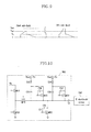
According to the conventional reset method shown in FIG. 3, the reset
discharge occurs in the Y ramp ascending interval and the Y ramp descending
interval such that the amount of wall discharge in the cells is adjusted.
Accordingly, a precise addressing operation occurs in a subsequent address
interval. At this time, the larger the voltage difference between the Y electrodes
and the X electrodes, the greater the precision in the addressing operation in
the subsequent addressing interval.
However, with the conventional reset method shown in FIG. 3, Vset,
which is a high voltage of approximately 380V, is applied to the Y electrodes,
while the ground voltage is supplied to the X electrodes. Therefore, an
unnecessarily high voltage is applied between the X electrodes and the Y
electrodes such that a strong discharge occurs, thereby deteriorating the
contrast of the PDP.
SUMMARY OF THE INVENTION
It is one object of the present invention to provide a drive apparatus and
method for a plasma display panel, in which the drive apparatus and method
prevent unnecessary discharge in a reset interval to improve contrast and that
prevent mis-discharge.
In one embodiment, the present invention provides a drive method for a
plasma display panel that includes first electrodes, second electrodes, and
panel capacitors formed between the first and second electrodes. The method
includes during a reset interval (a) applying a voltage having a waveform
increasing from a first voltage to a second voltage to the first electrodes during
a first interval; and (b) floating a voltage of the second electrodes during a
portion of the first interval thereby increasing the voltage of the second
electrodes from a third voltage to a fourth voltage responsive to the voltage
applied to the first electrodes and to a voltage of both sides of a panel
capacitor,.
In another aspect, the present invention provides a drive method for a
plasma display panel that includes first electrodes, second electrodes, and
panel capacitors formed between the first and second electrodes. The method
includes (a) applying predetermined voltages to the first and second electrodes
so that a first voltage difference develops therebetween, the application of
these voltages occurring during a reset interval of a first sub-field; and (b)
applying predetermined voltages to the first and second electrodes so that a
second voltage difference that is greater than the first voltage difference
develops between the first and second electrodes, the application of these
voltages occurring during a reset interval of a second sub-field, in which the
second sub-field exhibits a higher gray than the first sub-field.
In yet another aspect, the present invention provides a drive method for
a plasma display panel that includes scan electrodes, common electrodes, and
panel capacitors formed between the first and second electrodes. The method
includes, in a reset interval of a first sub-field, (a) applying a voltage having an
increasing ramp waveform to the scan electrodes, during a first interval; and (b)
floating the common electrodes during a portion of the first interval such that a
voltage of the common electrodes increases to a first voltage, which
corresponds to a voltage applied to the scan electrodes and to a voltage
applied to both sides of the panel capacitor; and, in a reset interval of a second
sub-field, which exhibits a higher gray than the first sub-field, (c) applying a
voltage having an increasing ramp waveform to the scan electrodes, during a
second interval; and (d) floating the common electrodes during a portion of the
second interval such that the voltage of the common electrodes increases to a
second voltage, which is a smaller voltage than the first voltage.
The present invention also provides a drive apparatus for a plasma
display panel that includes scan electrodes, common electrodes, and panel
capacitors provided between the scan electrodes and the common electrodes.
The apparatus includes a first transistor coupled to the scan electrode and
applying a voltage of an increasing ramp waveform to the scan electrode during
a first interval; a second transistor coupled to the scan electrode and applying a
voltage of a decreasing ramp waveform to the scan electrode during a second
interval; and a third transistor coupled between the common electrode and a
first voltage. The third transistor floats the common electrode during a portion of
the first interval such that a voltage of the common electrode is increased from
a second voltage to a third voltage responsive to the voltage applied to the scan
electrode and a voltage to both sides of the panel capacitor.
In another aspect, the present invention provides a drive apparatus for
a plasma display panel that includes scan electrodes, common electrodes, and
panel capacitors provided between the scan electrodes and the common
electrodes, the driving field of the plasma display being divided into a plurality of
sub-fields. The apparatus includes a first transistor coupled to the scan
electrode and to apply a voltage thereto of a ramp waveform that increases
from a first voltage to a second voltage, the voltage being applied during a reset
interval of a first sub-field; a second transistor coupled to the scan electrode
and applying a voltage thereto of a ramp waveform that increases from the first
voltage to a third voltage, which is greater than the second voltage, the voltage
being applied during a reset interval of a second sub-field, which exhibits a
higher gray than the first sub-field; and a third transistor coupled to the scan
electrode and applying a voltage thereto of a decreasing ramp waveform.
BRIEF DESCRIPTION OF THE DRAWINGS
The accompanying drawings, which are incorporated in and constitute
a part of the specification, illustrate an embodiment of the invention, and,
together with the description, serve to explain the principles of the invention:
DETAILED DESCRIPTION OF THE PREFERRED EMBODIMENTS
Preferred embodiments of the present invention will now be described
in detail with reference to the accompanying drawings.
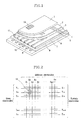
FIG. 4 is a drawing showing a plasma display panel according to a
preferred embodiment of the present invention.
With reference to FIG. 4, a plasma display panel (PDP) according to a
preferred embodiment of the present invention includes a plasma panel 100, an
address driver 200, a Y electrode driver 320, an X electrode driver 340, and a
controller 400. The plasma panel 100 includes a plurality of address electrodes
(A1∼Am) that are arranged in a column direction, and scan electrodes (Y
electrodes) (Y1∼Yn) and common electrodes (X electrodes) (X1∼Xn)
arranged alternately in a row direction.
The address driver 200 receives address drive control signals SA from
the controller 400, and applies display data signals to each of the address
electrodes to select discharge cells that will perform display. The Y electrode
driver 320 and the X electrode driver 340 receive from the controller 400 Y
electrode drive signals SY and X electrode drive signals SX, respectively, for
application of the same respectively to the X electrodes and the Y electrodes.
The controller 400 receives external image signals and generates the
address drive signals SA, the Y electrode drive signals SY, and the X electrode
drive signals SX. The controller 400 then transmits these signals to the address
driver 200, the Y electrode driver 320, and the X electrode driver 340.
FIG. 5 is a drive waveform of a plasma display panel according to a first
preferred embodiment of the present invention. In the drawing, X, Y, and A
indicate voltage waveforms of voltages applied to the X electrodes, the Y
electrodes, and the address electrodes, respectively.
Operations in a reset interval according to the first preferred
embodiment of the present invention will now be described in detail with
reference to FIG. 5.
(1) Elimination interval (t1 ∼ t2)
A voltage applied to the X electrodes is steadily increased from 0V to a
first voltage Ve (for example, 190V). Also, 0V are applied to the Y electrodes
(Y1, ..., Yn) and the address electrodes (A1, ..., Am). Accordingly, a weak
discharge occurs between the X electrodes and Y electrodes, and between the
X electrodes and address electrodes, and a negative wall charge is formed in
the peripheries of the X electrodes.
(2) Y ramp ascending interval (t3 ∼ t4)
A voltage applied to the Y electrodes is steadily increased from a
second voltage Vs, which is slightly lower than the first voltage Ve (for example,
180V), to a third voltage Vset, which is significantly higher than the first voltage
Ve (for example, 400V). 0V are applied to the address electrodes during this
time.
Also, during an interval from a specific point of the Y ramp ascending
interval to an end of the Y ramp ascending interval (tF ∼ t4), a voltage is
applied to the X electrodes that steadily increases to a fourth voltage VFB.
Optimal values for the interval (tF ∼ t4) and the fourth voltage VFB may be
established through repeated experimentation. This increasing voltage may be
directly received from the X electrode driver 340. However, as will be described
hereinafter, all outputs of the X electrode driver 340 come to be in an
electrically floating state (i.e., high impedance state) such that the same effect
is obtained.
(3) Y ramp descending interval (t5 ∼ t7)
The X electrodes (X1, ..., Xn) are maintained at the first voltage Ve, and
the voltage applied to the Y electrodes steadily decreases from the second
voltage Vs to 0V. Further, 0V are applied to the address electrodes.
In such a drive waveform of the first preferred embodiment of the
present invention, with the application of an increasing voltage to the X
electrodes in a latter-half portion (tF ∼ t4) of the Y ramp ascending interval, an
important advantage is realized. That is, in the Y ramp ascending interval (t3 ∼
t4), a voltage smaller than that of the prior art is applied between the Y
electrodes and the X electrodes such that an unnecessarily strong discharge
generated between the Y electrodes and the X electrodes is reduced, thereby
improving contrast of the PDP.
FIG. 6 is a detailed circuit diagram of the Y electrode driver 320 and the
X electrode driver 340 according to the first preferred embodiment of the
present invention, and FIG. 7 is a switching timing diagram of the circuit shown
in FIG. 6.
In the Y electrode driver 320 of the first preferred embodiment of the
present invention, transistors M1 and M2 are coupled in series between the
second voltage (Vs), which is a sustain discharge voltage, and the ground
voltage. Also, a transistor M3 is coupled to a common node between the
transistors M1 and M2 and to a first terminal of a panel capacitor Cp (i.e., Y
electrodes) (the panel capacitor exhibits an equivalent capacitance between the
X electrodes and the Y electrodes). A first terminal of a capacitor C1 is coupled
to the common node between the transistors M1 and M2, and a diode D1 is
coupled between a voltage Vset-Vs and a second terminal of the capacitor C1.
In addition, a transistor M4 is provided between the first terminal of the
panel capacitor Cp and the capacitor C1 to apply the ascending ramp voltage to
the Y electrodes, and a transistor M5 is provided between the first terminal of
the panel capacitor C1 and the ground voltage to apply the descending ramp
voltage to the Y electrodes. To supply a constant current between sources and
drains of the transistors M4 and M5, capacitors C2 and C3 are provided
between the drain and gate of the transistor M4 and the drain and gate of the
transistor M5, respectively.
With respect to the X electrode driver 340 of the first preferred
embodiment of the present invention, a transistor M8 is provided between the
first voltage Ve and a second terminal of the panel capacitor Cp (i.e., X
electrodes), and a transistor M7 is provided between the second terminal of the
panel capacitor Cp and ground. The transistor M7 is floated between the
second terminal of the panel capacitor Cp and ground to create a high
impedance, thereby realizing the application of an increasing voltage to the X
electrodes in the Y ramp ascending interval as described with reference to FIG.
5.
Further, a transistor M6 is provided between the first voltage Ve and the
second terminal of the panel capacitor Cp to apply an elimination waveform to
the X electrodes. A capacitor C4 is provided between a drain and a gate of the
transistor M6 so that a constant current flows between a source and the drain
of the transistor M6.
A drive method according to a first preferred embodiment of the present
invention will now be described with reference to FIGS. 5, 6, and 7.
It is assumed that the voltage Vset-Vs is charged in the capacitor C1.
Such charging is easily realized by controlling the transistor M2 or the transistor
M5 to On. At t=t1 in FIG. 7, the transistor M6 is controlled On in a state where
the transistors M2 and M3 are On. Accordingly, since a constant current is
supplied to the second terminal of the panel capacitor Cp (X electrodes), an
elimination ramp voltage that increases from 0V to the first voltage Ve is
applied to the X electrodes as shown in FIG. 5.
Next, at t=t2, the transistor M6 is controlled to Off and the transistor M7
is controlled to On. As a result, the voltage of the second terminal of the panel
capacitor Cp (X electrodes) becomes 0V.
At t=t3, in a state where the transistor M7 is On, the transistors M2 and
M3 are controlled to Off and the transistors M1 and M4 are controlled to On.
Therefore, the second voltage Vs is supplied to the first terminal of the
capacitor C1, and because the voltage Vset-Vs is already charged in the
capacitor C1, the voltage of the second terminal of the capacitor C1 becomes
Vset. Further, the voltage Vset of the second terminal of the capacitor C1 is
supplied to the first terminal of the panel capacitor (Y electrodes) through the
transistor M4. At this time, since a constant current flows between the source
and drain of the transistor M4 by the influence of the capacitor C2, a voltage
that increases from the second voltage Vs to the third voltage Vset is applied to
the first terminal of the capacitor Cp (Y electrodes).
In addition, the transistor M7 is controlled to Off at a specific point (t=tF)
of the interval (t3∼t4) when the voltage of the first terminal of the panel
capacitor Cp (Y electrodes) increases from the second voltage Vs to the third
voltage Vset. Accordingly, the second terminal of the panel capacitor Cp (X
electrodes) that is maintained at 0V changes to a floating state such that the
voltage of the second terminal of the panel capacitor Cp (X electrodes)
(hereinafter referred to as a floating voltage" ) varies in accordance with the
voltage of the first terminal (Y electrodes) as shown in FIG. 5.
In more detail, the voltage of the second terminal of the panel capacitor
Cp (X electrodes) corresponds to a value of subtracting the voltage charged in
the panel capacitor Cp from the voltage of the Y electrodes such that the
voltage of the X electrodes increases from 0V to the fourth voltage VFB and
following the same increasing pattern of the voltage of the Y electrodes
increases. At this time, the floating voltage VFB is determined according to the
interval of floating the second terminal of the panel capacitor Cp (X electrodes)
(i.e., the interval when the transistor M7 is controlled to Off). Hence, the greater
the floating interval, the higher the floating voltage VFB. Therefore, in the
preferred embodiment of the present invention, determining the optimal floating
voltage VFB through repeated experimentation is, in effect, determining the
point at which the transistor M7 is controlled to Off.
At t=t4, the transistors M3 and M7 are controlled to On, and the
transistor M4 is controlled to Off. Accordingly, the second voltage Vs is applied
to the Y electrodes, and the ground voltage is applied to the X electrodes. At
t=t5, the transistor M7 is controlled to Off, the transistor M8 is controlled to On,
and the voltage Ve is applied to the X electrodes. At t=t6, in a state where the
transistor M3 is controlled to On, the transistor M1 is controlled to Off and the
transistor M5 is controlled to On. As a result, the voltage of the first terminal of
the panel capacitor Cp (Y electrodes) decreases from the second voltage Vs to
the ground voltage.
In the reset drive method of the first preferred embodiment of the
present invention described above, during a portion of the Y ramp ascending
interval (t3 ∼ t4), the X electrodes are floated and a corresponding floating
voltage is applied to the X electrodes thereby reducing a difference in voltages
applied to the X electrodes and the Y electrodes. Therefore, the contrast of the
PDP is improved.
However, with the drive method of the first preferred embodiment of the
present invention, reset is unreliable so that a subsequent addressing operation
without flaws cannot be obtained. Accordingly, the following problems result if,
in order to improve contrast, floating voltages of the same magnitude are
applied to the X electrodes with respect to all the sub-fields.
In particular, if the X electrodes are driven by floating the same as in
the first preferred embodiment of the present invention, reset is unstable such
that discharge occurs in pixels where discharge should not occur during a
subsequent sustain discharge interval. Such mis-discharge caused by unstable
reset is a significantly greater problem in high gray sub-fields (sub-fields where
there are many sustain discharge pulses) than in low gray sub-fields (sub-fields
where there are few sustain discharge pulses).
In second and third preferred embodiments of the present invention,
the difference in voltages between the X electrodes and Y electrodes is
differently set according to sub-field to thereby improve contrast and reduce
mis-discharge.
FIG. 8 is a drive waveform of a plasma display panel according to a
second preferred embodiment of the present invention.
As shown in the drawing, in a drive method according to the second
preferred embodiment of the present invention, a floating voltage VFB1 of the X
electrodes applied during the reset interval of a low gray sub-field (a first sub-field)
is greater than a floating voltage VFB2 applied during the reset interval of
a high gray sub-field (an nth sub-field). In the Fig. 8, a first sub-field and an nth
sub-field are represented as examples of low gray sub-field and high gray sub-field,
respectively.
Therefore, the floating voltage VFB1 of the X electrodes is established
at a high level (i.e., a low voltage difference between the Y electrodes and the X
electrodes) during the reset interval of the low gray sub-field during which a
relatively minimal influence of mis-discharge is received such that discharge
during the reset interval is reduced. The result of this is that contrast is
increased. Further, during the reset interval of the high gray sub-field (the sub-field
where there are many sustain discharge pulses) during which the affect of
mis-discharge is significant, the floating voltage VFB2 of the X electrodes is
established at a low level (i.e., a high voltage difference between the Y
electrodes and the X electrodes) to thereby enable reliable reset. This prevents
mis-discharge during a subsequent sustain discharge interval.
The drive method according to the second preferred embodiment of the
present invention, the drive waveform for which is shown in FIG. 8, may be
realized using the drive circuit of FIG. 6.
In more detail, an interval tFB1 that floats the transistor M7 during the
reset interval of the low gray sub-field is longer than an interval tFB2 that floats
the transistor during the reset interval of the high gray sub-field. Therefore, the
floating voltage VFB1 applied to the X electrodes is higher than the floating
voltage VFB2 applied to the X electrodes of the reset interval of the high gray
sub-field.
FIG. 9 is a drive waveform of a plasma display panel according to a
third preferred embodiment of the present invention.
As shown in the drawing, in a drive method according to the third
preferred embodiment of the present invention, a voltage Vset1 of the Y
electrodes applied during a reset interval of a first sub-field (low gray sub-field)
is less than a voltage Vset2 of the Y electrodes applied during a reset interval of
an nth sub-field (high gray sub-field). As a result, the voltage of the Y electrodes
is established at a low level (i.e., a low voltage difference between the Y
electrodes and the X electrodes) during the reset interval of the low gray sub-field
during which a relatively minimal influence of mis-discharge is received
such that discharge during the reset interval is reduced. The result of this is that
contrast is improved. Further, during the reset interval of the high gray sub-field
during which the affect of mis-discharge is significant, the voltage of the Y
electrodes is established at a high level (i.e., a high voltage difference between
the Y electrodes and the X electrodes) to thereby enable reliable reset. This
prevents mis-discharge during a subsequent sustain discharge interval.
FIG. 10 is a drawing showing an example of a circuit diagram used in
applying the drive waveform of FIG. 9.
A drive circuit of FIG. 10 is almost identical to the drive circuit of FIG. 6.
However, voltage sources and circuit elements for applying a Y ramp increasing
voltage are different. In more detail, in order to apply a Y ascending ramp
voltage during a first sub-field, a voltage source Vset1-Vs, a diode D10,
capacitors C10 and C30, and a transistor M40 are provided. Also, in order to
apply a Y ascending ramp voltage of an nth sub-field, there are provided a
voltage source Vset2-Vs, a diode D20, capacitors C20 and C40, and a
transistor M50.
In the drive circuit shown in FIG. 10, the transistor M40 is controlled to
On in the first sub-field such that a voltage of the Y electrodes is increased from
the voltage Vs to the voltage Vset1, and the transistor M50 is controlled to On
in the nth sub-field such that the voltage of the Y electrodes is increased from
the voltage Vs to the voltage Vset2. Other operations of the circuit of FIG. 10
may be easily determined by those skilled in the art from the description
provided with respect to the circuit shown in FIG. 6. An explanation will
therefore not be provided herein.
As described above, during a portion of the reset interval, the X
electrodes are floated such that discharge is reduced, thereby increasing the
contrast of the PDP. Further, the differences in the voltage for the Y electrodes
and that for the X electrodes are differently set depending on the sub-field such
that contrast is reduced and mis-discharge in the high gray sub-fields is
prevented.
Although preferred embodiments of the present invention have been
described in detail hereinabove, it should be clearly understood that many
variations and/or modifications of the basic inventive concepts herein taught
which may appear to those skilled in the present art will still fall within the spirit
and scope of the present invention, as defined in the appended claims.