EP1417752B1 - High-bandwidth low-voltage gain cell and voltage follower having an enhanced transconductance - Google Patents
High-bandwidth low-voltage gain cell and voltage follower having an enhanced transconductance Download PDFInfo
- Publication number
- EP1417752B1 EP1417752B1 EP02726934A EP02726934A EP1417752B1 EP 1417752 B1 EP1417752 B1 EP 1417752B1 EP 02726934 A EP02726934 A EP 02726934A EP 02726934 A EP02726934 A EP 02726934A EP 1417752 B1 EP1417752 B1 EP 1417752B1
- Authority
- EP
- European Patent Office
- Prior art keywords
- circuit
- coupled
- source
- current
- hard disk
- Prior art date
- Legal status (The legal status is an assumption and is not a legal conclusion. Google has not performed a legal analysis and makes no representation as to the accuracy of the status listed.)
- Expired - Lifetime
Links
- 230000008878 coupling Effects 0.000 claims 1
- 238000010168 coupling process Methods 0.000 claims 1
- 238000005859 coupling reaction Methods 0.000 claims 1
- 238000006243 chemical reaction Methods 0.000 description 5
- 230000007423 decrease Effects 0.000 description 5
- 108091006146 Channels Proteins 0.000 description 4
- 230000008859 change Effects 0.000 description 3
- 230000001419 dependent effect Effects 0.000 description 3
- 230000000694 effects Effects 0.000 description 3
- 229910044991 metal oxide Inorganic materials 0.000 description 3
- 150000004706 metal oxides Chemical class 0.000 description 3
- 238000000034 method Methods 0.000 description 3
- 230000008569 process Effects 0.000 description 3
- 239000004065 semiconductor Substances 0.000 description 3
- 230000004913 activation Effects 0.000 description 2
- 230000002238 attenuated effect Effects 0.000 description 2
- 230000001934 delay Effects 0.000 description 2
- 230000005669 field effect Effects 0.000 description 2
- 239000013589 supplement Substances 0.000 description 2
- 230000000295 complement effect Effects 0.000 description 1
- 230000003111 delayed effect Effects 0.000 description 1
- 238000004519 manufacturing process Methods 0.000 description 1
- 239000000463 material Substances 0.000 description 1
- 230000007246 mechanism Effects 0.000 description 1
- 230000003071 parasitic effect Effects 0.000 description 1
- 230000003252 repetitive effect Effects 0.000 description 1
- 230000004044 response Effects 0.000 description 1
- 238000010079 rubber tapping Methods 0.000 description 1
Images


Classifications
-
- H—ELECTRICITY
- H03—ELECTRONIC CIRCUITRY
- H03F—AMPLIFIERS
- H03F3/00—Amplifiers with only discharge tubes or only semiconductor devices as amplifying elements
- H03F3/45—Differential amplifiers
- H03F3/45071—Differential amplifiers with semiconductor devices only
- H03F3/45479—Differential amplifiers with semiconductor devices only characterised by the way of common mode signal rejection
- H03F3/45632—Differential amplifiers with semiconductor devices only characterised by the way of common mode signal rejection in differential amplifiers with FET transistors as the active amplifying circuit
- H03F3/45636—Differential amplifiers with semiconductor devices only characterised by the way of common mode signal rejection in differential amplifiers with FET transistors as the active amplifying circuit by using feedback means
- H03F3/45641—Measuring at the loading circuit of the differential amplifier
- H03F3/45659—Controlling the loading circuit of the differential amplifier
-
- H—ELECTRICITY
- H03—ELECTRONIC CIRCUITRY
- H03F—AMPLIFIERS
- H03F3/00—Amplifiers with only discharge tubes or only semiconductor devices as amplifying elements
- H03F3/45—Differential amplifiers
- H03F3/45071—Differential amplifiers with semiconductor devices only
- H03F3/45076—Differential amplifiers with semiconductor devices only characterised by the way of implementation of the active amplifying circuit in the differential amplifier
- H03F3/45179—Differential amplifiers with semiconductor devices only characterised by the way of implementation of the active amplifying circuit in the differential amplifier using MOSFET transistors as the active amplifying circuit
- H03F3/45197—Pl types
- H03F3/45206—Folded cascode stages
-
- H—ELECTRICITY
- H04—ELECTRIC COMMUNICATION TECHNIQUE
- H04N—PICTORIAL COMMUNICATION, e.g. TELEVISION
- H04N25/00—Circuitry of solid-state image sensors [SSIS]; Control thereof
- H04N25/70—SSIS architectures; Circuits associated therewith
- H04N25/76—Addressed sensors, e.g. MOS or CMOS sensors
- H04N25/77—Pixel circuitry, e.g. memories, A/D converters, pixel amplifiers, shared circuits or shared components
- H04N25/772—Pixel circuitry, e.g. memories, A/D converters, pixel amplifiers, shared circuits or shared components comprising A/D, V/T, V/F, I/T or I/F converters
- H04N25/773—Pixel circuitry, e.g. memories, A/D converters, pixel amplifiers, shared circuits or shared components comprising A/D, V/T, V/F, I/T or I/F converters comprising photon counting circuits, e.g. single photon detection [SPD] or single photon avalanche diodes [SPAD]
-
- H—ELECTRICITY
- H03—ELECTRONIC CIRCUITRY
- H03F—AMPLIFIERS
- H03F2203/00—Indexing scheme relating to amplifiers with only discharge tubes or only semiconductor devices as amplifying elements covered by H03F3/00
- H03F2203/45—Indexing scheme relating to differential amplifiers
- H03F2203/45418—Indexing scheme relating to differential amplifiers the CMCL comprising a resistor addition circuit
-
- H—ELECTRICITY
- H03—ELECTRONIC CIRCUITRY
- H03F—AMPLIFIERS
- H03F2203/00—Indexing scheme relating to amplifiers with only discharge tubes or only semiconductor devices as amplifying elements covered by H03F3/00
- H03F2203/45—Indexing scheme relating to differential amplifiers
- H03F2203/45454—Indexing scheme relating to differential amplifiers the CSC comprising biasing means controlled by the input signal
Definitions
- This invention relates to voltage followers and gain cells, and more particularly, to voltage followers used in high-bandwidth low-voltage gain cells.
- Differential circuits generate signals that are proportional to the algebraic difference between two input signals. These circuits produce an output signal only when differences exist between the input signals.
- the output signal of a differential circuit is not dependent on the magnitude of its input signals.
- input signals are very "weak,” such signals can be so small that they cannot be processed reliably.
- the "weak” input signals can be attenuated and the small-signal variations that can exist between these input signals cannot be detected. In other words, the information contained within the input signals and the algebraic difference between them can be lost.
- signal amplifiers might be used to condition input signals before the differential circuit processes the input signals. If signal amplifiers are used, the signal amplifiers must be matched and the signal amplifiers must further preserve the information contained within the input signals.
- One drawback to using signal amplifiers is that the resulting circuit can have a limited bandwidth. Poles of the signal amplifiers can attenuate the input signals at high frequencies, which limit the bandwidth of the differential circuit
- the present invention is directed to a high bandwidth low-voltage gain cell that overcomes the above potential drawbacks of the prior art as it is for example disclosed in the article of T.W.Pan and A.A. Abidi, "A 30 MH 2 Low-Noise CMOS Preamplifier for Disk Drive Heads", IEEE 1989, custom integrated circuits conference.
- the present invention is also directed to a voltage follower and buffer having an enhanced transconductance.
- the presently preferred embodiments minimize signal attenuation and maximize signal bandwidth in hard disk drives and other electromechanical and electronic devices.
- the presently preferred buffer and voltage follower includes a single-ended output, a source follower, and a current feedback loop.
- the current feedback loop is coupled to the single-ended output and to the source follower.
- the current feedback loop attains a high current gain between input and output current by using a high-gain current-to-voltage conversion with a voltage-to-current conversion performed by a common-source transistor.
- a presently preferred gain cell embodiment includes a first and a second source follower, a first and a second current feedback loop around the source follower, a first and a second current mirror circuit, a load, a common-mode feedback circuit, and a first and a second constant current source.
- a differential arrangement includes the first and the second source follower circuit that is coupled to the first and the second current feedback loops, respectively.
- the first and the second source follower circuits are also coupled to the first and second current mirror circuits, respectively.
- the first and second current mirror circuits are coupled to the load which is coupled to the common-mode feedback circuit.
- the common-mode feedback circuit controls the constant current source which sinks mirrored currents that flow through the first and the second current mirror circuits.
- a hard drive is an electromechanical device that reads from or writes to platters made of or coated with material(s) that store data.
- a hard drive can include a spindle on which the platter(s) are supported, motor(s) that drive the platter(s), one or more read/write heads, head positioning mechanisms, a power supply, and a controller.
- a voltage buffer can be used to buffer signals driven by sources with a high source resistance to a low impedance load.
- a voltage follower might be used, for instance, when the voltage source resistance is much greater than the load resistance. Connecting the voltage source directly to the load without a voltage follower can result in a significant signal attenuation.
- a voltage follower with a high input resistance, much greater than the load resistance, and a low output resistance can be used as a voltage buffer.
- applications such as within a hard drive read circuit, in which the difference between the two input signals must be detected without altering the integrity of the input signals.
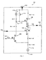
- FIG 1 is a schematic of a presently preferred voltage follower embodiment 100.
- the presently preferred embodiment 100 having a single-ended output 102 includes three transistors: a source-follower transistor T 1 104, a common-source transistor T 2 106, and a folded-cascode transistor T 3 108, and two constant current sources I 1 110 and I 2 112.
- the first and second transistors T 1 104 and T 2 106 are preferably P-channel Metal Oxide Semiconductor Field-Effect Transistors (PMOS FETs) and the third transistor T 3 108 is preferably an N-channel Metal Oxide Semiconductor Field-Effect Transistor (NMOS FET).
- PMOS FETs P-channel Metal Oxide Semiconductor Field-Effect Transistors
- NMOS FET N-channel Metal Oxide Semiconductor Field-Effect Transistor
- the output voltage of the presently preferred voltage follower embodiment 100 follows the input voltage.
- the output voltage differs from the input voltage by a gate-source voltage that depends on the threshold voltage V t of the source-follower transistor T 1 104.
- This threshold voltage V t is defined during the fabrication process where the threshold voltage V t is the minimum gate voltage necessary for the onset of current flow between the source and the drain.
- the gate-source voltage of the source-follower transistor T 1 104 depends on the bias current flowing from the source to the drain.
- the source-follower transistor T 1 104 and the folded-cascode transistor T 3 108 are biased by a current sink or the current source I 2 112.
- the drain current I DC1 of transistor T 3 108 is defined by current source I 1 110.
- the drain biasing current I DC2 of the source-follower transistor T 1 104 is preferably the difference between the currents flowing from current sources I 1 110 and I 2 112, wherein the current source I 2 112 conducts a combined direct current (DC) denoted as I DC1 + I DC2 .
- the symbol R 0 114 interconnected between the source and the gate of the common-source transistor T 2 106 illustrates the output impedance of current source I 1 110.
- R 0 104 is a significant portion of the total impedance measured from node A 116 to ground 118.
- the total impedance from node A 116 to ground 118 will depend on the transconductance of the folded-cascode transistor T 3 108, the output impedance of the current source I 2 112, and the impedance as seen into the drain of the source-follower transistor T 1 104.
- the output voltage generated at terminal V out 102 follows the input voltage received at terminal V in 120.
- the dynamic behavior of the presently preferred voltage follower embodiment 100 can be characterized by the time delays or propagation delays that occur when the input voltage changes. Since most switches exhibit nonzero switching times and inevitably have some capacitance between nodes, circuit function can depend on the delayed response of the switches, such as the transistors used in the presently preferred voltage follower embodiment 100.
- a propagation delay causes the gate source voltage V gs of the source-follower transistor T 1 104 to initially increase.
- the signal generated at V out 102 does not change instantaneously with the signal received at V in 120.
- V gs increases the conducting channel induced within the source-follower transistor T 1 104 increases and an alternating output current is correspondingly generated.
- This alternating current (AC) denoted i source follower or i sf adds to the steady state DC current I DC2 flowing through the conducting channel of the source-follower transistor T 1 104.
- I 2 112 is not configured or programmed to sink i sf , i sf is substantially added to I DC1 at the gate of the common-source transistor T 2 106 and the drain of the folded-cascode transistor T 3 108 at node A 116.
- a relatively large AC gate bias voltage supplements the DC gate bias of the common-source transistor T 2 106 due in part to the large impedance R 0 .
- These gate biases cause the conducting channel of the common-source transistor T 2 106 to decrease.
- the effective decrease in the gate source voltage bias V gs decreases the current through T 2 106 sourced by a DC supply Vdd 122, and hence, results in an AC current i commm source also denoted as i cs Eventually, the difference between the input voltage received at terminal V in 120 and the output voltage produced at terminal V out 102 comes within a voltage range defined substantially by the threshold voltage V t of the source-follower transistor T 1 104 and the DC bias current I DC2 .
- the folded-cascode transistor T 3 108, the two current-sources (I 1 110, I 2 112), and the common-source transistor T 2 106 form a current-feedback loop around the source-follower transistor T 1 104.
- the total transconductance or ratio of input AC voltage to output AC current (g m ) of this presently preferred embodiment is much higher than the transconductance of either the source-follower transistor T 1 104 or the common-source transistor T 2 106 which is set by the bias current I DC2 .
- the dynamic increase or boosting of the transconductance of the common-source transistor T 2 106 is achieved by applying an induced AC voltage to the gate of the common-source transistor T 2 106.
- the AC voltage is achieved through a high-gain current-to-voltage conversion that utilizes the sensed AC current i sf at node 116 A.
- the AC drain current i cs of the common-source transistor T 2 106 of this presently preferred embodiment 100 is boosted and has an inverted phase when compared to the AC current i sf
- the current-feedback loop minimizes the AC current i sf that flows through the source-follower transistor T 1 104 to obtain the current that flows through the source-follower that is close to the DC current I DC2 .
- the gate-source voltage of the source-follower transistor T 1 104 is a constant offset voltage between input V in 120 and output V out 102 and largely independent of the AC operation.
- the AC output current i out required to change the voltage level at the output node V out 102 is driven by the common-source transistor T 2 106 and the magnitude of i out is substantially equal to or close to the magnitude of i cs . Accordingly, the transconductance of the presently preferred voltage follower 100 is much higher than the transconductance of a source-follower transistor T 1 104 alone.
- the small-signal gain of the presently preferred voltage follower 100 is dependent on the output impedance of the voltage follower and the load impedance.
- the small-signal output impedance of the presently preferred embodiment 100 is inversely proportional to the transconductance of the common-source transistor T 2 106. Due to the boosted transconductance operation of the presently preferred embodiment 100, the signal attenuation of the circuit is small.
- the gate-source voltage of the source-follower transistor T 1 104 is almost constant even with a small-signal variation of the input signals.
- the capacitance seen by the circuit or source driving the gate of the source-follower transistor T 1 104 at terminal V in 120 is preferably determined by the gate-source capacitance and the gate-drain capacitance of the source-follower transistor T 1 104. Since the change of the gate-source voltage is preferably very small due to the operation of the current-feedback loop, the loading due to the gate-source capacitance is preferably reduced. This reduced loading effect is true even at very high frequencies due to the high bandwidth of the current-feedback loop.
- the effect of the gate-drain capacitance is preferably small too, due to the operation of the source-follower transistor T 1 104 in the saturation range and due to the low impedance at the source of the folded-cascode transistor T 3 108 which avoids a dynamic increase in Miller-effect capacitance.
- the bulk and source terminals of the source-follower transistor T 1 104 are directly connected.
- this direct continuity between the bulk and the source terminal further minimizes the signal attenuation caused by the loads that can be coupled to terminal V out 102 because the g m of the source-follower T 1 104 is optimum.
- a boost of the gate and bulk transconductance will be achieved.
- the bulk transconductance thus has a negative effect and reduces the benefits of the current-feedback transconductance boosting loop.
- the small signal attenuation in this case depends on the ratio of the gate and bulk transconductance. Preferably, this signal attenuation is less dependent or is independent of the loads coupled to the terminal V out 102.
- the above-described voltage follower embodiments 100 are not limited to the illustrated components (i.e. PMOS or NMOS transistors) as the presently preferred embodiments 100 can also comprise transistors built in a complimentary manner by exchanging PMOS FETs with NMOS FETs and NMOS FETs with PMOS FETs. Furthermore, many suitable current supplies or transistors such as cascode transistors, for example, can be used as current sources I 1 110 and I 2 112 to enhance the output impedance of the current sources just as the gate bias at terminal V bias 124 of the folded-cascode transistor T 3 108 can be driven by any suitable external or internal source or bias block or a bias voltage generator.
- the presently preferred voltage follower embodiment 100 can also be a unitary part of or integrated within a fixed or a variable presently preferred gain cell embodiment within a discrete circuit or an integrated circuit.
- the presently preferred gain cell embodiment 200 comprises two voltage followers 202 and 204 having output terminals joined by a passive component such as the illustrated resistor R 0 206.
- the latter or passive component can also be implemented with an active component such as a variable resistor or transistor.
- the transistor can be a NMOS device that operates within the linear range and is biased by a high gate voltage. By adjusting the gate voltage of the NMOS device in the linear range, the resistance value of the induced conducting channel correspondingly changes just as the variable gain of this presently preferred alternative embodiment changes.
- the presently preferred gain cell embodiment 200 utilizes a pair of transistors T 4a 208 and T 4b 210 to track and output the current that flows through R 0 206.
- the pairs of transistors T 2a 106a, T 4a 208 and T 2b 106b and T 4b 210 are in current-mirror configurations that track current flow through the common-source transistors T 2a 106a and T 2b 106b, respectively.
- transistors T 4a 208 and T 4b 210 are not matched to T 2a 106a and T 2b 106b, respectively, to provide a gain N, in other presently preferred alternative embodiments pairs of matched transistors can be used.
- the presently preferred embodiments can utilize a one to one current-mirror configuration or a one to N current-mirror configuration depending on the desired output gain generated at terminals V outp 212 and V outm 214.
- the current- mirror ratio N may also be controlled by digital logic which adjusts the gain of the presently preferred alternative embodiment by controlling transistors positioned in parallel to transistors T 4a 208 and T 4b 210.
- the current mirrors T 2a 106a, T 4a 208 and T 2b 106b, T 4b 210 provide multiple references of the current flowing through the common-source transistors T 2a 106a and T 2b 106b to a presently preferred load embodiment 216.
- the presently preferred load embodiment 216 performs a current-to-voltage conversion using a differential resistor R 1 which equals R 1a 218a plus R 1b 218b and two current sources I 3a 220 and I 3b 222 which are controlled by a common-mode feedback circuit 228.
- the common-mode voltage at output terminals V outp 212 and V outm 214 is controlled by the current sources I 3a 220-and I 3b 222 which sink the DC current flowing through the common-source transistors T 4a 106a and T 4b 106b.
- the current sources I 3a 220 and I 3b 222 sink the DC current components N x I DC2 flowing through T 4a 208 and T 4b 210 leaving only the differential currents N x i csa and N x i csb , respectively, at the output terminals V outp 212 and V outm 214.
- the voltage drop across R 1a 218a and R 1b 218b, which are both equal to 1 ⁇ 2 of R 1 , is the differential output voltage of the presently preferred embodiment and the voltage gain N x R1/R0 is set by the ratio of the resistors and the current mirror ratio. Accordingly, the presently preferred gain cell embodiment 200 can capture the difference between the signals received at terminals V inp 120a and V inm 120b by measuring the current N x i out flowing through the resistors R 1a 218a and R 1b 218b.
- a node B 224 positioned between the two resistors R 1a 218a and R 1b 218b is a virtual AC ground.
- the voltage at this node B 224 is equal to the common mode voltage at the output terminals V outp 212 and V outm 214 and can be compared to a reference voltage received at a voltage reference terminal V ref 226 by the common-mode feedback circuit 228 which adjusts the common-mode voltage of the output nodes V outp 212 and V outm, 214.
- the common-mode feedback circuit 228 compares the voltage at virtual AC ground node B 224 to an internal reference voltage or a reference voltage generated by an external source, and further controls current sources I 3a 220 and I 3b 222 to sink appropriate N x I DC2 currents.
- Figure 3 is a presently preferred alternative load embodiment 300 that can replace the load embodiment 216 of Figure 2.
- this alternative load embodiment performs a current-to-voltage conversion using the differential resistor R 1 218a and 218b and a single current source I 4 302 which is controlled by a common-mode feedback circuit 228.
- the single-current source I 4 302 conducts two times the DC current than that of one of the current sources I 3a 220 or I 3b 222 of Figure 2.
- the use of the differential resistors R 1 x 1 ⁇ 2 218a and 218b results in a DC voltage shift of the DC common-mode voltage at terminals V outp 212a and V outm 214b by (N x R 1 x1 ⁇ 2 x I DC2 ). Moreover, the capacitance of the current-source I 4 302 does not appear as a load capacitance at the output terminals V outp 212a and V outm 214b. Since the current source I 4 302 is connected to the virtual AC ground node B 224, the selection of the output impedance of current source I 4 302 can vary.
- common-mode voltage is controlled by the common-mode feedback circuit 228 by tapping the common-mode level at the virtual AC ground node B 224, by controlling the DC current. sunk by the current-source I 4 302, and taking into account the DC voltage shift through the load resistors R 1 x 1 ⁇ 2 218a and 218b.
- FIG 4 is a presently preferred third load embodiment 400 to load embodiment 216 of Figure 2 wherein the transistors T 4a 208 and T 4b 210 of Figure 2 (illustrated as current sources I 5a 402a and 1 5b 402b in Figure 4) are connected in parallel with constant current sources I 6a 406 and I 6b 408.
- this alternative load embodiment 400 avoids sinking current flowing through output terminals V outp 212 and V outm 214 directly to ground 118. Rather, the output terminals V outp 212 and V outm 214 are isolated from ground 118 by two resistors R 1 404.
- the effective resistance between V outp 212 and V outm 214 can be made about equal or equal to the effective resistance of the presently preferred load embodiment 216 of Figure 2. If R 2 is much larger than R 1 the purpose of the resistors R 2 40S is to tap the common-mode voltage of the output nodes. Moreover, the presently preferred third load embodiment 400 can process a very low common-mode level. In one presently preferred embodiment, common-mode levels below about 400 milli-volts can be attained.
- two current sources I 6a 406 and I 6b 408 are controlled by the common-mode feedback circuit 228 that also monitors the common-mode level at the virtual AC ground node B 224.
- the current sources I 6a 406 and I 6b 408 source a sufficient current to increase or decrease the common-mode level at terminals V outp 212 and V outm 214.
- Both current sources I 6a 406 and I 6b 408 can be designed to have very high output impedance because of the large DC voltage difference between VDD 122 and the common-mode voltage level at the output terminals V outp 212 and V outm 214. Hence, the small-signal gain is not attenuated as much by the parasitic output impedance of the current sources I 6a 406 and I 6b 408.
- a cascode transistor T oe 502 can be added in series to the constant current source I sa 402a and a second cascode transistor T 4c 502 can be added in series to I sb 402b shown in Figure 4. Additionally, a cascode transistor T 4c 502 can be coupled in series between T 4a 208 and the terminal V outp 212 and a second cascode transistor T 4c 502 can be coupled in series between T 4b 210 and the terminal V outm 214 of Figure 2.
- the cascode transistors one of which is shown in Figure 5, are coupled to the respective drains of T 4a 208 and T 4b 210.
- the cascode transistors are gate biased by the same DC voltage as the input common-mode voltage.
- transistors T 4c can have a W and L ratio that is N times the W and L ratio of the source-follower transistors T 1a 104a and T 1b 104b.
- the drain nodes of cascode transistors T 4c 502 will be at about the same potential as the drain nodes of the common-source transistors T 2a 106a and T 2b 106b.
- the presently preferred cascode supplements the very accurate current-mirror circuits with a very high output impedance.
- the cascode transistors may be shared between the common-mode current source transistors and the signal-path transistors T 4a 208 and T 4b 210.
- FIG. 6 illustrates presently preferred logic that can be incorporated within the embodiments of Figures 2, 3, and 4.
- transistors T 4a 208 and T 4b 210 of Figure 2 and current sources I 5a 402a and I 5b 402b of Figure 4 can each be implemented with the circuits shown in Figure 6.
- N-1 transistors T 42 - T 4N are coupled in parallel to transistor T 41 602.
- the gate bias of these transistors are controlled by digital logic 604 having N-1 control lines 606 that separately drive the selected transistor(s) by a common gate bias.
- each proceeding transistor To drive transistor T 42 - T 4N on, each proceeding transistor must be activated. For example, to turn T 43 on, T 42 and T 41 must first be on.
- a second digital control line 606 is driven to a logic high, the gate of T 43 610 will share the gate bias of T 42 608 and T 41 602. This common gate bias turns T 43 610 on.
- each transistor T 42 - T 4N shown in Figure 6 has a substantially equal width and length.
- the sequential activation of each selected transistor increases the source bias of T 4c 502 monotonically or by equal increments.
- the above-described embodiments are a unitary part of an integrated circuit, although matched transistors can also be used in alternative presently preferred discrete embodiments.
- the number of digitally actuated transistors defines the multiplication factors or current mirror ratios used in these presently preferred embodiments.
- thermometer codes are preferably used to control the switches that bias the gates.
- thermometer codes or to sequential logic.
- binary codes having "B" bit lengths and a non-sequential control can also be used.
- the gates of transistors P 1 - P* are coupled in parallel with transistor T 4a 208.
- two voltage-follower circuits 202 and 204 are used Figure 2, preferably an identical circuit would be coupled in parallel with-transistor T 4b 210.
- This configuration preferably allows combinations of output current to bias the source of P11. While a multiplier of 2 n is shown in Figure 7 (e.g., 2 n *(W/L)), many other multipliers can also be used including integer and non-integer multipliers.
- transistors P 1 - P* are directly activated by the binary codes generated by the digital logic 702 that couples transistors P 1 - P* through separate control lines.
- the activation of the digitally selected transistors can define the current mirror ratios of the presently preferred embodiments.
- the digital logic 702 drives B transistors.
- the above-described embodiments can be implemented in an integrated or discrete circuit
- the cascode transistors T 4C 502 and P 11 704 of Figures 6 and 7 can be shared between all transistors of the current mirrors.
- each of the current mirror transistors can be connected in series to an individual cascode transistor, which has a W/L ratio that is adjusted to the W/L ratio of the related current mirror transistors.
- each of the cascode transistors are connected to the output node V out .
- a high-bandwidth gain cell can comprise two high-bandwidth voltage-follower circuits 202 and 204 that copy the difference between input voltages to the differential voltage across a resistor R 0 106.
- the presently preferred voltage-followers 202 and 204 comprise source-followers 104a and 104b with enhanced transconductance that are embedded within current-feedback loops.
- the AC voltage across R 0 206 results in an AC current i out through R 0 206 that is proportional to the differential input voltage.
- the presently preferred voltage-follower circuits 202 and 204 preferably maintain the magnitude of the AC current i out that flows through R 0 206 close to the magnitude of the AC current i CS that flows through transistors T 2a 106a and T 2b , 106b.
- current-mirrors with a ratio N ⁇ 1 can be built that feed mirror currents to an output load embodiment.
- One preferred load embodiment 216 comprises two DC current-sources I 3a 220 and I 3b 222 that subtract the DC component I DC2 from the currents flowing through T 4a 208 and T 4b 210.
- the gain of the presently preferred gain-cell embodiment 200 is set by the ratio of the two resistors R 0 206 and R 1 218a and 218b and the current mirror ratio N.
- the above-descnbed embodiments can be used with many applications including repetitive storage devices, hard drives, and other electromechanical devices.
- the common-mode voltages at the input and output terminals enable the presently preferred gain cell embodiments to drive several external loads and circuits, such as circuits within a hard disk drive read-channel. Both input and output common-mode voltages can be equal thereby enabling a series connection of two gain cells without requiring additional circuitry that reduces signal bandwidth.
- the high bandwidth of the enhanced transconductance voltage-follower embodiments will not attenuate the input signals at high frequencies.
- CMOS Complementary Metal Oxide Semiconductor
Landscapes
- Engineering & Computer Science (AREA)
- Power Engineering (AREA)
- Multimedia (AREA)
- Signal Processing (AREA)
- Amplifiers (AREA)
Abstract
Description
- This invention relates to voltage followers and gain cells, and more particularly, to voltage followers used in high-bandwidth low-voltage gain cells.
- Differential circuits generate signals that are proportional to the algebraic difference between two input signals. These circuits produce an output signal only when differences exist between the input signals.
- Ideally, the output signal of a differential circuit is not dependent on the magnitude of its input signals. However, when input signals are very "weak," such signals can be so small that they cannot be processed reliably. Thus, when feeding "weak" input signals into a differential circuit, the "weak" input signals can be attenuated and the small-signal variations that can exist between these input signals cannot be detected. In other words, the information contained within the input signals and the algebraic difference between them can be lost.
- Conceptually, signal amplifiers might be used to condition input signals before the differential circuit processes the input signals. If signal amplifiers are used, the signal amplifiers must be matched and the signal amplifiers must further preserve the information contained within the input signals. One drawback to using signal amplifiers is that the resulting circuit can have a limited bandwidth. Poles of the signal amplifiers can attenuate the input signals at high frequencies, which limit the bandwidth of the differential circuit
- In the figures, like reference numerals designate similar parts throughout different views.
- Figure 1 is a schematic of a presently preferred voltage follower embodiment.
- Figure 2 is a schematic of a presently preferred gain cell embodiment incorporating Figure 1.
- Figure 3 is a schematic of a presently preferred alternative load embodiment that can be incorporated within Figure 2.
- Figure 4 is a schematic of a second presently preferred alternative load embodiment that can be incorporated within Figure 2.
- Figure 5 is a schematic of a presently preferred cascode embodiment that can be incorporated within Figures 2, 3 and 4.
- Figure 6 is a schematic of presently preferred digital logic that can be incorporated within Figures 2, 3 and 4.
- Figure 7 is a schematic of presently preferred alternative digital logic that can be incorporated within Figures 2, 3 and 4.
- The present invention is directed to a high bandwidth low-voltage gain cell that overcomes the above potential drawbacks of the prior art as it is for example disclosed in the article of T.W.Pan and A.A. Abidi, "A 30 MH2 Low-Noise CMOS Preamplifier for Disk Drive Heads", IEEE 1989, custom integrated circuits conference. The present invention is also directed to a voltage follower and buffer having an enhanced transconductance. The presently preferred embodiments minimize signal attenuation and maximize signal bandwidth in hard disk drives and other electromechanical and electronic devices. The presently preferred buffer and voltage follower includes a single-ended output, a source follower, and a current feedback loop. The current feedback loop is coupled to the single-ended output and to the source follower. The current feedback loop attains a high current gain between input and output current by using a high-gain current-to-voltage conversion with a voltage-to-current conversion performed by a common-source transistor.
- A presently preferred gain cell embodiment includes a first and a second source follower, a first and a second current feedback loop around the source follower, a first and a second current mirror circuit, a load, a common-mode feedback circuit, and a first and a second constant current source. Preferably, a differential arrangement includes the first and the second source follower circuit that is coupled to the first and the second current feedback loops, respectively. The first and the second source follower circuits are also coupled to the first and second current mirror circuits, respectively. The first and second current mirror circuits are coupled to the load which is coupled to the common-mode feedback circuit. The common-mode feedback circuit controls the constant current source which sinks mirrored currents that flow through the first and the second current mirror circuits.
- A hard drive is an electromechanical device that reads from or writes to platters made of or coated with material(s) that store data. A hard drive can include a spindle on which the platter(s) are supported, motor(s) that drive the platter(s), one or more read/write heads, head positioning mechanisms, a power supply, and a controller. In a hard disk drive a voltage buffer can be used to buffer signals driven by sources with a high source resistance to a low impedance load. A voltage follower might be used, for instance, when the voltage source resistance is much greater than the load resistance. Connecting the voltage source directly to the load without a voltage follower can result in a significant signal attenuation. In such cases, a voltage follower with a high input resistance, much greater than the load resistance, and a low output resistance can be used as a voltage buffer. Similarly, there are applications, such as within a hard drive read circuit, in which the difference between the two input signals must be detected without altering the integrity of the input signals.
- Figure 1 is a schematic of a presently preferred
voltage follower embodiment 100. The presentlypreferred embodiment 100 having a single-ended output 102 includes three transistors: a source-follower transistor T 1 104, a common-source transistor T 2 106, and a folded-cascode transistor T 3 108, and two constantcurrent sources I 1 110 and I2 112. The first andsecond transistors T 1 104 andT 2 106 are preferably P-channel Metal Oxide Semiconductor Field-Effect Transistors (PMOS FETs) and thethird transistor T 3 108 is preferably an N-channel Metal Oxide Semiconductor Field-Effect Transistor (NMOS FET). - Preferably, the output voltage of the presently preferred
voltage follower embodiment 100 follows the input voltage. In the presentlypreferred embodiment 100, the output voltage differs from the input voltage by a gate-source voltage that depends on the threshold voltage Vt of the source-follower transistor T 1 104. This threshold voltage Vt is defined during the fabrication process where the threshold voltage Vt is the minimum gate voltage necessary for the onset of current flow between the source and the drain. Furthermore, the gate-source voltage of the source-follower transistor T 1 104 depends on the bias current flowing from the source to the drain. - Preferably, the source-
follower transistor T 1 104 and the folded-cascode transistor T 3 108 are biased by a current sink or the current source I2 112. The drain current IDC1 oftransistor T 3 108 is defined by current source I1 110. The drain biasing current IDC2 of the source-follower transistor T 1 104 is preferably the difference between the currents flowing from current sources I1 110 and I2 112, wherein the current source I2 112 conducts a combined direct current (DC) denoted as IDC1 + IDC2. Thesymbol R 0 114 interconnected between the source and the gate of the common-source transistor T 2 106 illustrates the output impedance of current source I1 110. Due to a high gate resistance of the commonsource transistor T 2 106 in the presently preferred embodiment,R 0 104 is a significant portion of the total impedance measured fromnode A 116 toground 118. However, the total impedance fromnode A 116 toground 118 will depend on the transconductance of the folded-cascode transistor T 3 108, the output impedance of the current source I2 112, and the impedance as seen into the drain of the source-follower transistor T 1 104. - Preferably, the output voltage generated at
terminal V out 102 follows the input voltage received atterminal V in 120. However, the dynamic behavior of the presently preferredvoltage follower embodiment 100 can be characterized by the time delays or propagation delays that occur when the input voltage changes. Since most switches exhibit nonzero switching times and inevitably have some capacitance between nodes, circuit function can depend on the delayed response of the switches, such as the transistors used in the presently preferredvoltage follower embodiment 100. - When the input signal received at
terminal V in 120 decreases, for example, a propagation delay causes the gate source voltage Vgs of the source-follower transistor T 1 104 to initially increase. The signal generated atV out 102 does not change instantaneously with the signal received atV in 120. As Vgs increases the conducting channel induced within the source-follower transistor T 1 104 increases and an alternating output current is correspondingly generated. This alternating current (AC) denoted i source follower or isf adds to the steady state DC current IDC2 flowing through the conducting channel of the source-follower transistor T 1 104. Because I2 112 is not configured or programmed to sink isf, isf is substantially added to IDC1 at the gate of the common-source transistor T 2 106 and the drain of the folded-cascode transistor T 3 108 atnode A 116. As the AC current atnode A 116 increases, a relatively large AC gate bias voltage supplements the DC gate bias of the common-source transistor T 2 106 due in part to the large impedance R0. These gate biases cause the conducting channel of the common-source transistor T 2106 to decrease. The effective decrease in the gate source voltage bias Vgs decreases the current throughT 2 106 sourced by aDC supply Vdd 122, and hence, results in an AC current icommm source also denoted as ics Eventually, the difference between the input voltage received atterminal V in 120 and the output voltage produced atterminal V out 102 comes within a voltage range defined substantially by the threshold voltage Vt of the source-follower transistor T 1 104 and the DC bias current IDC2. - As shown, the folded-
cascode transistor T 3 108, the two current-sources (I1 110, I2 112), and the common-source transistor T 2106 form a current-feedback loop around the source-follower transistor T 1 104. The total transconductance or ratio of input AC voltage to output AC current (gm) of this presently preferred embodiment is much higher than the transconductance of either the source-follower transistor T 1 104 or the common-source transistor T 2106 which is set by the bias current IDC2. The dynamic increase or boosting of the transconductance of the common-source transistor T 2 106 is achieved by applying an induced AC voltage to the gate of the common-source transistor T 2 106. The AC voltage is achieved through a high-gain current-to-voltage conversion that utilizes the sensed AC current isf atnode 116 A. Preferably, the AC drain current ics of the common-source transistor T 2 106 of this presently preferredembodiment 100 is boosted and has an inverted phase when compared to the AC current isf The current-feedback loop minimizes the AC current isf that flows through the source-follower transistor T 1 104 to obtain the current that flows through the source-follower that is close to the DC current IDC2. Hence, the gate-source voltage of the source-follower transistor T 1 104 is a constant offset voltage betweeninput V in 120 andoutput V out 102 and largely independent of the AC operation. The AC output current iout required to change the voltage level at theoutput node V out 102 is driven by the common-source transistor T 2 106 and the magnitude of iout is substantially equal to or close to the magnitude of ics. Accordingly, the transconductance of the presently preferredvoltage follower 100 is much higher than the transconductance of a source-follower transistor T 1 104 alone. - The small-signal gain of the presently preferred
voltage follower 100 is dependent on the output impedance of the voltage follower and the load impedance. The small-signal output impedance of the presently preferredembodiment 100 is inversely proportional to the transconductance of the common-source transistor T 2 106. Due to the boosted transconductance operation of the presently preferredembodiment 100, the signal attenuation of the circuit is small. - Preferably, the gate-source voltage of the source-
follower transistor T 1 104 is almost constant even with a small-signal variation of the input signals. The capacitance seen by the circuit or source driving the gate of the source-follower transistor T 1 104 atterminal V in 120 is preferably determined by the gate-source capacitance and the gate-drain capacitance of the source-follower transistor T 1 104. Since the change of the gate-source voltage is preferably very small due to the operation of the current-feedback loop, the loading due to the gate-source capacitance is preferably reduced. This reduced loading effect is true even at very high frequencies due to the high bandwidth of the current-feedback loop. The effect of the gate-drain capacitance is preferably small too, due to the operation of the source-follower transistor T 1 104 in the saturation range and due to the low impedance at the source of the folded-cascode transistor T 3 108 which avoids a dynamic increase in Miller-effect capacitance. - As seen in Figure 1, preferably the bulk and source terminals of the source-
follower transistor T 1 104 are directly connected. Preferably, this direct continuity between the bulk and the source terminal further minimizes the signal attenuation caused by the loads that can be coupled toterminal V out 102 because the gm of the source-follower T 1 104 is optimum. In those alternative presently preferred embodiments having the bulk terminal tied to an AC ground voltage, e.g., a positive supply voltage in the case of a PMOS FET source-follower transistor T 1 104, a boost of the gate and bulk transconductance will be achieved. The bulk transconductance thus has a negative effect and reduces the benefits of the current-feedback transconductance boosting loop. The small signal attenuation in this case depends on the ratio of the gate and bulk transconductance. Preferably, this signal attenuation is less dependent or is independent of the loads coupled to theterminal V out 102. - The above-described
voltage follower embodiments 100 are not limited to the illustrated components (i.e. PMOS or NMOS transistors) as the presently preferredembodiments 100 can also comprise transistors built in a complimentary manner by exchanging PMOS FETs with NMOS FETs and NMOS FETs with PMOS FETs. Furthermore, many suitable current supplies or transistors such as cascode transistors, for example, can be used as current sources I1 110 and I2 112 to enhance the output impedance of the current sources just as the gate bias atterminal V bias 124 of the folded-cascode transistor T 3 108 can be driven by any suitable external or internal source or bias block or a bias voltage generator. - The presently preferred
voltage follower embodiment 100 can also be a unitary part of or integrated within a fixed or a variable presently preferred gain cell embodiment within a discrete circuit or an integrated circuit. As shown in Figure 2, the presently preferredgain cell embodiment 200 comprises twovoltage followers resistor R 0 206. The latter or passive component can also be implemented with an active component such as a variable resistor or transistor. In one presently preferred embodiment, the transistor can be a NMOS device that operates within the linear range and is biased by a high gate voltage. By adjusting the gate voltage of the NMOS device in the linear range, the resistance value of the induced conducting channel correspondingly changes just as the variable gain of this presently preferred alternative embodiment changes. - The presently preferred
gain cell embodiment 200 utilizes a pair oftransistors T 4a 208 andT 4b 210 to track and output the current that flows throughR 0 206. Preferably, the pairs of transistors T2a 106a,T 4a 208 andT 2b 106b andT 4b 210 are in current-mirror configurations that track current flow through the common-source transistors T2a 106a andT 2b 106b, respectively. Althoughtransistors T 4a 208 andT 4b 210 are not matched to T2a 106a andT 2b 106b, respectively, to provide a gain N, in other presently preferred alternative embodiments pairs of matched transistors can be used. Accordingly, the presently preferred embodiments can utilize a one to one current-mirror configuration or a one to N current-mirror configuration depending on the desired output gain generated atterminals V outp 212 andV outm 214. The current- mirror ratio N may also be controlled by digital logic which adjusts the gain of the presently preferred alternative embodiment by controlling transistors positioned in parallel totransistors T 4a 208 andT 4b 210. - As shown, the current mirrors T2a 106a,
T 4a 208 andT 2b 106b,T 4b 210 provide multiple references of the current flowing through the common-source transistors T2a 106a andT 2b 106b to a presently preferredload embodiment 216. Preferably, the presently preferredload embodiment 216 performs a current-to-voltage conversion using a differential resistor R1 which equalsR 1a 218a plusR 1b 218b and two current sources I3a 220 and I3b 222 which are controlled by a common-mode feedback circuit 228. Preferably, the common-mode voltage atoutput terminals V outp 212 andV outm 214 is controlled by the current sources I3a 220-and I3b 222 which sink the DC current flowing through the common-source transistors T4a 106a andT 4b 106b. Preferably, the current sources I3a 220 and I3b 222 sink the DC current components N x IDC2 flowing throughT 4a 208 andT 4b 210 leaving only the differential currents N x icsa and N x icsb, respectively, at theoutput terminals V outp 212 andV outm 214. - The voltage drop across
R 1a 218a andR 1b 218b, which are both equal to ½ of R1, is the differential output voltage of the presently preferred embodiment and the voltage gain N x R1/R0 is set by the ratio of the resistors and the current mirror ratio. Accordingly, the presently preferredgain cell embodiment 200 can capture the difference between the signals received atterminals V inp 120a andV inm120b by measuring the current N x iout flowing through theresistors R 1a 218a andR 1b 218b. - Preferably, a
node B 224 positioned between the tworesistors R 1a 218a andR 1b 218b is a virtual AC ground. The voltage at thisnode B 224 is equal to the common mode voltage at theoutput terminals V outp 212 andV outm 214 and can be compared to a reference voltage received at a voltagereference terminal V ref 226 by the common-mode feedback circuit 228 which adjusts the common-mode voltage of theoutput nodes V outp 212 andV outm, 214. Preferably, the common-mode feedback circuit 228 compares the voltage at virtual ACground node B 224 to an internal reference voltage or a reference voltage generated by an external source, and further controls current sources I3a 220 and I3b 222 to sink appropriate N x IDC2 currents. - Figure 3 is a presently preferred
alternative load embodiment 300 that can replace theload embodiment 216 of Figure 2. Preferably, this alternative load embodiment performs a current-to-voltage conversion using thedifferential resistor R mode feedback circuit 228. Preferably, the single-current source I4 302 conducts two times the DC current than that of one of the current sources I3a 220 or I3b 222 of Figure 2. The use of the differential resistors R1 x ½ 218a and 218b results in a DC voltage shift of the DC common-mode voltage atterminals V outp 212a andV outm 214b by (N x R1x½ x IDC2). Moreover, the capacitance of the current-source I4 302 does not appear as a load capacitance at theoutput terminals V outp 212a andV outm 214b. Since the current source I4 302 is connected to the virtual ACground node B 224, the selection of the output impedance of current source I4 302 can vary. Finally, it should be noted that common-mode voltage is controlled by the common-mode feedback circuit 228 by tapping the common-mode level at the virtual ACground node B 224, by controlling the DC current. sunk by the current-source I4 302, and taking into account the DC voltage shift through the load resistors R1 x ½ 218a and 218b. - Figure 4 is a presently preferred
third load embodiment 400 to loadembodiment 216 of Figure 2 wherein thetransistors T 4a 208 andT 4b 210 of Figure 2 (illustrated as current sources I5a 402a and 15b 402b in Figure 4) are connected in parallel with constant current sources I6a 406 and I6b 408. As shown, thisalternative load embodiment 400 avoids sinking current flowing throughoutput terminals V outp 212 andV outm 214 directly toground 118. Rather, theoutput terminals V outp 212 andV outm 214 are isolated fromground 118 by tworesistors R 1 404. Because these resistors R1 404 are in parallel with two other resistors R2 405 that couple terminals Voutp 212 toV omm 214, the effective resistance betweenV outp 212 andV outm 214 can be made about equal or equal to the effective resistance of the presently preferredload embodiment 216 of Figure 2. If R2 is much larger than R1 the purpose of the resistors R2 40S is to tap the common-mode voltage of the output nodes. Moreover, the presently preferredthird load embodiment 400 can process a very low common-mode level. In one presently preferred embodiment, common-mode levels below about 400 milli-volts can be attained. - As further shown in Figure 4, two current sources I6a 406 and I6b 408 are controlled by the common-
mode feedback circuit 228 that also monitors the common-mode level at the virtual ACground node B 224. Preferably, the current sources I6a 406 and I6b 408 source a sufficient current to increase or decrease the common-mode level atterminals V outp 212 andV outm 214. Both current sources I6a 406 and I6b 408 can be designed to have very high output impedance because of the large DC voltage difference betweenVDD 122 and the common-mode voltage level at theoutput terminals V outp 212 andV outm 214. Hence, the small-signal gain is not attenuated as much by the parasitic output impedance of the current sources I6a 406 and I6b 408. - To improve the output impedance of the common-mode feedback current-sources,, a
cascode transistor T oe 502 can be added in series to the constant current source Isa 402a and a secondcascode transistor T 4c 502 can be added in series to Isb 402b shown in Figure 4. Additionally, acascode transistor T 4c 502 can be coupled in series betweenT 4a 208 and theterminal V outp 212 and a secondcascode transistor T 4c 502 can be coupled in series betweenT 4b 210 and theterminal V outm 214 of Figure 2. Preferably, the cascode transistors, one of which is shown in Figure 5, are coupled to the respective drains ofT 4a 208 andT 4b 210. Preferably, the cascode transistors are gate biased by the same DC voltage as the input common-mode voltage. When fabricated within an integrated circuit, transistors T4c can have a W and L ratio that is N times the W and L ratio of the source-follower transistors T 1a 104a andT 1b 104b. Accordingly, in this presently preferred embodiment, the drain nodes ofcascode transistors T 4c 502 will be at about the same potential as the drain nodes of the common-source transistors T2a 106a andT 2b 106b. Accordingly, the presently preferred cascode supplements the very accurate current-mirror circuits with a very high output impedance. The cascode transistors may be shared between the common-mode current source transistors and the signal-path transistors T 4a 208 andT 4b 210. - Figure 6 illustrates presently preferred logic that can be incorporated within the embodiments of Figures 2, 3, and 4. In these presently preferred embodiments,
transistors T 4a 208 andT 4b 210 of Figure 2 and current sources I5a 402a and I5b 402b of Figure 4 can each be implemented with the circuits shown in Figure 6. In these presently preferred embodiments, N-1 transistors T42 - T4N are coupled in parallel totransistor T 41 602. The gate bias of these transistors are controlled bydigital logic 604 having N-1control lines 606 that separately drive the selected transistor(s) by a common gate bias. To drive transistor T42 - T4N on, each proceeding transistor must be activated. For example, to turn T43 on, T42 and T41 must first be on. When a seconddigital control line 606 is driven to a logic high, the gate ofT 43 610 will share the gate bias ofT 42 608 andT 41 602. This common gate bias turnsT 43 610 on. - Preferably, each transistor T42 - T4N shown in Figure 6 has a substantially equal width and length. The sequential activation of each selected transistor increases the source bias of
T 4c 502 monotonically or by equal increments. Preferably, the above-described embodiments are a unitary part of an integrated circuit, although matched transistors can also be used in alternative presently preferred discrete embodiments. Preferably, the number of digitally actuated transistors defines the multiplication factors or current mirror ratios used in these presently preferred embodiments. Moreover, thermometer codes are preferably used to control the switches that bias the gates. - The above-described embodiments are not limited to thermometer codes or to sequential logic. As shown in Figure 7, binary codes having "B" bit lengths and a non-sequential control can also be used. Preferably, the gates of transistors P1 - P* are coupled in parallel with
transistor T 4a 208. Since two voltage-follower circuits transistor T 4b 210. This configuration preferably allows combinations of output current to bias the source of P11. While a multiplier of 2n is shown in Figure 7 (e.g., 2n*(W/L)), many other multipliers can also be used including integer and non-integer multipliers. Preferably, transistors P1 - P* are directly activated by the binary codes generated by thedigital logic 702 that couples transistors P1 - P* through separate control lines. The activation of the digitally selected transistors can define the current mirror ratios of the presently preferred embodiments. A shown, thedigital logic 702 drives B transistors. Moreover, the above-described embodiments can be implemented in an integrated or discrete circuit - Preferably, the
cascode transistors T 4C 502 andP 11 704 of Figures 6 and 7 can be shared between all transistors of the current mirrors. To improve the accuracy of the current mirrors, each of the current mirror transistors can be connected in series to an individual cascode transistor, which has a W/L ratio that is adjusted to the W/L ratio of the related current mirror transistors. In these presently preferred embodiments, each of the cascode transistors are connected to the output node Vout. - From the foregoing detailed description, it should be apparent that a high-bandwidth gain cell can comprise two high-bandwidth voltage-
follower circuits resistor R 0 106. The presently preferred voltage-followers followers R 0 206, results in an AC current iout throughR 0 206 that is proportional to the differential input voltage. The presently preferred voltage-follower circuits R 0 206 close to the magnitude of the AC current iCS that flows through transistors T2a 106a and T2b, 106b. By using twoadditional devices T 4a 208 andT 4b 210 current-mirrors with a ratio N≥1 can be built that feed mirror currents to an output load embodiment. Onepreferred load embodiment 216 comprises two DC current-sources I3a 220 and I3b 222 that subtract the DC component IDC2 from the currents flowing throughT 4a 208 andT 4b 210. Provided that the impedance of the external loads connected toterminals V outp 212 andV outm 214 are high and the output impedance of the current-sources I2a 112a andI 2b 112b are high, the AC current iout will flow throughresistor R cell embodiment 200 is set by the ratio of the tworesistors R 0 206 andR - The above-descnbed embodiments can be used with many applications including repetitive storage devices, hard drives, and other electromechanical devices. The common-mode voltages at the input and output terminals enable the presently preferred gain cell embodiments to drive several external loads and circuits, such as circuits within a hard disk drive read-channel. Both input and output common-mode voltages can be equal thereby enabling a series connection of two gain cells without requiring additional circuitry that reduces signal bandwidth. The high bandwidth of the enhanced transconductance voltage-follower embodiments will not attenuate the input signals at high frequencies. Moreover, there is a low attenuation of the differential input voltages when the presently preferred voltage follower embodiments are used to buffer
R 0 206. Moreover, the above-described presently preferred embodiments can operate at very low supply voltages, such as, for example, at less than or equal to about two volts (i.e., Vdd ⇐ 2V DC). Furthermore, the presently preferred embodiments can be implemented entirely in Complementary Metal Oxide Semiconductor (CMOS) technology.
Claims (21)
- A hard disk drive read-channel gain cell, comprising:a first and a second current feedback loop;a differential pair comprising a first source follower circuit (104a) and a second source follower circuit (104b), the first source follower circuit being coupled to the first current feedback loop and the second source follower circuit being coupled to the second current feedback loop;a first current mirror circuit (208, 106a) coupled to the first source follower circuit;a second current mirror (210, 106b) circuit coupled to the second source follower circuit;a load (216) coupled to the first and the second current mirror circuit;a common-mode feedback circuit (228) coupled to the load; anda constant current source (220, 222) coupled to the first and the second current mirror circuits and to the common-mode feedback circuit, the constant current source being configured to sink mirrored currents that flow through the first and the second current mirror circuits when controlled by the common-mode feedback circuit.
- The hard disk drive read-channel gain cell of claim 1, wherein the first and the second feedback loops each comprise a first and a second constant current source (112a, 112b) and a folded cascode circuit, wherein each of the first and the second constant current sources bias the folded cascode circuit.
- The hard disk drive read-channel gain cell of claim 2, wherein each of the first and the second current mirror circuits comprise a common source circuit (106a, 106b) coupled to the second constant current source and the folded cascode circuit.
- The hard disk drive read-channel gain cell of claim 1, further comprising a third constant current source (116a, 116b), wherein each of the first and second current mirror circuits are biased by the respective third constant current source.
- The hard disk drive read-channel gain cell of claim 1, further comprising a second load (206), the second load being coupled between the differential pair.
- The hard disk drive read-channel gain cell of claim 5, wherein the first and the second loads comprise resistive loads.
- The hard disk drive read-channel gain cell of claim 6, wherein at least one of the first and the second loads is a MOS transistor or a combination of MOS transistors operating in a linear range.
- The hard disk drive read-channel gain cell of claim 6, wherein at least one of the first and the second loads comprises a differential load.
- The hard disk drive read-channel gain cell of claim 1, wherein the constant current source comprises a first and a second constant current source, wherein the first constant current source is coupled to the first current mirror circuit and the second constant current source is coupled to the second current mirror circuit.
- The hard disk drive read-channel gain cell of claim 1, wherein the current-mirror ratio N may be larger than unity and may be controlled by a digital logic.
- The hard disk drive read-channel gain cell of claim 9, wherein the load comprises a differential resistive load interconnected at a common node, the common node being coupled to the common-mode feedback circuit.
- The hard disk drive read-channel gain cell of claim 9, wherein the constant current source comprises a first and a second constant current source, wherein the first constant current source is coupled in parallel to the first current mirror circuit and the second constant current source is coupled in parallel to the second current mirror circuit.
- The hard disk drive read-channel gain cell of claim 9, wherein the first and the second current mirror circuits each comprise a third constant current source coupled to a voltage supply.
- The hard disk drive read-channel gain cell of claim 12, wherein the first and the second current mirror are coupled to ground by a first and a second resistor, respectively.
- The hard disk drive read-channel gain cell of claim 14 further comprising a first and a second output, the first output coupling the second output through a differential resistor and being coupled to ground by the first and the second resistors, respectively.
- The hard disk drive read-channel gain cell of claim 15 wherein the common-mode feedback circuit is coupled to a common node that interconnects the differential resistor.
- The hard disk drive read-channel gain cell of claim 2, wherein each of the first and the second current mirror circuits comprises cascode circuits, respectively.
- The hard disk drive read-channel gain cell of claim 1 wherein the differential pair, the first current mirror circuit, the second current mirror circuit, the common-mode feedback circuit, and the constant current source are configured to operate at a supply voltage below about two volts.
- The hard disk drive read-channel gain cell of claim 1, wherein the differential pair, the first current mirror circuit, the second current mirror circuit, the common-mode feedback circuit, and the constant current source are CMOS devices.
- The hard disk drive read-channel gain cell of claim 1, further comprising a pair of output terminals and a second hard disk drive read-channel gain cell, wherein the output terminals are coupled to the first and the second current mirror circuits and are directly connected to the second hard disk drive read-channel gain cell.
- A hard disk drive read-channel gain cell, comprising:a pair of output terminals (212, 214);a first and a second current feedback loop; wherein the first and the second feedback loops each comprise a first and a second constant current source and a folded cascode circuit, and wherein each of the first and the second constant current sources bias the folded cascode circuit;a differential pair comprising a first source follower circuit (104a) and a second source follower circuit (104b), the first source follower circuit being coupled to the first current feedback loop and the second source follower circuit being coupled to the second current feedback loop;a first current mirror circuit coupled to the first source follower circuit; the first current mirror circuit comprising a cascode circuit coupled to one of the output terminals;a second current mirror coupled to the second source follower circuit; the second current mirror circuit comprising a cascode circuit coupled to one of the output terminals;a differential load (216) coupled between the first and the second current mirror circuits;a common-mode feedback circuit coupled to the load (228); anda third constant current source (220, 222) coupled to the first and the second current mirror circuits and to the common-mode feedback circuit, the third constant current source being configured to sink mirrored currents that flow through the first and the second current mirror circuits when controlled by the common-mode feedback circuit.
Applications Claiming Priority (3)
| Application Number | Priority Date | Filing Date | Title |
|---|---|---|---|
| US865744 | 2001-05-25 | ||
| US09/865,744 US6580326B2 (en) | 2001-05-25 | 2001-05-25 | High-bandwidth low-voltage gain cell and voltage follower having an enhanced transconductance |
| PCT/US2002/016758 WO2002097975A2 (en) | 2001-05-25 | 2002-05-24 | High-bandwidth low-voltage gain cell and voltage follower having an enhanced transconductance |
Publications (2)
| Publication Number | Publication Date |
|---|---|
| EP1417752A2 EP1417752A2 (en) | 2004-05-12 |
| EP1417752B1 true EP1417752B1 (en) | 2006-07-12 |
Family
ID=25346127
Family Applications (1)
| Application Number | Title | Priority Date | Filing Date |
|---|---|---|---|
| EP02726934A Expired - Lifetime EP1417752B1 (en) | 2001-05-25 | 2002-05-24 | High-bandwidth low-voltage gain cell and voltage follower having an enhanced transconductance |
Country Status (5)
| Country | Link |
|---|---|
| US (1) | US6580326B2 (en) |
| EP (1) | EP1417752B1 (en) |
| CN (1) | CN1260880C (en) |
| DE (1) | DE60213101T2 (en) |
| WO (1) | WO2002097975A2 (en) |
Families Citing this family (31)
| Publication number | Priority date | Publication date | Assignee | Title |
|---|---|---|---|---|
| US6847251B2 (en) * | 2001-01-11 | 2005-01-25 | Media Tek, Inc. | Differential charge pump circuit |
| US6552865B2 (en) * | 2001-05-25 | 2003-04-22 | Infineon Technologies Ag | Diagnostic system for a read/write channel in a disk drive |
| JP2003124757A (en) * | 2001-10-16 | 2003-04-25 | Texas Instr Japan Ltd | Method and apparatus for reducing the effects of early effects |
| DE60217881D1 (en) * | 2002-11-28 | 2007-03-15 | St Microelectronics Srl | Circuit device for producing a non-linear scaling network with reactive elements |
| US6924674B2 (en) * | 2003-10-27 | 2005-08-02 | Agere Systems Inc. | Composite source follower |
| US7151410B2 (en) * | 2003-12-17 | 2006-12-19 | Agere Systems Inc. | Class AB enhanced transconductance source follower |
| US7236030B2 (en) * | 2004-06-30 | 2007-06-26 | Texas Instruments Incorporated | Method to implement hysteresis in a MOSFET differential pair input stage |
| US7498858B2 (en) * | 2004-11-01 | 2009-03-03 | Hewlett-Packard Development Company, L.P. | Interpolator systems with linearity adjustments and related methods |
| US8179194B2 (en) * | 2009-05-05 | 2012-05-15 | Futurewei Technologies, Inc. | System and method for a reference generator |
| CN101881984B (en) * | 2009-05-05 | 2013-04-24 | 华为技术有限公司 | Reference signal generator and method and system thereof |
| FR2955219B1 (en) * | 2010-01-14 | 2012-08-31 | St Microelectronics Sa | AMPLIFIER DEPHASEUR |
| CN102324896B (en) * | 2011-07-11 | 2014-07-09 | 复旦大学 | Low-noise broadband amplifier with linearity compensation |
| CN103019287B (en) * | 2011-09-27 | 2015-12-16 | 联发科技(新加坡)私人有限公司 | Control circuit and circuit control method |
| DE102011122894B4 (en) | 2011-09-30 | 2019-05-09 | Intel Deutschland Gmbh | Circuit and power amplifier |
| CN104518740A (en) * | 2013-09-29 | 2015-04-15 | Lsi公司 | Amplifier of voltage follower |
| US9525391B2 (en) * | 2014-03-05 | 2016-12-20 | Mediatek Singapore Pte. Ltd. | Fully differential class A/AB amplifier and method thereof |
| EP2945286B1 (en) * | 2014-05-12 | 2018-06-27 | ams AG | Amplifier arrangement and amplification method |
| US10063199B2 (en) * | 2016-06-09 | 2018-08-28 | Analog Devices Global | Buffer with increased headroom |
| US10734958B2 (en) * | 2016-08-09 | 2020-08-04 | Mediatek Inc. | Low-voltage high-speed receiver |
| CN106537276B (en) * | 2016-08-16 | 2018-02-13 | 深圳市汇顶科技股份有限公司 | a linear regulator |
| CN107196644A (en) * | 2017-05-07 | 2017-09-22 | 长沙方星腾电子科技有限公司 | A kind of analogue buffer |
| US10250999B1 (en) | 2017-09-18 | 2019-04-02 | Infineon Technologies Ag | PVT compensated resistive biasing architecture for a capacitive sensor |
| FR3085564A1 (en) | 2018-09-05 | 2020-03-06 | Stmicroelectronics Sa | VARIABLE GAIN AMPLIFIER INCORPORATED IN A RECEPTION CHAIN |
| DE102018129910A1 (en) * | 2018-11-27 | 2020-05-28 | Intel Corporation | Concept for a buffered inverted voltage follower and for a voltage regulator with a low dropout |
| US10614860B1 (en) * | 2019-04-15 | 2020-04-07 | Micron Technology, Inc. | Systems for discharging leakage current over a range of process, voltage, temperature (PVT) conditions |
| CN110212876A (en) * | 2019-06-24 | 2019-09-06 | 南京芯耐特半导体有限公司 | Follower circuit structure with built-in negative-feedback |
| CN111313852B (en) * | 2020-05-15 | 2020-09-11 | 微龛(广州)半导体有限公司 | Drive amplifier and analog-to-digital converter |
| CN113972558B (en) * | 2021-10-18 | 2023-09-29 | 厦门优迅高速芯片有限公司 | Optical device drive circuits, optical components and electronic equipment |
| US12332679B2 (en) | 2022-08-16 | 2025-06-17 | Apple Inc. | High output impedance current mirror circuit |
| US20250391438A1 (en) * | 2024-06-21 | 2025-12-25 | Marvell Asia Pte Ltd | Differential Current-Mode Driver for Microwave Assisted Magnetic Recording |
| CN120956227B (en) * | 2025-10-14 | 2026-03-10 | 浙江地芯引力科技有限公司 | Resistance voltage coefficient compensation circuit in adjustable gain amplifier and electronic equipment |
Family Cites Families (14)
| Publication number | Priority date | Publication date | Assignee | Title |
|---|---|---|---|---|
| NL7102199A (en) * | 1971-02-19 | 1972-08-22 | ||
| FR2488077A1 (en) * | 1980-07-31 | 1982-02-05 | Thomson Csf | LOW IMPEDANCE OUTPUT STAGE FOR CAPACITIVE OR DIRECT COUPLING |
| US4420726A (en) * | 1981-06-04 | 1983-12-13 | Rca Corporation | Voltage-followers with low offset voltages |
| US4835489A (en) * | 1987-02-13 | 1989-05-30 | National Semiconductor Corporation | Single-ended, feed-forward gain stage |
| US4825174A (en) * | 1988-06-20 | 1989-04-25 | American Telephone And Telegraph Company, At&T Bell Laboratories | Symmetric integrated amplifier with controlled DC offset voltage |
| JP2517472B2 (en) * | 1990-10-26 | 1996-07-24 | 菊水電子工業株式会社 | FET buffer amplifier |
| US5198782A (en) * | 1991-01-15 | 1993-03-30 | Crystal Semiconductor | Low distortion amplifier output stage for dac |
| US5221909A (en) * | 1992-04-30 | 1993-06-22 | Raytheon Company | Active load biasing circuit |
| JP2944398B2 (en) * | 1993-07-05 | 1999-09-06 | 日本電気株式会社 | MOS differential voltage-current converter |
| US5712739A (en) * | 1993-11-08 | 1998-01-27 | Kabushiki Kaisha Toshiba | Magnetic disk drive system with a composite head unit including a magnetoresistive read only head and an inductive write only head |
| US5469104A (en) * | 1994-03-28 | 1995-11-21 | Elantec, Inc. | Active folded cascode |
| US5717536A (en) * | 1995-09-19 | 1998-02-10 | Vtc Inc. | Single-ended cascode amplifier for magnetoresistive sensors |
| DE69629549T2 (en) * | 1995-11-21 | 2004-06-17 | Koninklijke Philips Electronics N.V. | ARRANGEMENT WITH A MAGNETIC WRITING HEAD AND WRITING AMPLIFIER WITH CAPACITIVE, FORWARD-COUPLED COMPENSATION |
| JPH11195202A (en) * | 1997-11-04 | 1999-07-21 | Hitachi Ltd | Small signal amplifier and magnetic disk memory device using the same |
-
2001
- 2001-05-25 US US09/865,744 patent/US6580326B2/en not_active Expired - Lifetime
-
2002
- 2002-05-24 CN CNB028106679A patent/CN1260880C/en not_active Expired - Lifetime
- 2002-05-24 WO PCT/US2002/016758 patent/WO2002097975A2/en not_active Ceased
- 2002-05-24 EP EP02726934A patent/EP1417752B1/en not_active Expired - Lifetime
- 2002-05-24 DE DE60213101T patent/DE60213101T2/en not_active Expired - Lifetime
Also Published As
| Publication number | Publication date |
|---|---|
| DE60213101D1 (en) | 2006-08-24 |
| CN1260880C (en) | 2006-06-21 |
| DE60213101T2 (en) | 2007-01-11 |
| WO2002097975A2 (en) | 2002-12-05 |
| US6580326B2 (en) | 2003-06-17 |
| CN1524340A (en) | 2004-08-25 |
| WO2002097975A3 (en) | 2004-03-11 |
| US20020175761A1 (en) | 2002-11-28 |
| EP1417752A2 (en) | 2004-05-12 |
Similar Documents
| Publication | Publication Date | Title |
|---|---|---|
| US6580326B2 (en) | High-bandwidth low-voltage gain cell and voltage follower having an enhanced transconductance | |
| US6356153B1 (en) | Rail-to-rail input/output operational amplifier and method | |
| JP3152922B2 (en) | Current mirror circuit | |
| US5220207A (en) | Load current monitor for MOS driver | |
| US7088180B2 (en) | Programmable gain current amplifier | |
| US7898330B2 (en) | Class AB amplifier systems | |
| US4379267A (en) | Low power differential amplifier | |
| US5177450A (en) | Cmos power amplifier | |
| US6433637B1 (en) | Single cell rail-to-rail input/output operational amplifier | |
| KR100324452B1 (en) | Feedback Amplifier for Increased Adjusted Cascode Gain | |
| US6891433B2 (en) | Low voltage high gain amplifier circuits | |
| US6133764A (en) | Comparator circuit and method | |
| US6924702B2 (en) | Low supply voltage and self-biased high speed receiver | |
| US6741130B2 (en) | High-speed output transconductance amplifier capable of operating at different voltage levels | |
| US6784698B1 (en) | Sense amplifier with improved common mode rejection | |
| US6326846B1 (en) | Low voltage fet differential amplifier and method | |
| CA1158727A (en) | Driver circuit having reduced cross-over distortion | |
| US7167052B2 (en) | Low voltage differential amplifier circuit for wide voltage range operation | |
| US6124760A (en) | Transconductance control circuit for rail-to-rail (RTR) differential input terminal | |
| EP1254511B1 (en) | Differential amplifier with gain substantially independent of temperature | |
| US5515006A (en) | Low distortion efficient large swing CMOS amplifier output | |
| US6930530B1 (en) | High-speed receiver for high I/O voltage and low core voltage | |
| US20020109548A1 (en) | Power amplifying circuit | |
| US20050253645A1 (en) | Current output stages | |
| US5710516A (en) | Input logic signal buffer circuits |
Legal Events
| Date | Code | Title | Description |
|---|---|---|---|
| PUAI | Public reference made under article 153(3) epc to a published international application that has entered the european phase |
Free format text: ORIGINAL CODE: 0009012 |
|
| 17P | Request for examination filed |
Effective date: 20031211 |
|
| AK | Designated contracting states |
Kind code of ref document: A2 Designated state(s): AT BE CH CY DE DK ES FI FR GB GR IE IT LI LU MC NL PT SE TR |
|
| RIN1 | Information on inventor provided before grant (corrected) |
Inventor name: BLON, THOMAS Inventor name: CYRUSIAN, SASA Inventor name: BACH, ELMAR Inventor name: FRANCK, STEPHEN |
|
| GRAP | Despatch of communication of intention to grant a patent |
Free format text: ORIGINAL CODE: EPIDOSNIGR1 |
|
| RBV | Designated contracting states (corrected) |
Designated state(s): DE FR GB IE IT NL |
|
| GRAS | Grant fee paid |
Free format text: ORIGINAL CODE: EPIDOSNIGR3 |
|
| GRAA | (expected) grant |
Free format text: ORIGINAL CODE: 0009210 |
|
| AK | Designated contracting states |
Kind code of ref document: B1 Designated state(s): DE FR GB IE IT NL |
|
| PG25 | Lapsed in a contracting state [announced via postgrant information from national office to epo] |
Ref country code: IT Free format text: LAPSE BECAUSE OF FAILURE TO SUBMIT A TRANSLATION OF THE DESCRIPTION OR TO PAY THE FEE WITHIN THE PRESCRIBED TIME-LIMIT;WARNING: LAPSES OF ITALIAN PATENTS WITH EFFECTIVE DATE BEFORE 2007 MAY HAVE OCCURRED AT ANY TIME BEFORE 2007. THE CORRECT EFFECTIVE DATE MAY BE DIFFERENT FROM THE ONE RECORDED. Effective date: 20060712 Ref country code: NL Free format text: LAPSE BECAUSE OF FAILURE TO SUBMIT A TRANSLATION OF THE DESCRIPTION OR TO PAY THE FEE WITHIN THE PRESCRIBED TIME-LIMIT Effective date: 20060712 |
|
| REG | Reference to a national code |
Ref country code: GB Ref legal event code: FG4D |
|
| REG | Reference to a national code |
Ref country code: IE Ref legal event code: FG4D |
|
| REF | Corresponds to: |
Ref document number: 60213101 Country of ref document: DE Date of ref document: 20060824 Kind code of ref document: P |
|
| NLV1 | Nl: lapsed or annulled due to failure to fulfill the requirements of art. 29p and 29m of the patents act | ||
| EN | Fr: translation not filed | ||
| PLBE | No opposition filed within time limit |
Free format text: ORIGINAL CODE: 0009261 |
|
| STAA | Information on the status of an ep patent application or granted ep patent |
Free format text: STATUS: NO OPPOSITION FILED WITHIN TIME LIMIT |
|
| 26N | No opposition filed |
Effective date: 20070413 |
|
| PG25 | Lapsed in a contracting state [announced via postgrant information from national office to epo] |
Ref country code: FR Free format text: LAPSE BECAUSE OF FAILURE TO SUBMIT A TRANSLATION OF THE DESCRIPTION OR TO PAY THE FEE WITHIN THE PRESCRIBED TIME-LIMIT Effective date: 20070511 |
|
| PG25 | Lapsed in a contracting state [announced via postgrant information from national office to epo] |
Ref country code: IE Free format text: LAPSE BECAUSE OF NON-PAYMENT OF DUE FEES Effective date: 20070524 |
|
| PG25 | Lapsed in a contracting state [announced via postgrant information from national office to epo] |
Ref country code: FR Free format text: LAPSE BECAUSE OF FAILURE TO SUBMIT A TRANSLATION OF THE DESCRIPTION OR TO PAY THE FEE WITHIN THE PRESCRIBED TIME-LIMIT Effective date: 20060712 |
|
| PGFP | Annual fee paid to national office [announced via postgrant information from national office to epo] |
Ref country code: GB Payment date: 20170519 Year of fee payment: 16 |
|
| PGFP | Annual fee paid to national office [announced via postgrant information from national office to epo] |
Ref country code: DE Payment date: 20170718 Year of fee payment: 16 |
|
| REG | Reference to a national code |
Ref country code: DE Ref legal event code: R119 Ref document number: 60213101 Country of ref document: DE |
|
| GBPC | Gb: european patent ceased through non-payment of renewal fee |
Effective date: 20180524 |
|
| PG25 | Lapsed in a contracting state [announced via postgrant information from national office to epo] |
Ref country code: GB Free format text: LAPSE BECAUSE OF NON-PAYMENT OF DUE FEES Effective date: 20180524 Ref country code: DE Free format text: LAPSE BECAUSE OF NON-PAYMENT OF DUE FEES Effective date: 20181201 |