EP1416720A1 - A process and system for processing signals arranged in a Bayer pattern - Google Patents
A process and system for processing signals arranged in a Bayer pattern Download PDFInfo
- Publication number
- EP1416720A1 EP1416720A1 EP02425655A EP02425655A EP1416720A1 EP 1416720 A1 EP1416720 A1 EP 1416720A1 EP 02425655 A EP02425655 A EP 02425655A EP 02425655 A EP02425655 A EP 02425655A EP 1416720 A1 EP1416720 A1 EP 1416720A1
- Authority
- EP
- European Patent Office
- Prior art keywords
- pixels
- format
- video signals
- row
- digital video
- Prior art date
- Legal status (The legal status is an assumption and is not a legal conclusion. Google has not performed a legal analysis and makes no representation as to the accuracy of the status listed.)
- Granted
Links
Images

Classifications
-
- H—ELECTRICITY
- H04—ELECTRIC COMMUNICATION TECHNIQUE
- H04N—PICTORIAL COMMUNICATION, e.g. TELEVISION
- H04N1/00—Scanning, transmission or reproduction of documents or the like, e.g. facsimile transmission; Details thereof
- H04N1/46—Colour picture communication systems
- H04N1/64—Systems for the transmission or the storage of the colour picture signal; Details therefor, e.g. coding or decoding means therefor
- H04N1/648—Transmitting or storing the primary (additive or subtractive) colour signals; Compression thereof
Definitions
- the invention refers to a technique used for the reduction of bus transitions, or rather for the reduction of what is currently known as switching activity (SA).
- SA switching activity
- the invention has been developed with particular attention to the possible application in the transmission of signals in the Bayer format.
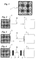
- Digital signals in the Bayer format such as those provided by an image sensor, equipping a camera for example, have the format shown in Figure 1.
- a matrix format is being dealt with in which each row is alternatively coded with two colours: odd rows are alternatively coded with the red and green colours, while even rows are alternatively coded with the green and blue colours.
- bus inverter BI
- the problem can be faced, at least in principle, by applying data encoding techniques on the bus B aimed at reducing switching activity.
- bus inverter BI
- the results deriving from the application of this technique can vary, and in quite a significant manner, depending on the type of data being transmitted.
- the present invention sets itself the object of providing a solution capable of constituting the solution of choice for an application context of the type represented in Figure 2.
- the invention is based on the idea of performing an ordered encoding of the sequence of Bayer format data in input to the transmission bus. The purpose of this is to reduce the transitions during transmission on the bus, consequently realizing the subsequent reordering of the data into the Bayer format at the output of the transmission bus.
- This communication absorbs a large quantity of power due to the effect of induced transitions on the connection bus B.
- the senor has n pixels per row (five pixels in the case of the example illustrated herein), or rather n columns and that there are a total of m rows (in this case totalling five in number).
- Each colour is first transmitted with k/2 bits of the upper part (from bit k-1 to bit k/2) and then the k/2 bits of the lower part (from bit [k/2-1] to bit 0) .
- the idea at the base of the invention is therefore that of reorganizing the data, with regards to both the position of upper and the lower bits and the colour represented by the pixels, and consequently transferring the data (always with reference to the above-supplied example) on the basis of the sequence specified below:
- a decoder 4 is situated at the input to the processor 2, which receives the data in the encoded format and transforms it back to the classical format for input to the processor 2.
- the encoder 3 reorders the pixels that are ordered in the Bayer format so that pixels of the same colour are grouped together as much as possible.
- the encoder circuit 3 the operation of which is timed by a clock signal CLK, is formed by a series of k-bit registers (typically flip-flops) that contain the pixels of an entire row.
- the registers in question are grouped into four blocks for the purposes of containing:
- the above-indicated blocks or registers are dimensioned so as to contain all the data items of a row minus 4.
- the registers in question are preferably duplicated over two lines, the first including four first registers 1A, 2A, 3A and 4A (line A) and the second including four second registers 1B, 2B, 3B and 4B (line B).
- This solution permits maximum speed of operation to be guaranteed. While data is loaded into one line (line A instead of line B for example), the data grouped in the other line (line B instead of line A for example) can be sent.
- Multiplexers 5A, 5B, 6A, 6B, 7A and 7B are provided at the input to the above-described registers (except for the blocks 4A and 4B), these being destined to pass to the input of their respective block either the input signal present on a line 8 and known as Data_in (generically n-bit) or, in alternative, the output signal of the block immediately upstream.
- Data_in generatorically n-bit
- Reference 9 indicates a control unit destined to pilot the blocks 1A, 2A, 3A and 4A, as well as the multiplexer 5A, 6A and 7A and - in a symmetrical manner - the blocks 1B, 2B, 3B and 4B, as well as the multiplexer 5B, 6B and 7B, via corresponding enabling EN_A and EN_B signals and selection SEL_A and SEL_B signals.
- the suffixes A and B indicate the lines and the blocks to which the control signals are destined.
- reference 10 indicates a multiplexer on the outputs of which are present, as overall circuit outputs and indicated as Data out, either the data available on block 1A or the data available on block 1B, in function of a selection signal SEL_OUT produced by the unit. 9.
- the control unit 9 operates according to the following criterion:
- the structure of the decoder 4 can be based on the same circuit layout represented in Figure 5. By passing the encoded data to the input line 8 in Figure 5 it is in fact possible to acquire signals in output from a circuit having the layout represented in Figure 5 that correspond to Bayer signals in the classical format.
- the processor 2 receives the data with the same frequency as the output from the sensor, with an initial delay equal to 2 lines minus four data items: this delay is given by the sum of the delays that arise at the encoder 3 level and at the decoder 4 level.
- the solution according to the invention permits a considerable reduction to be achieved in the switching activity (SA) prone to arise on the connection bus B between the Bayer sensor 1 and the processor 2 destined to process the relative data.
- SA switching activity
- the described technique is in no way restricted by the number of pixels utilized.
- the described solution is in fact applicable both in the described case in which the buffer contains the entire row and in the case in which the size of the buffer is different from the size of the row, or rather, for example, 4 pixels, half a row, one and half rows, two rows etc.
Landscapes
- Engineering & Computer Science (AREA)
- Multimedia (AREA)
- Signal Processing (AREA)
- Color Television Image Signal Generators (AREA)
Abstract
Description
- Figures 1 and 2 generically illustrate the application context of the solution according to the invention, as previously described,
- Figure 3 illustrates, in general terms, an architecture for the transmission of Bayer data over a bus operating in accordance with the invention,
- Figure 4 illustrates a possible extension of the solution according to the invention, and
- Figure 5 illustrates the possible embodiment of an encoder operating in accordance with the invention, in the form of a block diagram.




- in the first block, the upper part (H) of the set of pixels in odd positions and which belong to the row being dealt with each time; in the case of the sensor shown in Figures 1 to 4, for example, the upper part of the red pixels for the first row could be handled,
- in the second block, the lower part of the set of pixels in odd positions and which belong to the row being processed each time; in the case of the sensor shown in Figures 1 to 4, for example, the lower part of the red pixels for the first row could be handled,
- in the third block, the upper part of the set of pixels in even positions and which belong to the row being processed each time; in the case of the sensor shown in Figures 1 to 4, for example, the upper part of the green pixels for the first row could be handled, and
- in the fourth block, the lower part of the set of pixels in even positions and which belong to the row being processed each time; in the case of the sensor shown in Figures 1 to 4, for example, the lower part of the green pixels could be handled.
Claims (18)
- A process for converting digital video signals between a Bayer format (1), in which the pixels of each line are alternatively coded with two colours, and an encoded format, in which said data are suitable for being transmitted over a bus (B) in conditions of reduced switching activity (SA), characterized in that, in said encoded format, said pixels are ordered in sets of adjacent pixels, said sets grouping pixels that code the same colour.
- A process according to claim 1, characterized in that:where:in said Bayer format, said pixels are organised in the format:
 and, in said encoded format, said pixels are organized in the format:

- A process according to claim 1 or claim 2, characterized in that it also includes the associated operation of transmitting said video signals in said encoded format over said bus (B).
- A process according to claim 3, characterized in that for the transmission over said bus (B), said video signals in said encoded format are subjected to an additional coding operation (3' and 4') for reducing switching activity on the bus (B) itself.
- A process according to any of the previous claims 1 to 4, characterized in that it includes the operation of employing a buffer of a size chosen among an entire row of signals and a different size from the size of the row, the application of the process thereby being independent of the number of pixels utilized.
- A process according to claim 5, characterized in that it includes the operation of choosing said size from the group composed of: 4 pixels, half a row, a row, one and a half rows and two rows.
- A system (3 and 4) for converting said digital video signals between a Bayer format (1), in which the pixels of each line are alternatively coded with two colours, and an encoded format, in which said data items are suitable for being transmitted over a bus (B) in conditions of reduced switching activity (SA), characterized in that the system includes at least one converter element (3 and 4) configured for realizing the conversion between said Bayer format and said encoded format such that, in said encoded format, said pixels are ordered in sets of adjacent pixels, said sets grouping pixels that code the same colour.
- A system according to claim 7, characterized in that:where:in said Bayer format, said pixels are organised in the format:
 and, in said encoded format, said pixels are organized in the format:

- A system according to claim 7 or claim 8, characterized in that said at least one converter element is an encoder (3) for converting said digital video signals from said Bayer format (1) to said encoded format.
- A system according to claim 7 or claim 8, characterized in that said at least one converter element is a decoder for converting said digital video signals from said encoded format to said Bayer format (1) .
- A system according to any of the claims 7 to 10, characterized in that said at least one converter element includes:at least one sequence of registers (1A, 2A, 3A, 4A and 1B, 2B, 3B, 4B) for containing the pixels of a respective row of said digital video signal, said at least one sequence of registers including:a first block (1A and 2B) for containing the upper part of the set of pixels that are in odd positions on said respective row,a second block (2A and 2B) for containing the lower part of the set of pixels that are in odd positions on said respective row,a third register (3A and 3B) for containing the upper part of the set of pixels that are in even positions on said respective row, anda fourth register (4A and 4B) for containing the lower part of the set of pixels that are in even positions on said respective row.
- A system according to claim 11, characterized in that said registers (1A and 1B, 2A and 2B, 3A and 3B, and 4A and 4B) are sized so as to contain all data items relative to said digital video signals of a row minus 4.
- A system according to claim 11 or claim 12, characterized in that it includes at least two sequences of mutually equivalent registers (1A - 4A and 1B - 4B) with an associated control unit (9) configured for piloting said at least two sequences of equivalent registers in a manner to allow, simultaneously and in alternating sequence, the loading of digital video signals in input onto one of said equivalent sequences (1A - 4A with respect to 1B - 4B) and the emission in output of the converted video signals from the other equivalent sequence (1B - 4B with respect to 1A - 4A).
- A system according to any of the claims 11 to 13, characterized in that it includes a control unit (9), which pilots the operation of said system such that the system emits converted digital video signals in output even before having finished to memorize the digital video signals arriving at its input for conversion.
- A system according to claim 9 and any of the claims 11 to 14, characterized in that said at least one converter element (3) has an associated encoder circuit (3') for subjecting said digital video signals in said encoded format to an additional encoding operation for reducing switching activity on said bus (B).
- A system according to claim 10 and any of the claims 11 to 14, characterized in that said at least one converter element (4) has an associated decoder circuit (4') suitable for receiving digital video signals subjected to an additional encoding operation, for reducing switching activity on said bus (B) in input, and generating said digital video signals in said encoded format in output.
- A system according to any of the claims 7 to 16, characterized in that it includes a buffer of size chosen among an entire row of signals and a different size from the size of the row, the operation of the system thereby being independent of the number of pixels utilized.
- A system according to claim 17, characterized in that said size is comprised in the group composed of: 4 pixels, half a row, one row, one and a half rows and two rows.
Priority Applications (2)
| Application Number | Priority Date | Filing Date | Title |
|---|---|---|---|
| EP02425655A EP1416720B1 (en) | 2002-10-29 | 2002-10-29 | A process and system for processing signals arranged in a Bayer pattern |
| US10/696,396 US7733396B2 (en) | 2002-10-29 | 2003-10-29 | Process and system for processing signals arranged in a bayer pattern |
Applications Claiming Priority (1)
| Application Number | Priority Date | Filing Date | Title |
|---|---|---|---|
| EP02425655A EP1416720B1 (en) | 2002-10-29 | 2002-10-29 | A process and system for processing signals arranged in a Bayer pattern |
Publications (2)
| Publication Number | Publication Date |
|---|---|
| EP1416720A1 true EP1416720A1 (en) | 2004-05-06 |
| EP1416720B1 EP1416720B1 (en) | 2012-05-09 |
Family
ID=32088121
Family Applications (1)
| Application Number | Title | Priority Date | Filing Date |
|---|---|---|---|
| EP02425655A Expired - Lifetime EP1416720B1 (en) | 2002-10-29 | 2002-10-29 | A process and system for processing signals arranged in a Bayer pattern |
Country Status (2)
| Country | Link |
|---|---|
| US (1) | US7733396B2 (en) |
| EP (1) | EP1416720B1 (en) |
Families Citing this family (5)
| Publication number | Priority date | Publication date | Assignee | Title |
|---|---|---|---|---|
| US20070058050A1 (en) * | 2005-09-12 | 2007-03-15 | Manuel Innocent | Reconstructing a full color image from an image encoded by a bayer pattern |
| FR2943203B1 (en) * | 2009-03-16 | 2011-04-08 | St Microelectronics Grenoble 2 Sas | METHOD AND APPARATUS FOR REORDERING IMAGE DATA HAVING BAYER PATTERN TYPE DISTRIBUTION |
| US9558566B2 (en) | 2012-08-21 | 2017-01-31 | EMC IP Holding Company LLC | Lossless compression of fragmented image data |
| KR20150059269A (en) | 2013-11-22 | 2015-06-01 | 삼성디스플레이 주식회사 | Apparatus and method for encoding a image data |
| KR102412007B1 (en) * | 2017-07-20 | 2022-06-22 | 삼성전자주식회사 | Electronic device and method for compressing high dynamic range image data in the electronic device |
Citations (2)
| Publication number | Priority date | Publication date | Assignee | Title |
|---|---|---|---|---|
| US5528292A (en) * | 1991-03-13 | 1996-06-18 | Canon Kabushiki Kaisha | Electric still camera having a plurality of image pickup elements with color filters |
| EP1150467A1 (en) * | 2000-04-28 | 2001-10-31 | STMicroelectronics S.r.l. | Encoder architecture for parallel busses |
Family Cites Families (4)
| Publication number | Priority date | Publication date | Assignee | Title |
|---|---|---|---|---|
| US6229578B1 (en) * | 1997-12-08 | 2001-05-08 | Intel Corporation | Edge-detection based noise removal algorithm |
| US6154493A (en) * | 1998-05-21 | 2000-11-28 | Intel Corporation | Compression of color images based on a 2-dimensional discrete wavelet transform yielding a perceptually lossless image |
| US6744929B1 (en) * | 1999-11-18 | 2004-06-01 | Nikon Corporation | Image data compression method image data compression apparatus and recording medium and data signal for providing image data compression program |
| EP1289308B1 (en) * | 2001-08-29 | 2006-04-26 | STMicroelectronics S.r.l. | Image generating system |
-
2002
- 2002-10-29 EP EP02425655A patent/EP1416720B1/en not_active Expired - Lifetime
-
2003
- 2003-10-29 US US10/696,396 patent/US7733396B2/en active Active
Patent Citations (2)
| Publication number | Priority date | Publication date | Assignee | Title |
|---|---|---|---|---|
| US5528292A (en) * | 1991-03-13 | 1996-06-18 | Canon Kabushiki Kaisha | Electric still camera having a plurality of image pickup elements with color filters |
| EP1150467A1 (en) * | 2000-04-28 | 2001-10-31 | STMicroelectronics S.r.l. | Encoder architecture for parallel busses |
Non-Patent Citations (3)
| Title |
|---|
| BENINI L ET AL: "System-level power optimization of special purpose applications: the Beach Solution", PROCEEDINGS 1997 INTERNATIONAL SYMPOSIUM ON LOW POWER ELECTRONICS AND DESIGN (IEEE CAT. NO.97TH8332), PROCEEDINGS OF 1997 INTERNATIONAL SYMPOSIUM ON LOW POWER ELECTRONICS AND DESIGN, MONTEREY, CA, USA, 18-20 AUG. 1997, 1997, NEW YORK, NY, USA, ACM, USA, PAGE(S) 24 - 29, ISBN: 0-89791-903-3, XP002238670 * |
| CHILDERS B R ET AL: "Reordering memory bus transactions for reduced power consumption", LANGUAGES, COMPILERS, AND TOOLS FOR EMBEDDED SYSTEMS. ACM SIGPLAN WORKSHOP LCTES 2000. PROCEEDINGS (LECTURE NOTES IN COMPUTER SCIENCE VOL.1985), LANGUAGES, COMPILERS, AND TOOLS FOR EMBEDDED SYSTEMS. ACM SIGPLAN WORKSHOP LCTES 2000. PROCEEDINGS, VANCO, 2001, BERLIN, GERMANY, SPRINGER-VERLAG, GERMANY, PAGE(S) 146 - 161, ISBN: 3-540-41781-8, XP002238671 * |
| STAN M R ET AL: "BUS-INVERT CODING FOR LOW-POWER I/O", IEEE TRANSACTIONS ON VERY LARGE SCALE INTEGRATION (VLSI) SYSTEMS, IEEE INC. NEW YORK, US, vol. 3, no. 1, 1 March 1995 (1995-03-01), pages 49 - 58, XP000500301, ISSN: 1063-8210 * |
Also Published As
| Publication number | Publication date |
|---|---|
| EP1416720B1 (en) | 2012-05-09 |
| US7733396B2 (en) | 2010-06-08 |
| US20040135908A1 (en) | 2004-07-15 |
Similar Documents
| Publication | Publication Date | Title |
|---|---|---|
| JP3295077B2 (en) | Video processor system | |
| US4994914A (en) | Composite video image device and related method | |
| JP2012049912A (en) | Photoelectric conversion device and imaging system | |
| JPS6247008B2 (en) | ||
| US8130428B2 (en) | Image reading apparatus, image forming apparatus, image reading method and computer readable medium storing program thereof | |
| JP2012049911A (en) | Photoelectric conversion device and imaging system | |
| US11335227B2 (en) | Display system with variable resolution | |
| EP1416720B1 (en) | A process and system for processing signals arranged in a Bayer pattern | |
| JPH0297994A (en) | image display device | |
| US3984833A (en) | Apparatus for encoding extended run-length codes | |
| US7406075B2 (en) | Crossbar switch, method for controlling operation thereof, and program for controlling operation thereof | |
| JPH07177298A (en) | Sensor system | |
| US9489712B2 (en) | Multiple simultaneous unique outputs from a single display pipeline | |
| JP3116989B2 (en) | Decompression device for compressed binary image data | |
| US6493109B1 (en) | Print head driving apparatus and printer using the same | |
| JP2982509B2 (en) | Image reduction processing method | |
| US5355370A (en) | Crosspoint matrix | |
| KR100280540B1 (en) | LCD Source Driver_ | |
| JP3189873B2 (en) | Color converter | |
| JPH07107706B2 (en) | Line buffer with variable number of delay stages | |
| JP3773711B2 (en) | Print head drive device and printer using this device | |
| JPH0552701B2 (en) | ||
| JPS5819949A (en) | Data write and read system | |
| JP2556746B2 (en) | Image storage | |
| JPH08336114A (en) | Line conversion circuit of image processing device |
Legal Events
| Date | Code | Title | Description |
|---|---|---|---|
| PUAI | Public reference made under article 153(3) epc to a published international application that has entered the european phase |
Free format text: ORIGINAL CODE: 0009012 |
|
| AK | Designated contracting states |
Kind code of ref document: A1 Designated state(s): AT BE BG CH CY CZ DE DK EE ES FI FR GB GR IE IT LI LU MC NL PT SE SK TR |
|
| AX | Request for extension of the european patent |
Extension state: AL LT LV MK RO SI |
|
| RIN1 | Information on inventor provided before grant (corrected) |
Inventor name: SALURSO, ELENA Inventor name: FODERAE, PAOLO ANTONIO Inventor name: BROQUIN, HERVE Inventor name: MANCUSO, MASSIMO Inventor name: CAPRA, ALESSANDRO Inventor name: PAPPALARDO, FRANCESCO |
|
| 17P | Request for examination filed |
Effective date: 20040705 |
|
| AKX | Designation fees paid |
Designated state(s): DE FR GB IT |
|
| 17Q | First examination report despatched |
Effective date: 20070228 |
|
| RAP1 | Party data changed (applicant data changed or rights of an application transferred) |
Owner name: STMICROELECTRONICS SRL |
|
| GRAP | Despatch of communication of intention to grant a patent |
Free format text: ORIGINAL CODE: EPIDOSNIGR1 |
|
| GRAS | Grant fee paid |
Free format text: ORIGINAL CODE: EPIDOSNIGR3 |
|
| GRAA | (expected) grant |
Free format text: ORIGINAL CODE: 0009210 |
|
| RIN1 | Information on inventor provided before grant (corrected) |
Inventor name: SALURSO, ELENA Inventor name: FODERA, PAOLO ANTONINO Inventor name: BROQUIN, HERVE Inventor name: MANCUSO, MASSIMO Inventor name: CAPRA, ALESSANDRO Inventor name: PAPPALARDO, FRANCESCO |
|
| AK | Designated contracting states |
Kind code of ref document: B1 Designated state(s): DE FR GB IT |
|
| RAP1 | Party data changed (applicant data changed or rights of an application transferred) |
Owner name: STMICROELECTRONICS SRL |
|
| REG | Reference to a national code |
Ref country code: GB Ref legal event code: FG4D |
|
| REG | Reference to a national code |
Ref country code: DE Ref legal event code: R096 Ref document number: 60242856 Country of ref document: DE Effective date: 20120705 |
|
| PLBE | No opposition filed within time limit |
Free format text: ORIGINAL CODE: 0009261 |
|
| STAA | Information on the status of an ep patent application or granted ep patent |
Free format text: STATUS: NO OPPOSITION FILED WITHIN TIME LIMIT |
|
| 26N | No opposition filed |
Effective date: 20130212 |
|
| REG | Reference to a national code |
Ref country code: DE Ref legal event code: R097 Ref document number: 60242856 Country of ref document: DE Effective date: 20130212 |
|
| GBPC | Gb: european patent ceased through non-payment of renewal fee |
Effective date: 20121029 |
|
| REG | Reference to a national code |
Ref country code: FR Ref legal event code: ST Effective date: 20130628 |
|
| PG25 | Lapsed in a contracting state [announced via postgrant information from national office to epo] |
Ref country code: DE Free format text: LAPSE BECAUSE OF NON-PAYMENT OF DUE FEES Effective date: 20130501 Ref country code: GB Free format text: LAPSE BECAUSE OF NON-PAYMENT OF DUE FEES Effective date: 20121029 |
|
| REG | Reference to a national code |
Ref country code: DE Ref legal event code: R119 Ref document number: 60242856 Country of ref document: DE Effective date: 20130501 |
|
| PG25 | Lapsed in a contracting state [announced via postgrant information from national office to epo] |
Ref country code: FR Free format text: LAPSE BECAUSE OF NON-PAYMENT OF DUE FEES Effective date: 20121031 Ref country code: IT Free format text: LAPSE BECAUSE OF NON-PAYMENT OF DUE FEES Effective date: 20121029 |