EP1416620A1 - Driver circuit for two unidirectional current switches - Google Patents
Driver circuit for two unidirectional current switches Download PDFInfo
- Publication number
- EP1416620A1 EP1416620A1 EP03300167A EP03300167A EP1416620A1 EP 1416620 A1 EP1416620 A1 EP 1416620A1 EP 03300167 A EP03300167 A EP 03300167A EP 03300167 A EP03300167 A EP 03300167A EP 1416620 A1 EP1416620 A1 EP 1416620A1
- Authority
- EP
- European Patent Office
- Prior art keywords
- stage
- capacitor
- voltage
- switch
- circuit according
- Prior art date
- Legal status (The legal status is an assumption and is not a legal conclusion. Google has not performed a legal analysis and makes no representation as to the accuracy of the status listed.)
- Withdrawn
Links
Images


Classifications
-
- H—ELECTRICITY
- H05—ELECTRIC TECHNIQUES NOT OTHERWISE PROVIDED FOR
- H05B—ELECTRIC HEATING; ELECTRIC LIGHT SOURCES NOT OTHERWISE PROVIDED FOR; CIRCUIT ARRANGEMENTS FOR ELECTRIC LIGHT SOURCES, IN GENERAL
- H05B39/00—Circuit arrangements or apparatus for operating incandescent light sources
- H05B39/04—Controlling
- H05B39/041—Controlling the light-intensity of the source
- H05B39/044—Controlling the light-intensity of the source continuously
- H05B39/048—Controlling the light-intensity of the source continuously with reverse phase control
-
- H—ELECTRICITY
- H02—GENERATION; CONVERSION OR DISTRIBUTION OF ELECTRIC POWER
- H02M—APPARATUS FOR CONVERSION BETWEEN AC AND AC, BETWEEN AC AND DC, OR BETWEEN DC AND DC, AND FOR USE WITH MAINS OR SIMILAR POWER SUPPLY SYSTEMS; CONVERSION OF DC OR AC INPUT POWER INTO SURGE OUTPUT POWER; CONTROL OR REGULATION THEREOF
- H02M1/00—Details of apparatus for conversion
- H02M1/08—Circuits specially adapted for the generation of control voltages for semiconductor devices incorporated in static converters
- H02M1/088—Circuits specially adapted for the generation of control voltages for semiconductor devices incorporated in static converters for the simultaneous control of series or parallel connected semiconductor devices
-
- H—ELECTRICITY
- H02—GENERATION; CONVERSION OR DISTRIBUTION OF ELECTRIC POWER
- H02M—APPARATUS FOR CONVERSION BETWEEN AC AND AC, BETWEEN AC AND DC, OR BETWEEN DC AND DC, AND FOR USE WITH MAINS OR SIMILAR POWER SUPPLY SYSTEMS; CONVERSION OF DC OR AC INPUT POWER INTO SURGE OUTPUT POWER; CONTROL OR REGULATION THEREOF
- H02M5/00—Conversion of ac power input into ac power output, e.g. for change of voltage, for change of frequency, for change of number of phases
- H02M5/02—Conversion of ac power input into ac power output, e.g. for change of voltage, for change of frequency, for change of number of phases without intermediate conversion into dc
- H02M5/04—Conversion of ac power input into ac power output, e.g. for change of voltage, for change of frequency, for change of number of phases without intermediate conversion into dc by static converters
- H02M5/22—Conversion of ac power input into ac power output, e.g. for change of voltage, for change of frequency, for change of number of phases without intermediate conversion into dc by static converters using discharge tubes with control electrode or semiconductor devices with control electrode
- H02M5/25—Conversion of ac power input into ac power output, e.g. for change of voltage, for change of frequency, for change of number of phases without intermediate conversion into dc by static converters using discharge tubes with control electrode or semiconductor devices with control electrode using devices of a thyratron or thyristor type requiring extinguishing means
- H02M5/257—Conversion of ac power input into ac power output, e.g. for change of voltage, for change of frequency, for change of number of phases without intermediate conversion into dc by static converters using discharge tubes with control electrode or semiconductor devices with control electrode using devices of a thyratron or thyristor type requiring extinguishing means using semiconductor devices only
- H02M5/2573—Conversion of ac power input into ac power output, e.g. for change of voltage, for change of frequency, for change of number of phases without intermediate conversion into dc by static converters using discharge tubes with control electrode or semiconductor devices with control electrode using devices of a thyratron or thyristor type requiring extinguishing means using semiconductor devices only with control circuit
-
- H—ELECTRICITY
- H02—GENERATION; CONVERSION OR DISTRIBUTION OF ELECTRIC POWER
- H02M—APPARATUS FOR CONVERSION BETWEEN AC AND AC, BETWEEN AC AND DC, OR BETWEEN DC AND DC, AND FOR USE WITH MAINS OR SIMILAR POWER SUPPLY SYSTEMS; CONVERSION OF DC OR AC INPUT POWER INTO SURGE OUTPUT POWER; CONTROL OR REGULATION THEREOF
- H02M5/00—Conversion of ac power input into ac power output, e.g. for change of voltage, for change of frequency, for change of number of phases
- H02M5/02—Conversion of ac power input into ac power output, e.g. for change of voltage, for change of frequency, for change of number of phases without intermediate conversion into dc
- H02M5/04—Conversion of ac power input into ac power output, e.g. for change of voltage, for change of frequency, for change of number of phases without intermediate conversion into dc by static converters
- H02M5/22—Conversion of ac power input into ac power output, e.g. for change of voltage, for change of frequency, for change of number of phases without intermediate conversion into dc by static converters using discharge tubes with control electrode or semiconductor devices with control electrode
- H02M5/275—Conversion of ac power input into ac power output, e.g. for change of voltage, for change of frequency, for change of number of phases without intermediate conversion into dc by static converters using discharge tubes with control electrode or semiconductor devices with control electrode using devices of a triode or transistor type requiring continuous application of a control signal
- H02M5/293—Conversion of ac power input into ac power output, e.g. for change of voltage, for change of frequency, for change of number of phases without intermediate conversion into dc by static converters using discharge tubes with control electrode or semiconductor devices with control electrode using devices of a triode or transistor type requiring continuous application of a control signal using semiconductor devices only
-
- H—ELECTRICITY
- H03—ELECTRONIC CIRCUITRY
- H03K—PULSE TECHNIQUE
- H03K17/00—Electronic switching or gating, i.e. not by contact-making and –breaking
- H03K17/13—Modifications for switching at zero crossing
-
- H—ELECTRICITY
- H05—ELECTRIC TECHNIQUES NOT OTHERWISE PROVIDED FOR
- H05B—ELECTRIC HEATING; ELECTRIC LIGHT SOURCES NOT OTHERWISE PROVIDED FOR; CIRCUIT ARRANGEMENTS FOR ELECTRIC LIGHT SOURCES, IN GENERAL
- H05B39/00—Circuit arrangements or apparatus for operating incandescent light sources
- H05B39/04—Controlling
- H05B39/08—Controlling by shifting phase of trigger voltage applied to gas-filled controlling tubes also in controlled semiconductor devices
-
- Y—GENERAL TAGGING OF NEW TECHNOLOGICAL DEVELOPMENTS; GENERAL TAGGING OF CROSS-SECTIONAL TECHNOLOGIES SPANNING OVER SEVERAL SECTIONS OF THE IPC; TECHNICAL SUBJECTS COVERED BY FORMER USPC CROSS-REFERENCE ART COLLECTIONS [XRACs] AND DIGESTS
- Y02—TECHNOLOGIES OR APPLICATIONS FOR MITIGATION OR ADAPTATION AGAINST CLIMATE CHANGE
- Y02B—CLIMATE CHANGE MITIGATION TECHNOLOGIES RELATED TO BUILDINGS, e.g. HOUSING, HOUSE APPLIANCES OR RELATED END-USER APPLICATIONS
- Y02B20/00—Energy efficient lighting technologies, e.g. halogen lamps or gas discharge lamps
Landscapes
- Engineering & Computer Science (AREA)
- Power Engineering (AREA)
- Electronic Switches (AREA)
Abstract
Description
La présente invention concerne la commande de charges alimentées par une tension alternative et, plus particulièrement, le domaine des gradateurs de puissance d'une charge résistive ou inductive.The present invention relates to load control powered by an alternating voltage and, more particularly, the field of load power dimmers resistive or inductive.
L'invention concerne plus particulièrement la réalisation d'un gradateur de puissance à partir d'interrupteurs bidirectionnels en tension et unidirectionnels en courant qui sont montés en anti-parallèle. Un problème récurrent concerne alors l'alimentation des circuits de commande respectifs des deux interrupteurs.The invention relates more particularly to production of a power dimmer using switches bidirectional in voltage and unidirectional in current which are mounted in anti-parallel. A recurring problem concerns then the supply of the respective control circuits of the two switches.
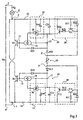
La figure 1 représente, de façon très schématique et
sous forme de blocs, un exemple classique de circuit 1 de
commande d'une charge Q alimentée par une tension alternative
Vac. Deux interrupteurs K1 et K2 sont montés en anti-parallèle
entre deux bornes 2 et 3 de puissance du gradateur, connecté en
série avec la charge Q entre deux bornes P et N d'application de
la tension alternative Vac. Chaque interrupteur K1, K2 a sa
borne de commande reliée en sortie d'un circuit 4 (DRIV1),
respectivement 5 (DRIV2), générant un signal de commande
approprié à partir de consignes de commande reçues d'un circuit
de commande commun (CTRL) 6. Le circuit 6 reçoit une consigne de
puissance à destination de la charge, par exemple, au moyen d'un
potentiomètre 7 ajustant une tension de consigne exploitée par
le circuit 6.Figure 1 shows, very schematically and
in the form of blocks, a classic example of
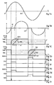
Les figures 2A à 2D illustrent le fonctionnement du gradateur de puissance de la figure 1 dont le principe est une commande par angle de phase. Les figures 2A à 2D représentent respectivement des exemples d'allures de la tension Vac, du courant IQ dans la charge Q, et des périodes de fermeture des interrupteurs K1 et K2.FIGS. 2A to 2D illustrate the operation of the power dimmer of FIG. 1, the principle of which is a control by phase angle. FIGS. 2A to 2D respectively represent examples of patterns of the voltage Vac, of the current I Q in the load Q, and of the periods of closure of the switches K1 and K2.
On suppose que la charge Q est une charge inductive, de sorte que son courant est déphasé par rapport à la tension alternative.We assume that the charge Q is an inductive charge, so that its current is out of phase with respect to the voltage alternative.
La commande par angle de phase consiste à contrôler l'instant de mise en conduction d'un des interrupteurs K1 ou K2 selon l'alternance considérée, à partir du début de l'alternance d'alimentation alternative. En fait, à chaque alternance, on commande l'instant t1, respectivement t2, de fermeture de l'interrupteur K1 ou K2 qui entraíne l'apparition d'un courant dans la charge. L'ouverture de l'interrupteur qui conduit (instant t1', t2', respectivement) est contrôlée par une détection de la disparition du courant IQ dans la charge, ce qui reproduit un fonctionnement de type triac. Comme on suppose une charge inductive, l'instant t1' respectivement t2' d'ouverture des interrupteurs et de disparition du courant dans la charge est décalé par rapport aux instants de passage par zéro de la tension alternative Vac.The phase angle control consists in controlling the instant of conduction of one of the switches K1 or K2 according to the alternation considered, from the start of the alternating supply alternation. In fact, at each half-cycle, the instant t1, respectively t2, of closure of the switch K1 or K2 is commanded, which causes the appearance of a current in the load. The opening of the switch which conducts (instant t1 ', t2', respectively) is controlled by a detection of the disappearance of the current I Q in the load, which reproduces a triac type operation. As an inductive load is assumed, the instant t1 'respectively t2' of opening of the switches and disappearance of the current in the load is offset with respect to the instants of zero crossing of the alternating voltage Vac.
Les contraintes que doit respecter un circuit de commande tel qu'illustré par la figure 1 sont de fournir les potentiels de référence aux électrodes de commande des interrupteurs semiconducteurs, de transférer l'information du circuit de commande 6 au circuit (ici 5) ne possédant pas la même référence de tension, et de détecter le passage par zéro du courant dans l'interrupteur conducteur.The constraints that a circuit of command as illustrated in Figure 1 are to provide the reference potentials for the control electrodes semiconductor switches, to transfer information from control circuit 6 to the circuit (here 5) not having the same voltage reference, and detect the zero crossing of the current in the conductor switch.
Dans les circuits classiques de ce type, le respect de ces contraintes impose le recours à deux alimentations externes indépendantes pour fournir les tensions Vcc1 et Vcc2, donc généralement un transformateur. De plus, le transfert de l'information pour l'étage (par exemple 5) ne possédant pas la même référence de tension que le circuit de commande 6 requiert une barrière d'isolement 8 (IB) de type optocoupleur, transformateur d'impulsions ou décaleur de niveau.In classic circuits of this type, respect for these constraints require the use of two external power supplies independent to supply the voltages Vcc1 and Vcc2, therefore usually a transformer. In addition, the transfer of information for the floor (for example 5) not having the same voltage reference as the control circuit 6 requires an isolation barrier 8 (IB) of optocoupler type, pulse transformer or level shifter.
En outre, la détection du zéro de tension requiert,
pour permettre une ouverture aux zéro de courant dans la charge
et éviter ainsi des surtensions néfastes à l'ouverture, que
chaque circuit 4, 5 ait une borne d'entrée reliée à une borne de
puissance du gradateur (respectivement, la borne 2 pour
l'interrupteur K1 et la borne 3 pour l'interrupteur K2). En
pratique, cela conduit généralement à prévoir une résistance
(non représentée) en série avec chacun des interrupteurs pour en
mesurer la tension. Une telle résistance engendre des pertes non
souhaitables lorsque l'interrupteur est à l'état passant.In addition, voltage zero detection requires,
to allow opening to zero current in the load
and thus avoid harmful overvoltages on opening, that
each
La présente invention vise à proposer un circuit de commande pour deux interrupteurs unidirectionnels en courant montés en anti-parallèle qui pallie les inconvénients des circuits classiques.The present invention aims to provide a circuit for control for two current unidirectional switches mounted in anti-parallel which overcomes the disadvantages of classic circuits.
L'invention vise plus particulièrement à proposer un circuit de commande qui ne nécessite pas la génération de tensions d'alimentation externes indépendantes.The invention aims more particularly to propose a control circuit which does not require the generation of independent external supply voltages.
L'invention vise également à proposer une solution qui ne requiert pas de barrière d'isolement pour transférer une consigne de commande.The invention also aims to propose a solution which does not require an isolation barrier to transfer a order instruction.
L'invention vise en outre à éviter la présence d'un shunt de courant (résistance, ou sonde à effet hall) en série avec chaque interrupteur pour détecter le zéro de courant dans la charge.The invention further aims to avoid the presence of a current shunt (resistor, or hall effect probe) in series with each switch to detect zero current in load.
L'invention vise également à proposer un circuit de commande réalisable sous forme de circuit intégré, et compatible avec la réalisation d'un interrupteur bidirectionnel sous forme de dipôle, comprenant deux interrupteurs unidirectionnels en courant et de leur circuit de commande. The invention also aims to propose a circuit for control achievable as an integrated circuit, and compatible with the realization of a bidirectional switch in the form dipole, comprising two unidirectional switches in current and their control circuit.
Pour atteindre ces objets et d'autres, la présente
invention prévoit un circuit de commande de deux interrupteurs
bidirectionnels en tension et unidirectionnels en courant,
montés en anti-parallèle, comportant en série entre deux bornes du
montage en anti-parallèle, deux étages de commande identiques
respectivement dédiés à chaque interrupteur et entre lesquels
est intercalée une impédance commune fixant un angle de phase de
fermeture des interrupteurs, chaque étage comportant :
Selon un mode de réalisation de la présente invention, ladite source de courant est dimensionnée pour contrôler le di/dt à la fermeture de l'interrupteur concerné.According to an embodiment of the present invention, said current source is sized to control the di / dt when the relevant switch is closed.
Selon un mode de réalisation de la présente invention, ledit montage de déchargement est activé dès l'annulation du courant dans l'interrupteur concerné.According to an embodiment of the present invention, said unloading arrangement is activated as soon as the current in the relevant switch.
Selon un mode de réalisation de la présente invention, le condensateur de chaque étage est en série avec une première diode, entre l'impédance et la borne de l'étage qui est confondue avec la borne du montage en anti-parallèle.According to an embodiment of the present invention, the capacitor of each stage is in series with a first diode, between the impedance and the terminal of the stage which is confused with the anti-parallel mounting terminal.
Selon un mode de réalisation de la présente invention, une deuxième diode de chaque étage relie ladite impédance à ladite borne de l'étage confondue avec la borne du montage en anti-parallèle.According to an embodiment of the present invention, a second diode of each stage connects said impedance to said terminal of the stage combined with the terminal of the mounting in antiparallel.
Selon un mode de réalisation de la présente invention, une troisième diode relie l'électrode de commande de l'interrupteur de chaque étage à l'électrode dudit condensateur, de telle sorte que ledit montage de déchargement décharge également l'électrode de commande de l'interrupteur de l'étage.According to an embodiment of the present invention, a third diode connects the control electrode the switch of each stage at the electrode of said capacitor, so that said discharge assembly discharges also the stage switch control electrode.
Selon un mode de réalisation de la présente invention, le condensateur respectif de chaque étage fournit l'alimentation nécessaire à tous les constituants de l'étage.According to an embodiment of the present invention, the respective capacitor of each stage supplies the power necessary for all the components of the floor.
Selon un mode de réalisation de la présente invention, ledit élément d'activation-désactivation active ladite source de courant à laquelle il est associé lorsque la tension aux bornes du condensateur de l'étage devient supérieure à un premier seuil, lui-même supérieur à la tension seuil de l'interrupteur concerné.According to an embodiment of the present invention, said activation-deactivation element activates said source of current to which it is associated when the terminal voltage of the stage capacitor becomes greater than a prime threshold, itself higher than the voltage threshold of the switch concerned.
Selon un mode de réalisation de la présente invention, ledit comparateur désactive ladite source de courant à laquelle il est associé lorsque la tension aux bornes du condensateur de l'étage devient supérieure à un deuxième seuil, lui-même de préférence inférieur à ladite tension seuil de l'interrupteur concerné.According to an embodiment of the present invention, said comparator deactivates said current source at which it is associated when the voltage across the capacitor of the floor becomes higher than a second threshold, itself of preferably lower than said switch threshold voltage concerned.
Selon un mode de réalisation de la présente invention, chaque montage de déchargement comporte un premier transistor en parallèle sur le condensateur de l'étage, l'électrode de commande du premier transistor étant reliée, par l'intermédiaire d'un deuxième transistor, à ladite impédance.According to an embodiment of the present invention, each unloading assembly comprises a first transistor in parallel on the stage capacitor, the electrode control of the first transistor being connected, via a second transistor, at said impedance.
Selon un mode de réalisation de la présente invention, ledit élément d'activation-désactivation de chaque étage est constitué d'un comparateur recevant sur une première entrée la tension aux bornes du condensateur de l'étage et sur une deuxième entrée une tension de référence, ledit comparateur étant alimenté par la tension aux bornes du condensateur de l'étage concerné.According to an embodiment of the present invention, said activation-deactivation element of each stage is consisting of a comparator receiving on a first input the voltage across the stage capacitor and on a second input a reference voltage, said comparator being supplied by the voltage across the capacitor of the floor concerned.
Selon un mode de réalisation de la présente invention, ladite impédance est constituée d'un potentiomètre.According to an embodiment of the present invention, said impedance consists of a potentiometer.
Selon un mode de réalisation de la présente invention, ladite impédance est constituée d'une première résistance en parallèle avec une deuxième résistance commutable, ladite première résistance étant de valeur nettement supérieure à la seconde.According to an embodiment of the present invention, said impedance consists of a first resistance in parallel with a second switchable resistor, said first resistance being of value clearly higher than the second.
L'invention prévoit également un gradateur de puissance d'une charge.The invention also provides a dimmer for load power.
L'invention prévoit également un circuit de commande d'un moteur.The invention also provides a control circuit of an engine.
Ces objets, caractéristiques et avantages, ainsi que
d'autres de la présente invention seront exposés en détail dans
la description suivante de modes de réalisation particuliers
faite à titre non-limitatif en relation avec les figures jointes
parmi lesquelles :
Les mêmes éléments ont été désignés par les mêmes références aux différentes figures. Pour des raisons de clarté, seuls les éléments qui sont nécessaires à la compréhension de l'invention ont été représentés aux figures et seront décrits par la suite. En particulier, la charge commandable par le circuit de l'invention n'a pas été détaillée, celle-ci s'appliquant quelle que soit la charge résistive et/ou inductive à commander par une tension alternative d'alimentation et dont on souhaite moduler la puissance de fonctionnement en fonction d'une consigne.The same elements have been designated by the same references to the various figures. For reasons of clarity, only the elements that are necessary for the understanding of the invention have been shown in the figures and will be described thereafter. In particular, the load controllable by the circuit of the invention has not been detailed, it applicable regardless of the resistive and / or inductive load to be controlled by an AC supply voltage and of which we want to modulate the operating power as a function a deposit.
La figure 3 représente un mode de réalisation d'un circuit de commande de deux interrupteurs selon l'invention.FIG. 3 represents an embodiment of a control circuit of two switches according to the invention.
Comme précédemment, deux interrupteurs K1 et K2
unidirectionnels en courant sont connectés en anti-parallèle
entre deux bornes 2 et 3 définissant un interrupteur
bidirectionnel en tension et en courant, monté en série avec une
charge Q entre deux bornes P et N d'application d'une tension
alternative Vac. Dans l'exemple de la figure 3, on suppose que
les interrupteurs K1 et K2 sont des composants semiconducteurs
de type MBS, également appelés RGIGBT. Comme cela sera détaillé
en relation avec la figure 5A, de tels interrupteurs reprennent
le fonctionnement d'un transistor IGBT en intégrant une diode de
protection, ce qui les rend bidirectionnels en tension. Cette
diode est symbolisée par un trait sur le collecteur de
l'interrupteur.As before, two switches K1 and K2
unidirectional current are connected in anti-parallel
between two
Selon l'invention, chaque interrupteur K1, K2 est
associé à un étage de commande 10, 20 qui lui est dédié. Les
étages 10 et 20 sont identiques et sont reliés l'un à l'autre
par une impédance commune 30 fixant l'angle de phase de
fermeture des interrupteurs. En figure 3, l'impédance commune
est constituée d'un potentiomètre 30 dont les deux bornes sont
respectivement reliées aux étages 10 et 20. Chaque étage 10, 20
a une structure tripolaire, c'est-à-dire qu'il comprend deux
bornes 11 et 12, respectivement 21 et 22, connectées entre
l'impédance commune 30 et l'émetteur du transistor MBS K1,
respectivement K2, et une borne de sortie 13, respectivement 23,
de commande de l'interrupteur K1, respectivement K2. On voit
déjà apparaítre une différence par rapport au circuit de
commande classique de la figure 1 pour lequel les étages
affectés aux interrupteurs respectifs requièrent cinq bornes. According to the invention, each switch K1, K2 is
associated with a
La structure d'un étage de commande selon l'invention
sera décrite par la suite en relation avec l'étage 10 de
commande de l'interrupteur K1. L'étage 20 de commande de
l'interrupteur K2 présente exactement la même structure et ses
constituants sont référencés en figure 3 par des références
commençant par le chiffre 2 et non par le chiffre 1.The structure of a control stage according to the invention
will be described later in relation to stage 10 of
control of switch K1. The
L'étage 10 comporte une source de courant 14
commandable dont la sortie est reliée à la borne 13 de commande
de l'interrupteur K1 et qui est destinée à commander sa
fermeture. Par exemple, la source de courant 14 est une source
de courant constant commandée par un élément 15 d'activation-désactivation.
Selon l'invention, l'élément 15 active la source
de courant 14 en fonction de la tension aux bornes d'un
condensateur C11 fonctionnellement en série avec le
potentiomètre 30 entre les bornes 2 et 3 de l'interrupteur,
l'impédance du potentiomètre 30 conditionnant donc l'angle de
phase de fermeture de l'interrupteur K1.
Dans l'exemple de la figure 3, l'élément d'activation-désactivation
de la source de courant est constitué d'un
comparateur 16 à hystérésis dont une première entrée est reliée
à l'électrode du condensateur C11 opposée à la borne 3 et dont
une deuxième entrée reçoit une tension de référence Vref
fournie, par exemple, par une diode Zener ou un circuit de
génération d'une référence de tension de type Bandgap.In the example in Figure 3, the activation-deactivation element
of the current source consists of a
Selon l'invention, le condensateur C11 a également le
rôle d'alimenter l'étage 10 pendant les alternances (par
exemple, positives) affectées à cet étage 10. Ainsi, ce
condensateur C11 fournit la tension d'alimentation de la source
de courant 14 lui permettant d'activer l'interrupteur K1 ainsi
que la tension d'alimentation de l'élément d'activation-désactivation
(plus particulièrement du comparateur 16) dont les
bornes d'alimentation respectives sont connectées aux bornes 17
et 12 du condensateur C11.According to the invention, the capacitor C11 also has the
role of supplying
Pour affecter l'étage 10 à un seul type d'alternances,
ici les alternances positives, une diode D12 relie la borne 11
de l'impédance 30 à l'électrode 17 du condensateur. Cette diode
D12 dont l'anode est connectée à la borne 11 n'est polarisée en
direct que pendant les alternances positives. Pour permettre la
circulation du courant malgré la présence de la diode (D22)
associée à l'étage 20, une diode D21 de cet étage 20 court-circuite
ses bornes 21 et 22 pendant les alternances positives,
l'anode de la diode D21 étant connectée à la borne 22. Côté
étage 10, une diode D11 est connectée entre les bornes 11 et 12,
son anode étant connectée à la borne 12.To assign
Selon l'invention, l'étage 10 comporte également un
montage 18 de déchargement du condensateur C11 pendant
l'alternance où cet étage n'est pas conducteur, afin de
réinitialiser l'étage en préparation de l'alternance positive
suivante. Pendant cette décharge, il est également nécessaire de
décharger la grille de l'interrupteur K1 si celui-ci est du type
à grille isolée. Pour cela, on relie alors la borne 13 à
l'électrode 17 du condensateur C11 par une diode D13 dont
l'anode est connectée à la borne 13. Ainsi, on déchargera la
grille de l'interrupteur K1 en même temps que le condensateur
C11.According to the invention,
Dans l'exemple de la figure 3, le montage 18 est
constitué d'un premier transistor bipolaire de type PNP T12
connecté entre les électrodes 17 et 12 du condensateur C11, son
émetteur étant connecté à l'électrode 17. La base du transistor
T12 est connectée, de préférence par l'intermédiaire d'une
résistance de polarisation R12, au collecteur d'un transistor
bipolaire de type NPN T11 dont l'émetteur est connecté à la
borne 11, c'est-à-dire à l'extérieur de l'étage 10 pour
permettre une conduction pendant les alternances de signe
opposé. La base du transistor T11 est connectée, de préférence
par l'intermédiaire d'une résistance de polarisation R11, à la
borne 12 de l'étage 10.In the example of FIG. 3, the
On voit déjà que le circuit de commande de l'invention, dans sa version telle qu'illustrée par la figure 3 où l'élément de commande est un potentiomètre, se présente sous la forme d'un dipôle complètement autonome.We can already see that the control circuit of the invention, in its version as illustrated by FIG. 3 where the control element is a potentiometer, is found under the shape of a completely autonomous dipole.
Les figures 4A à 4J illustrent, par des chronogrammes,
le fonctionnement du circuit de la figure 3. Ces chronogrammes
représentent respectivement des exemples d'allures des signaux
Vac, IQ, VC11 et V13 représentant respectivement la tension aux
bornes du condensateur C11 et la tension de polarisation de la
grille de l'interrupteur K1, VC21 et V23 représentant
respectivement la tension aux bornes du condensateur C21 et la
tension de grille de l'interrupteur K2, les périodes de
conduction du circuit 18 et de la diode D11, les périodes de
conduction de la diode D12, les périodes de conduction de la
diode D13, les périodes de conduction du circuit 28 et de la
diode D21, les périodes de conduction de la diode D22, et les
périodes de conduction de la diode D23.FIGS. 4A to 4J illustrate, by timing diagrams, the operation of the circuit of FIG. 3. These timing diagrams respectively represent examples of patterns of the signals Vac, I Q , VC11 and V13 respectively representing the voltage across the terminals of the capacitor C11 and the bias voltage of the gate of the switch K1, VC21 and V23 representing respectively the voltage across the capacitor C21 and the gate voltage of the switch K2, the conduction periods of the
Les figures 4A à 4J illustrent le fonctionnement du circuit pour commander une charge Q purement résistive. Un autre exemple appliqué à une charge inductive (ou résistive et inductive) sera décrit plus loin en relation avec les figures 7A à 7J.FIGS. 4A to 4J illustrate the operation of the circuit for controlling a purely resistive load Q. Another example applied to an inductive (or resistive and inductive) will be described later in relation to FIGS. 7A at 7J.
Initialement, les condensateurs C11 et C12 sont déchargés et toutes les diodes et transistors sont bloqués. On suppose qu'à un instant t0, on applique la tension alternative Vac aux bornes du système et on suppose, pour simplifier la description, que cet instant correspond au début d'une alternance positive. De la description qui suit, il ressortira toutefois que l'instant de mise sous tension n'a pas d'incidence néfaste sur le fonctionnement. Pour simplifier, on ne tiendra pas compte des chutes de tension en direct des différentes diodes (généralement de l'ordre de 0,6 volts) lorsqu'elles n'ont pas d'influence sur le fonctionnement du circuit.Initially, capacitors C11 and C12 are discharged and all diodes and transistors are blocked. We suppose that at an instant t0, the alternating voltage is applied Vac across the system and we assume, to simplify the description, that this instant corresponds to the beginning of a positive alternation. From the description which follows, it will emerge however, the instant of power-up does not affect detrimental to the operation. To simplify, we will not not account for direct voltage drops from different diodes (usually around 0.6 volts) when they are not no influence on the functioning of the circuit.
Dès le début de l'alternance positive (à partir de
l'instant t0), les diodes D21 et D12 se trouvent polarisées en
direct (figure 4F et figure 4H), tandis que les diodes D22 et
D11 sont bloquées (figure 4E et figure 4I) . Par ailleurs, comme
la diode D21 est passante, l'étage 28 conduit également. Pour
l'instant, on se contente de noter que le fait que cet étage
conduit force un blocage de l'interrupteur K2 et une décharge du
condensateur C22. Le fonctionnement du montage de déchargement
sera détaillé plus loin en relation avec le fonctionnement de
l'étage 10. De même, les transistors T11 et T12 du montage 18
sont tous deux bloqués dans la mesure où la diode D11 est
bloquée. Il en découle que la diode D13 est bloquée dans la
mesure où on suppose un potentiel initialement bas (potentiel de
la borne 12) pour la grille de l'interrupteur K1.From the start of the positive changeover (from
at time t0), the diodes D21 and D12 are polarized at
direct (Figure 4F and Figure 4H), while diodes D22 and
D11 are blocked (Figure 4E and Figure 4I). By the way, as
diode D21 is conducting,
Un courant de charge du condensateur C11 circule donc
depuis la borne 2 vers la borne 3 à travers la diode 21, le
potentiomètre 30 et la diode D12. La rapidité avec laquelle se
charge le condensateur C11 (figure 4C) dépend de la résistance
de l'élément 30. Le condensateur C11 et la plage de variation de
la résistance 30 sont dimensionnés pour que la tension aux
bornes du condensateur C11 soit suffisante pour alimenter le
comparateur 16 et la source de courant 14. La constitution de la
source 14 pourra être quelconque pourvu d'être commandable. Par
exemple, il pourra s'agir d'une source de courant réalisée à
partir d'un miroir de courant en transistors MOS, alimenté par
la tension aux bornes du condensateur C11.A charging current of the capacitor C11 therefore flows
from
A un instant t3, la tension aux bornes du condensateur
C1 atteint la tension de référence Vref du comparateur 16. Il en
découle une commutation de ce comparateur, ce qui active la
source de courant 14. En supposant un courant constant fourni
par la source 14, le potentiel de la grille 13 de l'interrupteur
K1 se met à croítre à partir de l'instant t3 et sa croissance se
poursuit jusqu'à rejoindre, à un instant t4, le potentiel de la
borne 17, c'est-à-dire la tension VC11. A partir de l'instant
t4, la tension de grille V13 de l'interrupteur K1 suit l'allure
de la tension VC11 aux bornes du condensateur C11.At an instant t3, the voltage across the capacitor
C1 reaches the reference voltage Vref of
Entre les instants t3 et t4, dès que la tension V13
atteint la tension seuil Vth de l'interrupteur K1 (instant t5),
celui-ci devient conducteur et un courant commence à circuler
dans la charge Q par l'intermédiaire de l'interrupteur K1
(figure 4B). La croissance du courant IQ dans la charge
s'effectue sans pic grâce à la source de courant 14 qui contrôle
di/dt à la fermeture de l'interrupteur K1. On suppose qu'à un
instant t6, le courant IQ dans la charge a rejoint l'allure de
la tension alternative Vac, l'interrupteur K1 ayant atteint sa
zone de fonctionnement saturée.Between instants t3 and t4, as soon as the voltage V13 reaches the threshold voltage Vth of the switch K1 (instant t5), the latter becomes conductive and a current begins to flow in the load Q via the switch K1 (Figure 4B). The growth of the current I Q in the load is carried out without peak thanks to the
Selon l'invention, pour que cette condition soit
respectée, la tension Vref (plus précisément, le niveau de
commutation du comparateur 16 dans le sens croissant de la
tension du condensateur C11) est choisie pour être nettement
supérieure à la tension seuil Vth de l'interrupteur K1.According to the invention, for this condition to be
respected, the voltage Vref (more precisely, the level of
switching of
A l'instant t6 où l'interrupteur K1 est pleinement
passant, les bornes 2 et 3 du circuit de commande se trouvent
court-circuitées, ce qui entraíne le blocage des diodes D21 et
D12 et, par voie de conséquence, de l'étage 28.At time t6 when the switch K1 is fully
passing,
L'étage 10 est alors isolé de l'alimentation
alternative et de la charge. Par conséquent, le condensateur C11
ne se décharge pas. Dans l'exemple de la figure 3,
l'interrupteur K1 est un MBS, c'est-à-dire un composant à grille
isolée. La décharge du condensateur C11 liée à la commande de
grille de cet interrupteur est donc négligeable.
A l'instant t10 où l'alternance positive de la tension
Vac s'annule, il ne se passe rien. En effet, bien que l'on ait
négligé les chutes de tension dans les différentes diodes, il
faut attendre le début de l'alternance négative pour que les
diodes D11 et D22 deviennent conductrices et qu'un courant
circule alors dans le circuit de commande et dans le
potentiomètre 30 pour charger le condensateur C22 pendant cette
alternance négative. Côté étage 20, on reproduit pendant
l'alternance négative le fonctionnement exposé ci-dessus en
relation avec l'alternance positive.At time t10 when the positive alternation of the voltage
Vac is canceled, nothing happens. Indeed, although we have
neglected the voltage drops in the different diodes it
must wait for the start of the negative alternation so that the
diodes D11 and D22 become conductive and that a current
then circulates in the control circuit and in the
Côté étage 10, la conduction de la diode D11 provoque
l'activation du montage 18 de déchargement du condensateur C1.
En fait, la conduction de la diode D11 rend le transistor T11
conducteur et la différence de potentiel existante aux bornes du
condensateur C11 permet la mise en conduction du transistor T12
qui provoque alors la décharge du condensateur C11. De plus,
comme la grille de l'interrupteur K1 est initialement au
potentiel V13, identique à la tension aux bornes du condensateur
C11, la diode D13 se trouve polarisée en direct, ce qui permet
la décharge de la grille de l'interrupteur 13 pour préparer
celui-ci pour l'alternance suivante.Side of
En fait, le condensateur C11 se décharge peu après le
début de l'alternance négative, c'est-à-dire dès que la diode
D11 conduit. En d'autres termes, dès que la tension entre les
bornes 2 et 3 du circuit de commande devient supérieur à -2*Vf,
où Vf représente la chute de tension d'une diode en direct, ici
- (VfD11+VfD22) où VfD11 et VfD22 représentent les chutes de
tension en direct respectives des diodes D11 et D22. Lors de
l'ouverture de l'interrupteur K1, il ne se produit pas de pic de
courant dans la mesure où l'ouverture intervient alors que la
tension aux bornes du commutateur est négative.In fact, the capacitor C11 discharges soon after the start of the negative half-wave, that is to say as soon as the diode D11 conducts. In other words, as soon as the voltage between
Aux figures 4, on a considéré que le condensateur C11
se trouvait intégralement déchargé à un instant t17. A partir de
cet instant, la diode D13 se bloque, la grille de l'interrupteur
K11 étant déchargée. Lors de la décharge du condensateur C11, le
comparateur 16 commute pour éteindre la source de courant 14,
avant que ce condensateur C11 soit intégralement déchargé.In FIGS. 4, it has been considered that the capacitor C11
was fully discharged at time t17. From
this instant, the diode D13 is blocked, the grid of the switch
K11 being discharged. When discharging the capacitor C11, the
Le seuil de commutation bas (tension VC11
décroissante) du comparateur 16 est, de préférence, inférieur à
la tension seuil Vth de l'interrupteur K1 pour des raisons de
stabilité à l'ouverture de la source de courant. Par conséquent,
l'hystérésis du comparateur 16 est choisie pour que le seuil Vth
soit compris entre le seuil Vref de commutation dans le sens
croissant et le seuil de commutation dans le sens décroissant.The low switching threshold (voltage VC11
decreasing) of
En fin d'alternance négative, on assiste de nouveau à
une conduction de l'étage de commande 10. Celui-ci redémarre
comme dans l'état initial décrit précédemment dans la mesure où
tous ses composants se sont trouvés déchargés par la décharge du
condensateur C11. La seule différence est que la diode 23
devient conductrice au début de la deuxième alternance positive
alors qu'elle ne l'était pas lors de la première alternance car
on avait considéré un état initial non alimenté du circuit.At the end of negative alternation, we again witness
conduction of the
Une variation de la résistance 30 a pour effet de
modifier l'aspect de charge des condensateurs C11 et C22 selon
les alternances et, par voie de conséquence, les instants t3 et
t13 de début de conduction des commutateurs K1 et K2 à chaque
alternance.A variation of the
Un avantage de la présente invention est que le circuit de commande ne nécessite aucun circuit d'alimentation externe et notamment aucun transformateur.An advantage of the present invention is that the control circuit requires no power circuit external and in particular no transformer.
Un autre avantage de la présente invention est que la détection du zéro de courant effectuée par lecture de la tension inverse évite l'apparition de surtensions lors de l'ouverture des commutateurs sur charge inductive.Another advantage of the present invention is that the current zero detection by reading the voltage reverse prevents the appearance of overvoltages during opening switches on inductive load.
Un autre avantage de l'invention est que le di/dt à la
fermeture des commutateurs est contrôlé par la source de courant
14.Another advantage of the invention is that the di / dt at the
closing of the switches is controlled by the
Un autre avantage de l'invention est qu'elle ne requiert aucune barrière d'isolement pour assurer la commande de l'un ou l'autre des étages.Another advantage of the invention is that it does not requires no isolation barrier to control either floor.
D'autres avantages de l'invention résident dans la simplicité du circuit de commande et dans la symétrie de la commande réalisée quel que soit le signe de l'alternance.Other advantages of the invention lie in the simplicity of the control circuit and in the symmetry of the command carried out whatever the sign of alternation.
Un autre avantage de l'invention est que le circuit de
commande proposé est entièrement intégrable (à l'exception
néanmoins du potentiomètre de commande). En effet, comme il
ressort du fonctionnement décrit ci-dessus, aucune des diodes du
circuit de commande (notamment les diodes D11, D12, D21 et D22)
n'a besoin de tenir une tension élevée. En effet, les seules
périodes (instants t6 à t10 et t16 à t0) pendant lesquelles le
courant circulant dans le circuit de commande n'est pas absorbé
par le potentiomètre 30, sont les périodes où l'un des
interrupteurs K1 ou K2 est pleinement conducteur (saturé), d'où
il résulte que les bornes 2 et 3 sont court-circuitées.Another advantage of the invention is that the circuit for
proposed order is fully integrable (except
control potentiometer). Indeed, as it
spring of the operation described above, none of the diodes of the
control circuit (in particular diodes D11, D12, D21 and D22)
does not need to hold a high voltage. Indeed, the only
periods (instants t6 to t10 and t16 to t0) during which the
current flowing in the control circuit is not absorbed
by
Un autre avantage de la présente invention est que le gradateur de puissance ainsi constitué ne requiert ni inductance, ni condensateur de filtrage, ni alimentation externe. L'invention est donc parfaitement compatible avec la réalisation d'un gradateur sous la forme d'un dipôle.Another advantage of the present invention is that the power dimmer thus formed does not require inductor, neither filter capacitor, nor power supply external. The invention is therefore perfectly compatible with the realization of a dimmer in the form of a dipole.
Les figures 5A à 5D illustrent des exemples de
commutateurs K1 ou K2 susceptibles d'être utilisés dans un
circuit de commande selon l'invention. La figure 5A représente
le schéma d'un transistor de type MBS 40 tel que représenté en
relation avec la figure 3. Un tel composant présente l'avantage
d'être unidirectionnel en courant tout en étant bidirectionnel
en tension, c'est-à-dire tenant la tension inverse grâce à une
diode intégrée, symbolisée par un trait 41 en figure 5A. Il en
découle que la chute de tension à l'état passant est limitée à
la tension collecteur-émetteur de saturation VCEsat du
composant.FIGS. 5A to 5D illustrate examples of
switches K1 or K2 capable of being used in a
control circuit according to the invention. Figure 5A shows
the diagram of an
La figure 5B illustre un deuxième exemple de
commutateur 42 constitué d'un transistor IGBT 43 en série avec
une diode 44. Le schéma de la figure 5B constitue un équivalent
du transistor MBS 40 de la figure 5A mais dans lequel la chute
de tension à l'état passant correspond à la somme de la tension
VCEsat du transistor IGBT 43 et de la tension VF de la diode 44
en direct.FIG. 5B illustrates a second example of a
La figure 5C représente un troisième exemple
d'interrupteur 45, constitué ici d'un transistor MOS 46 en série
avec une diode 47.Figure 5C shows a
La figure 5D illustre un quatrième exemple de
commutateur 48 constitué d'un transistor bipolaire de type NPN
49 en série avec une diode 50.Figure 5D illustrates a fourth example of
Toute structure de commutateur unidirectionnel en
courant et bidirectionnel en tension (même si le caractère
bidirectionnel en tension est apporté par une diode distincte
introduisant une chute de tension supplémentaire) peut être
utilisée. La seule précaution éventuelle est, dans le cas d'un
transistor bipolaire (figure 5D) ou plus généralement d'un
interrupteur à commande en courant, de prévoir un condensateur
C11 de capacité suffisante pour assurer la fourniture du courant
de base au transistor 49 pendant toute sa période de conduction,
tout en maintenant l'alimentation du comparateur 16 et de la
source de courant 14. Dans le cas où il n'est pas indispensable
de décharger l'électrode de commande de l'interrupteur, la diode
D13 (ou D23) peut être omise.Any unidirectional switch structure in
current and bidirectional in voltage (even if the character
bidirectional in voltage is provided by a separate diode
introducing an additional voltage drop) may be
used. The only possible precaution is, in the case of a
bipolar transistor (Figure 5D) or more generally of a
current control switch, to provide a capacitor
C11 of sufficient capacity to supply electricity
basic to
La figure 6 représente un deuxième mode de réalisation
d'un élément 60 constituant une impédance commune entre les
étages 10 et 20 de la figure 3. Ce mode de réalisation est
destiné à permettre une commande du gradateur de puissance par
un signal CTRL externe au gradateur de puissance proprement dit.FIG. 6 represents a second embodiment
of an
Selon ce mode de réalisation, l'impédance 60 comporte,
en parallèle entre ses bornes 21 et 11, une résistance Rp de
protection et une association en série d'une résistance Rc et
d'un commutateur K commandé par le signal externe CTRL. Le rôle
de la résistance Rc est de limiter le courant dans les diodes
D12, D21 et D22, D11 respectivement, lorsque l'interrupteur K
est fermé. Cela permet d'autoriser une fermeture de
l'interrupteur K à n'importe quel instant par rapport à la
tension d'alimentation Vac. Le rôle de la résistance Rp est de
garantir une ouverture automatique au zéro de courant même si
l'interrupteur K s'est trouvé ouvert entre temps sous l'effet
d'une disparition du signal CTRL. On veillera à choisir une
résistance Rp nettement plus importante que la résistance Rc
afin de permettre une circulation du courant dans la branche de
résistance Rc lorsque l'interrupteur est fermé. De plus, la
résistance Rp devra être d'une valeur suffisamment grande pour
que la charge des condensateurs C11 et C21 ne puisse pas
atteindre le niveau Vref en une demi-période d'alimentation
alternative lorsque l'interrupteur K est ouvert.According to this embodiment, the
Les figures 7A à 7J illustrent, par des chronogrammes représentant les mêmes signaux que les figures 4A à 4J, le fonctionnement d'un circuit de commande selon l'invention, connecté à une charge Q au moins partiellement inductive. La différence principale par rapport aux chronogrammes des figures 4A à 4J est que l'allure du courant IQ dans la charge a une croissance dont le di/dt est limité naturellement par l'inductance de la charge.Figures 7A to 7J illustrate, by timing diagrams representing the same signals as Figures 4A to 4J, the operation of a control circuit according to the invention, connected to a load Q at least partially inductive. The main difference compared to the timing diagrams of FIGS. 4A to 4J is that the shape of the current I Q in the load has a growth whose di / dt is naturally limited by the inductance of the load.
Une autre différence est qu'en raison du déphasage
apporté par l'inductance de la charge sur les instants (t0',
t10', figure 7B) d'annulation du courant dans celle-ci par
rapport aux instants de passage par zéro (t0, t10, figure 7A) de
la tension Vac, la charge du condensateur C11 ou C21 s'effectue
plus rapidement. Il en découle que l'instant t3 de début de
fonctionnement de la source de courant 14 est plus près de
l'instant t0' qu'il ne l'est de l'instant t0 dans une charge
purement résistive.Another difference is that due to the phase shift
brought by the inductance of the load on the instants (t0 ',
t10 ', Figure 7B) cancellation of the current therein by
compared to the zero crossing instants (t0, t10, FIG. 7A) of
Vac voltage, the capacitor C11 or C21 is charged
faster. It follows that the instant t3 of the start of
operation of
Pour le reste, le fonctionnement du circuit de commande se déduit de l'exposé effectué précédemment en relation avec une charge résistive.For the rest, the functioning of the order is deduced from the presentation made previously in relation with a resistive load.
On notera que même sur une charge inductive, l'invention ne nécessite pas de shunt en série avec la charge pour détecter le passage par zéro du courant dans la charge. Selon l'invention, on utilise le déphasage lié à la charge inductive pour garantir une ouverture des commutateurs à un moment où la tension à leurs bornes est négative. Cela induit une détection naturelle du zéro de courant. Un avantage est alors que l'on évite les sur-tensions à l'ouverture des commutateurs de type thyristor. Un autre avantage est que cela réduit les pertes liées à la résistance de shunt, en série avec le commutateur, dans les circuits classiques.Note that even on an inductive load, the invention does not require a shunt in series with the load to detect the zero crossing of the current in the load. According to the invention, the phase shift linked to the load is used inductive to guarantee an opening of the switches to a when the voltage across their terminals is negative. This induces natural zero current detection. An advantage is while avoiding over-voltages when opening thyristor type switches. Another advantage is that reduces shunt resistance losses, in series with the switch, in conventional circuits.
L'impédance de commande de l'invention intervient sur
une charge inductive comme pour une charge résistive afin de
contrôler la charge du condensateur C11 ou C21 selon
l'alternance, donc l'intervalle entre les instants t'0 et t3 et
t'10 et t13 respectivement. Comme une fois le condensateur
chargé et le comparateur 16 déclenché, la commande de
l'interrupteur est fixée par la source de courant 14 dont le
fonctionnement est indépendant de l'impédance 30, la fixation de
l'instant t3 revient bien à fixer l'instant t5 de début de
conduction de la charge.The command impedance of the invention occurs on
an inductive load as for a resistive load in order to
check the charge of capacitor C11 or C21 according to
the alternation, therefore the interval between the instants t'0 and t3 and
t'10 and t13 respectively. Like once the capacitor
loaded and
Bien entendu, la présente invention est susceptible de diverses variantes et modifications qui apparaítront à l'homme de l'art. En particulier, la réalisation pratique des sources de courant et des comparateurs est à la portée de l'homme du métier à partir des indications fonctionnelles données ci-dessus. On rappellera toutefois que ces constituants ne nécessitent pas d'alimentation distincte de celle apportée par les condensateurs C1 et C21 prévus par le circuit de l'invention.Of course, the present invention is capable of various variations and modifications that will appear to humans art. In particular, the practical realization of the sources of current and comparators is within the reach of the skilled person from the functional indications given above. We remember, however, that these constituents do not require distinct from that provided by capacitors C1 and C21 provided by the circuit of the invention.
De plus, les dimensionnements des condensateurs et résistances, ainsi que des composants semiconducteurs est à la portée de l'homme du métier en fonction de l'application et du fonctionnement souhaité.In addition, the sizing of the capacitors and resistors as well as semiconductor components is at the scope of the skilled person depending on the application and desired operation.
En outre, on notera que l'invention peut réaliser un gradateur de puissance non seulement pour des circuits de type lampe, mais également pour assurer la commande de moteurs grâce à son fonctionnement performant sur charge inductive.In addition, it should be noted that the invention can achieve a power dimmer not only for type circuits lamp, but also to control motors with to its efficient operation on inductive load.
Enfin, bien que selon un mode de réalisation préféré,
l'invention prévoit un fonctionnement symétrique avec des
tensions Vref identiques pour le comparateur 16 et pour le
comparateur 26, elle n'exclut pas une dissymétrie selon
l'alternance positive ou négative, simplement en modifiant les
tensions Vref utilisées.Finally, although according to a preferred embodiment,
the invention provides for symmetrical operation with
identical Vref voltages for
Claims (15)
Applications Claiming Priority (2)
| Application Number | Priority Date | Filing Date | Title |
|---|---|---|---|
| FR0213685 | 2002-10-31 | ||
| FR0213685A FR2846807A1 (en) | 2002-10-31 | 2002-10-31 | CONTROL CIRCUIT FOR TWO CURRENT UNIDIRECTIONAL SWITCHES |
Publications (1)
| Publication Number | Publication Date |
|---|---|
| EP1416620A1 true EP1416620A1 (en) | 2004-05-06 |
Family
ID=32088428
Family Applications (1)
| Application Number | Title | Priority Date | Filing Date |
|---|---|---|---|
| EP03300167A Withdrawn EP1416620A1 (en) | 2002-10-31 | 2003-10-17 | Driver circuit for two unidirectional current switches |
Country Status (3)
| Country | Link |
|---|---|
| US (1) | US6900601B2 (en) |
| EP (1) | EP1416620A1 (en) |
| FR (1) | FR2846807A1 (en) |
Cited By (1)
| Publication number | Priority date | Publication date | Assignee | Title |
|---|---|---|---|---|
| FR2872354A1 (en) * | 2004-06-24 | 2005-12-30 | St Microelectronics Sa | POWER VARIATOR |
Families Citing this family (8)
| Publication number | Priority date | Publication date | Assignee | Title |
|---|---|---|---|---|
| FR2859580B1 (en) * | 2003-09-04 | 2006-01-21 | St Microelectronics Sa | DIMMER FOR RESISTIVE OR CAPACITIVE LOADS |
| US20070216375A1 (en) * | 2005-06-24 | 2007-09-20 | Stmicroelectronics S.A. | Power dimmer |
| FR2876515A1 (en) * | 2004-10-08 | 2006-04-14 | St Microelectronics Sa | DOUBLE POWER SUPPLY CIRCUIT |
| TW200806084A (en) * | 2005-12-12 | 2008-01-16 | Clipsal Australia Pty Ltd | Current zero crossing detector in a dimmer circuit |
| ES2334738B1 (en) | 2008-02-20 | 2010-10-27 | Simon Tech S.L. | DETECTION DEVICE DEVICE BY ZERO OF ALTERNATE ELECTRICAL CURRENT. |
| US8587266B2 (en) * | 2011-04-06 | 2013-11-19 | Tai-Her Yang | Synchronous regulation circuit for turn-on and turn-off phase angle of the AC voltage |
| FR2982721B1 (en) * | 2011-11-15 | 2013-11-29 | St Microelectronics Tours Sas | POWER VARIATOR |
| FR3104853B1 (en) * | 2019-12-13 | 2022-08-19 | Commissariat Energie Atomique | Switch control |
Citations (6)
| Publication number | Priority date | Publication date | Assignee | Title |
|---|---|---|---|---|
| US3878451A (en) * | 1972-12-08 | 1975-04-15 | Asea Ab | Thyristor circuit |
| US5796599A (en) * | 1997-03-12 | 1998-08-18 | Reliance Electric Industrial Company | Self-powered gate driver board |
| AU721986B2 (en) * | 1996-03-08 | 2000-07-20 | H.P.M. Industries Pty Limited | Controlled switching device |
| US6208126B1 (en) * | 1998-11-27 | 2001-03-27 | Stmicroelectronics S.A. | Circuit having a bidirectional switch for supplying a load from an AC voltage supply |
| US6255806B1 (en) * | 1998-03-23 | 2001-07-03 | Abb Ab | Supply device for power supply to an electronic unit in a semiconductor valve in a shunt-connected thyristor-switched capacitor |
| US20020047535A1 (en) * | 2000-06-16 | 2002-04-25 | Laurent Moindron | Bidirectional flip-flop |
Family Cites Families (2)
| Publication number | Priority date | Publication date | Assignee | Title |
|---|---|---|---|---|
| US4933798A (en) * | 1987-10-22 | 1990-06-12 | Widmayer R&D Ventures | Self protecting and automatic resetting capacitor synchronous switch apparatus for control of AC power to inductive loads |
| TW294669B (en) * | 1992-06-27 | 1997-01-01 | Hoechst Ag |
-
2002
- 2002-10-31 FR FR0213685A patent/FR2846807A1/en not_active Withdrawn
-
2003
- 2003-10-17 EP EP03300167A patent/EP1416620A1/en not_active Withdrawn
- 2003-10-31 US US10/698,809 patent/US6900601B2/en not_active Expired - Lifetime
Patent Citations (6)
| Publication number | Priority date | Publication date | Assignee | Title |
|---|---|---|---|---|
| US3878451A (en) * | 1972-12-08 | 1975-04-15 | Asea Ab | Thyristor circuit |
| AU721986B2 (en) * | 1996-03-08 | 2000-07-20 | H.P.M. Industries Pty Limited | Controlled switching device |
| US5796599A (en) * | 1997-03-12 | 1998-08-18 | Reliance Electric Industrial Company | Self-powered gate driver board |
| US6255806B1 (en) * | 1998-03-23 | 2001-07-03 | Abb Ab | Supply device for power supply to an electronic unit in a semiconductor valve in a shunt-connected thyristor-switched capacitor |
| US6208126B1 (en) * | 1998-11-27 | 2001-03-27 | Stmicroelectronics S.A. | Circuit having a bidirectional switch for supplying a load from an AC voltage supply |
| US20020047535A1 (en) * | 2000-06-16 | 2002-04-25 | Laurent Moindron | Bidirectional flip-flop |
Cited By (1)
| Publication number | Priority date | Publication date | Assignee | Title |
|---|---|---|---|---|
| FR2872354A1 (en) * | 2004-06-24 | 2005-12-30 | St Microelectronics Sa | POWER VARIATOR |
Also Published As
| Publication number | Publication date |
|---|---|
| US20040135618A1 (en) | 2004-07-15 |
| FR2846807A1 (en) | 2004-05-07 |
| US6900601B2 (en) | 2005-05-31 |
Similar Documents
| Publication | Publication Date | Title |
|---|---|---|
| CA2059683C (en) | Voltage controller with reduced filtering losses | |
| FR2589295A1 (en) | RECEIVING LOAD CONTROL DEVICE | |
| EP1416620A1 (en) | Driver circuit for two unidirectional current switches | |
| EP1005161B1 (en) | Control circuit for a semiconductor switch for AC voltages | |
| EP0875984B1 (en) | Dimmer | |
| EP0815635B1 (en) | Power supply circuit with a storage capacitor | |
| EP0409747A1 (en) | MOS transistor gate control circuit | |
| EP0820141A2 (en) | Zero voltage control for a mixed bridge | |
| FR2798550A1 (en) | Discharge lamp unit for vehicle has discharge lamp for main beam light and discharge lamp for dipped light and lighting control circuit | |
| FR2742010A1 (en) | Improved power factor in rectified power supply for chopper | |
| EP1061650A1 (en) | Bistable bidirectional high voltage switch | |
| EP0798838A1 (en) | Circuit for improving the power factor using a double discharge | |
| FR2859580A1 (en) | Power dimmer for triacs and switches, includes two supply circuits connected by capacitor, with each circuit having capacitor and rectifying diode placed in parallel with voltage limiting Zener diode | |
| EP1014551A1 (en) | Alternative high voltage to continuous low voltage converter | |
| EP0967842B1 (en) | Setpoint signal emission on an AC network power line | |
| EP2781023B1 (en) | Power shifter | |
| FR3040839B1 (en) | ELECTRONIC CONVERTER AND LIGHTING SYSTEM COMPRISING SUCH A CONVERTER | |
| EP0032089B1 (en) | Circuit for supplying an electrical load, especially for discharge lamp | |
| EP1473818A1 (en) | Driver for triac | |
| FR2872354A1 (en) | POWER VARIATOR | |
| WO1998025334A1 (en) | Electric arc generator with inverter and three-phase supply | |
| FR2810471A1 (en) | Bidirectional bistable switch controlled by low-voltage signal and connected in series with load powered by alternating voltage, for use in interface circuits in appliances | |
| EP1111787A1 (en) | Analog generator of voltage pulses | |
| EP1324478A2 (en) | High voltage converter with fast response | |
| EP1022855A1 (en) | Control device and method for a vertical deflection circuit of a spot scanning a screen, in particular for television or computer monitor |
Legal Events
| Date | Code | Title | Description |
|---|---|---|---|
| PUAI | Public reference made under article 153(3) epc to a published international application that has entered the european phase |
Free format text: ORIGINAL CODE: 0009012 |
|
| AK | Designated contracting states |
Kind code of ref document: A1 Designated state(s): AT BE BG CH CY CZ DE DK EE ES FI FR GB GR HU IE IT LI LU MC NL PT RO SE SI SK TR |
|
| AX | Request for extension of the european patent |
Extension state: AL LT LV MK |
|
| 17P | Request for examination filed |
Effective date: 20041102 |
|
| AKX | Designation fees paid |
Designated state(s): DE FR GB IT |
|
| STAA | Information on the status of an ep patent application or granted ep patent |
Free format text: STATUS: THE APPLICATION IS DEEMED TO BE WITHDRAWN |
|
| 18D | Application deemed to be withdrawn |
Effective date: 20100504 |