EP1416548A2 - Organic gate insulating film and organic thin film transistor using the same - Google Patents
Organic gate insulating film and organic thin film transistor using the same Download PDFInfo
- Publication number
- EP1416548A2 EP1416548A2 EP03255924A EP03255924A EP1416548A2 EP 1416548 A2 EP1416548 A2 EP 1416548A2 EP 03255924 A EP03255924 A EP 03255924A EP 03255924 A EP03255924 A EP 03255924A EP 1416548 A2 EP1416548 A2 EP 1416548A2
- Authority
- EP
- European Patent Office
- Prior art keywords
- organic
- thin film
- film
- gate insulating
- insulating film
- Prior art date
- Legal status (The legal status is an assumption and is not a legal conclusion. Google has not performed a legal analysis and makes no representation as to the accuracy of the status listed.)
- Withdrawn
Links
Images




Classifications
-
- H—ELECTRICITY
- H10—SEMICONDUCTOR DEVICES; ELECTRIC SOLID-STATE DEVICES NOT OTHERWISE PROVIDED FOR
- H10K—ORGANIC ELECTRIC SOLID-STATE DEVICES
- H10K10/00—Organic devices specially adapted for rectifying, amplifying, oscillating or switching; Organic capacitors or resistors having potential barriers
- H10K10/40—Organic transistors
- H10K10/46—Field-effect transistors, e.g. organic thin-film transistors [OTFT]
- H10K10/462—Insulated gate field-effect transistors [IGFETs]
- H10K10/468—Insulated gate field-effect transistors [IGFETs] characterised by the gate dielectrics
-
- H—ELECTRICITY
- H10—SEMICONDUCTOR DEVICES; ELECTRIC SOLID-STATE DEVICES NOT OTHERWISE PROVIDED FOR
- H10P—GENERIC PROCESSES OR APPARATUS FOR THE MANUFACTURE OR TREATMENT OF DEVICES COVERED BY CLASS H10
- H10P14/00—Formation of materials, e.g. in the shape of layers or pillars
- H10P14/60—Formation of materials, e.g. in the shape of layers or pillars of insulating materials
-
- H—ELECTRICITY
- H10—SEMICONDUCTOR DEVICES; ELECTRIC SOLID-STATE DEVICES NOT OTHERWISE PROVIDED FOR
- H10K—ORGANIC ELECTRIC SOLID-STATE DEVICES
- H10K85/00—Organic materials used in the body or electrodes of devices covered by this subclass
- H10K85/10—Organic polymers or oligomers
- H10K85/111—Organic polymers or oligomers comprising aromatic, heteroaromatic, or aryl chains, e.g. polyaniline, polyphenylene or polyphenylene vinylene
- H10K85/113—Heteroaromatic compounds comprising sulfur or selene, e.g. polythiophene
-
- H—ELECTRICITY
- H10—SEMICONDUCTOR DEVICES; ELECTRIC SOLID-STATE DEVICES NOT OTHERWISE PROVIDED FOR
- H10K—ORGANIC ELECTRIC SOLID-STATE DEVICES
- H10K85/00—Organic materials used in the body or electrodes of devices covered by this subclass
- H10K85/60—Organic compounds having low molecular weight
- H10K85/615—Polycyclic condensed aromatic hydrocarbons, e.g. anthracene
Definitions
- the present invention relates, in general, to organic gate insulating films and organic thin film transistors using the same. More specifically, the present invention is directed to an organic gate insulating film, capable of increasing the electrical characteristics of a transistor when used, and an organic thin film transistor having the insulating film.
- organic polymers show many advantages of having various synthetic routes, being easily formed into fiber- or film-shapes, showing excellent flexibility and good conductivity, being manufactured at lower costs, and so on.
- an organic thin film transistor characterized by using the organic polymer as an active film has been studied since the 1980s. In recent years, a lot of research on such an OTFT has been done all over the world.
- the OTFT is similar in a structure to the conventional Si-TFT, but it is different in a sense of using the organic polymer as a semiconductor material instead of Silicon.
- thin film of semiconductor layer can be fabricated by printing-process under atmospheric pressure, not by plasma-using chemical vapor deposition (CVD) which is very troublesome but essential for the formation of a Silicon thin film and, furthermore, a roll to roll process using a plastic substrate can be used so it is possible to manufacture a more inexpensive transistor.
- CVD chemical vapor deposition
- the organic thin film transistor has been applied for drive devices of active displays and plastic chips of smart cards or inventory tags.
- its performance that is normally evaluated by field-effect mobility, flashing ratio and threshold voltage has been enhanced to be close to that of ⁇ -Si TFT.
- performance of the organic thin film transistor depends on various factors, including a degree of crystallization of the organic active film, charge characteristics at the interface between a substrate and the organic active film, carrier injection capability of an interface between a source/drain electrode and the organic active film, etc.
- a variety of methods have been proposed to improve its performance.
- 5,946,551 disclosed a method of using dielectric materials having a high dielectric constant (i.e. High-K materials) for example ferroelectric insulating materials such as Ba x Sr 1-x TiO 3 (BST) , Ta 2 O 5 , Y 2 O 3 , or TiO 2 , and inorganic insulating materials, such as PbZr x Ti 1-x O 3 (PZT), Bi 4 Ti 3 O 12 , BaMgF 4 , SrBi 2 (Ta 1-x Nb x ) 2 O 9 , Ba(Zr 1-x Ti x )O 3 (BZT) , BaTiO 3 or SrTiO 3 .
- ferroelectric insulating materials such as Ba x Sr 1-x TiO 3 (BST) , Ta 2 O 5 , Y 2 O 3 , or TiO 2
- inorganic insulating materials such as PbZr x Ti 1-x O 3 (PZT), Bi 4 Ti 3 O 12 , Ba
- a silicon oxide film and an inorganic insulating material can be used as the gate insulating film. But, when the inorganic oxide material being used, the OTFT has no advantage in terms of processing, compared with the conventional TFT using silicon as semiconductor materials.
- the organic insulating film used in the prior art is composed of polyimide, benzocyclobutene or photoacryl.
- an organic insulating film has been found to be inferior to inorganic insulating films in light of transistor characteristics (USP No. 6,232,157).
- transistor characteristics USP No. 6,232,157.
- an object of the present invention is to solve the problems of the prior art and to provide an organic gate insulating film that provide good conditions for the formation of organic active film thereon and thus enable transistors including this insulating film to achieve the improvement on their properties.
- Another object of the present invention is to provide an organic thin film transistor including the organic gate insulating film.
- an organic gate insulating film comprising an organic insulating polymer as represented by the following Formula 1:
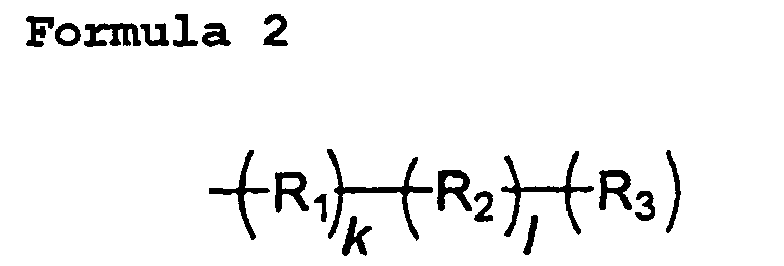
- R is represented by the following Formula 2:
- R 1 is selected from the following group I in which n is an integer of 0 to 10:
- R 2 is a photo-alignment group selected from the groups II and III and, when l is 2 or more, at least one of R 2 is selected from the group II;
- R 3 is a hydrogen atom or is selected from the group IV in which X shows a hydrogen atom, an alkyl or alkoxy group of 1 to 13 carbon atoms, an aromatic group of 6 to 20 carbon atoms, a heteroaromatic group of 4 to 14 carbon atoms having a heteroatom contained in an aromatic ring, (OCH 2 ) p CH 3 (wherein p is an integer of 0 to 12), F, or Cl, and m is an integer of 0 to 18: k is an integer of 0 to 3
- an organic thin film transistor comprising a gate electrode - a gate insulating film - an organic active film - a source/drain electrode - a protection film deposited sequentially on a substrate, or a gate electrode - a gate insulating film - a source/drain electrode - an organic active film - a protection film deposited sequentially on a substrate, wherein the gate insulating film comprises the organic insulating polymer of Formula 1.
- an organic gate insulating film includes an organic insulating polymer as represented by the following Formula 1:
- R is represented by the following Formula 2: wherein, R 1 is selected from the following group I in which n is an integer of 0 to 10: R 2 is a photo-alignment group selected from the groups II and III and, when 1 is 2 or more, at least one of R 2 is selected from the group II; R 3 is a hydrogen atom or is selected from the group IV in which X shows a hydrogen atom, an alkyl or alkoxy group of 1 to 13 carbon atoms, an aromatic group of 6 to 20 carbon atoms, a heteroaromatic group of 4 to 14 carbon atoms having a heteroatom contained in an aromatic ring, (OCH 2 ) p CH 3 (wherein p is an integer of 0 to 12), F, or Cl, and m is an integer of 0 to 18: k is an integer of 0 to 3; 1 is an integer of 1 to 5; and R 1 and
- the gate insulting film of the present invention is characterized in that a photo-alignment group is introduced into the organic insulating polymer used for the insulating film, so that alignment (or orientation) of an organic active film increase largely, thereby improving charge mobility. Also, by providing good condition for the formation of the organic active film, the organic insulating film of the present invention can contribute to obtain larger grain size in the organic active film, compared with the conventional inorganic insulating films.
- the organic insulating polymer film of the present invention has the surface energy of 35 to 50 mN/m, and, judging from this, the surface energy is believed to have an effect on the grain size of organic active film by affecting the degree of crystallization when the organic active film being formed.
- the organic thin film transistor of the present invention includes the organic insulating polymer as the insulating film, and is composed of, but not limited to, a generally known structure, that is, substrate/gate electrode/gate insulating film/organic active film/source-drain electrode or substrate/gate electrode/gate insulating film/source-drain electrode/organic active film.
- the organic active film is formed of a generally used material, but not limited to, for example, pentacene, copper phthalocyanine, polythiophene, polyaniline, polyacetylene, polypyrrole, polyphenylenevinylene or derivatives thereof.
- the gate electrode is made of a generally used metal, but not limited to, for example, gold (Au), silver (Ag), nickel (Ni), indium tin oxide (ITO), aluminum (Al), chromium (Cr), etc.
- the source and drain electrodes are made of a generally used metal, but being not limited to, for example, gold (Au), silver (Ag), nickel (ni), indium tin oxide (ITO), chromium (Cr), etc.
- EXAMPLE 1 Fabrication of Organic Thin Film Transistor including Organic Insulating Polymer (S1) as Gate Insulating Film and Pentacene as Active film
- An organic thin film transistor having a structure shown in FIG. 1 was fabricated by use of an organic insulating polymer (S1) represented by the following Formula 7:
- a silicon oxide film was deposited at a thickness of 3000 ⁇ with CVD (Chemical Vapor Deposition). Then, a 2000 ⁇ thick gate electrode of aluminum (Al) was formed on the silicon oxide film using a method of vapor deposition. Thereafter, 10wt% solution of organic insulating polymer (S1) dissolved in NMP was coated on the gate electrode by a spin coating process at 1000 rpm to obtain a thickness of 7000 ⁇ , and then baked at 100°C for 1 hour in a nitrogen atmosphere.
- CVD Chemical Vapor Deposition
- pentacene was deposited at a thickness of 700 ⁇ under the conditions of a vacuum of 2 ⁇ 10 -6 torr, a substrate temperature of 80°C and a deposition rate of 0.3 ⁇ /sec, by OMBD (Organic Molecular Beam Deposition), thereby forming a pentacene active film on the organic insulating polymer film.
- OMBD Organic Molecular Beam Deposition
- a source-drain electrode of gold (Au) was formed on the pentacene active film by vapor deposition, with using a shadow mask with a channel length of 100 ⁇ m and a channel width of 2 mm.
- organic thin film transistor of top contact type was fabricated as shown in FIG. 1.
- 1 denotes a substrate
- 2 denotes a gate electrode
- 3 denotes an organic gate insulating film
- 4 denotes a source electrode
- 5 denotes a drain electrode
- 6 denotes an organic active film.
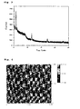
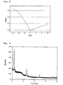
- FIG. 3 An XRD graph of a pentacene thin film formed on the organic insulating polymer (S1) is shown in FIG. 3, an AFM image thereof is seen in FIG. 4 and a current transfer curve of the fabricated organic thin film transistor is shown in FIG. 5:
- EXAMPLE 2 Fabrication of Organic Thin Film Transistor including Organic Insulating Polymer (S2) as Gate Insulating Film and Pentacene as Active film
- An organic thin film transistor having a structure shown in FIG. 1 was fabricated by use of an organic insulating polymer (S2) represented by the following Formula 8:
- FIG. 6 An XRD graph of a pentacene thin film formed on the organic insulating polymer (S2) is shown in FIG. 6, an AFM image thereof is shown in FIG 7, and a current transfer curve of the fabricated organic thin film transistor is shown in FIG. 8.
- EXAMPLE 3 Fabrication of Organic Thin Film Transistor including Organic Insulating Polymer (S3) as Gate Insulating Film and Pentacene as Active film
- An organic thin film transistor having a structure shown in FIG. 1 was fabricated by use of an organic insulating polymer (S3) represented by the following Formula 9:
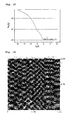
- FIG. 9 An XRD graph of a pentacene thin film formed on the organic insulating polymer (S3) is shown in FIG. 9, an AFM image thereof is shown in FIG 10, and a current transfer curve of the fabricated organic thin film transistor is shown in FIG. 11.
- EXAMPLE 4 Fabrication of Organic Thin Film Transistor including Organic Insulating Polymer (S4) as Gate Insulating Film and Pentacene as Active film
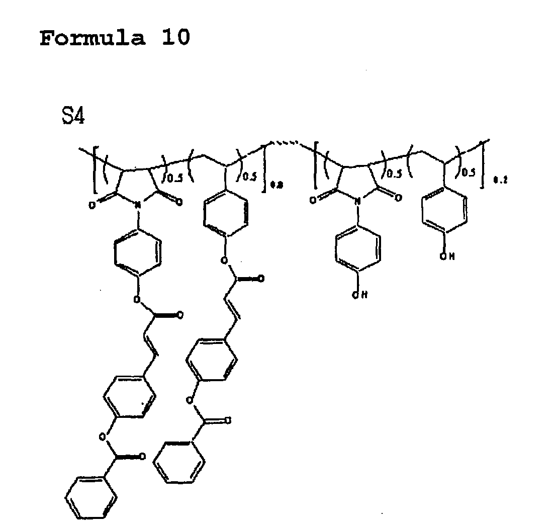
- An organic thin film transistor having a structure shown in FIG. 1 was fabricated by use of an organic insulating polymer (S4) represented by the following Formula 10:
- FIG. 12 An XRD graph of a pentacene thin film formed on the organic insulating polymer (S4) is shown in FIG. 12, an AFM image thereof is shown in FIG 13, and a current transfer curve of the fabricated organic thin film transistor is shown in FIG. 14.
- EXAMPLE 5 Fabrication of Organic Thin Film Transistor including Organic Insulating Polymer (S1) as Gate Insulating Film and P3HT of conductive polymer as Active film
- an organic thin film transistor was fabricated in the same way of Example 1. Specifically, 5wt% solution of the conductive polymer, Poly(3hexylthiopene-2,5-diyl)[P3HT], dissolved in chloroform was coated by a spin coating process at 2000 rpm to obtain a thickness of 2160 ⁇ , and then baked at 100°C for 1 hour in a nitrogen atmosphere to form a organic active layer.
- the P3HT was purchased from Aldrich co. Ltd and subjected to further purification before use.
- the pentacene thin film of the present invention can be successfully fabricated.
- the pentacene thin film as the organic active film deposited on the organic insulating film has a grain size of about 2 to 3 ⁇ m, which is two to three times larger than 1 ⁇ m, a grain size of a thin film obtained by treating the surface of an inorganic thin film with self-assembly materials, OctadecylTrichlororoSilane (hereinafter, OTS).
- OTS OctadecylTrichlororoSilane
- Organic thin film transistor of bottom contact type as shown in FIG. 2 was fabricated (without OTS film).
- a surface of a Si wafer substrate was treated by RCA washing process, a wet-chemical washing process widely used for a semiconductor process.
- the substrate was high-level doped p+-Si, and a doped Si was used as a gate.
- a thermal oxidation process a 992 ⁇ -thick SiO 2 layer was grown on the substrate and then washed with the RCA process. Thereafter, a baking process accompanying dehydration was performed at 100°C for 15 min.
- SiO 2 was partially etched according to the following procedures: First, hexamethyldisilazane was coated on a SiO 2 substrate with a spin-coater (RAURELL, WS-400-6NPP) at 3000 rpm for 10 sec and a photoresist (Positive PR Az 1512) was coated thereon at 2000 rpm for 15 sec and then subjected to a soft-baking at 100°C for 15 min.
- RAURELL, WS-400-6NPP spin-coater
- a photoresist Positive PR Az 1512
- an exposing process was performed for 40 sec through an optical mask for use in the formation of partially etched windows by use of a mask aligner (Karlsuss, MJB 3), after which a developing process was carried out using a developer (AZ 300 MIF Developer, Clariant). Then, the developer remaining on the substrate was eliminated by using deionized water and residual moisture thereon was removed by N 2 gas, and then a hard-baking process was performed at 100°C for 15 min.
- BHF buffered HF
- NH 4 F a mixture of HF, deionized water and NH 4 F at a ratio of 1:3:3 was prepared and used for etching an oxide film thereby a gate was formed.
- the photoresist was coated again and a baked to form source-drain patterns through a lift-off process.
- the source-drain electrode Au was used because it is known to be easily deposited with thermal deposition and to have a high work function of 5.1 eV.
- a 700 ⁇ thick pentacene film was deposited onto a device on which source-drain formed through OMBD method, under the conditions of a vacuum of 2 ⁇ 10 -6 torr, a substrate temperature of 80°C and a deposition rate of 0.3 ⁇ /sec by using a shadow mask with a channel length of 10 ⁇ m and a channel width of 2mm.
- the organic thin film transistor thus obtained had an invert-coplanar structure as shown in FIG. 2.
- the gate electrode was positioned on an opposite side of the source and drain electrodes on which the pentacene active film was deposited.
- Commercially available pentacene powders Aldrich Co. Ltd., 99.8% were used without further purification.
- 3 denotes gate insulating film of SiO 2 .
- the AFM image of the pentacene thin film is shown in FIG. 16, and the current transfer curve of the fabricated organic thin film transistor is seen in FIG. 17.
- COMPARATIVE EXAMPLE 2 Fabrication of Organic Thin Film Transistor including OTS-Surface Treated SiO 2 as Gate Insulating Film and Pentacene as Active film
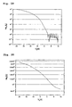
- the AFM image of the fabricated pentacene thin film is shown in FIG. 18, and the current transfer curve of the fabricated transistor is shown in FIG. 19.
- COMPARATIVE EXAMPLE 3 Fabrication of Organic Thin Film Transistor including OTS-Surface Treated SiO 2 as Gate Insulating Film and Conductive Polymer P3HT as Active film
- an organic thin film transistor was fabricated in the same way of Comparative Example 2. Specifically, 1wt% solution of P3HT dissolved in chloroform was coated by a spin coating process at 2000 rpm to obtain a thickness of 2160 ⁇ , and then baked at 100°C for 1 hour in a nitrogen atmosphere to form a organic active layer.
- the current transfer curve of the fabricated organic thin film transistor is shown in FIG. 20.
- each of test pieces was placed on a stage.
- Deionized water, diiodomethane and formamide were separately injected into three syringes, one of which was positioned upward to be perpendicular to the test piece.
- a distance and a focus of a microscope were adjusted and the stage was controlled right and left in order for a tip of a needle of the syringe to be seen along with the test piece in the monitor.
- the liquid in the syringe was added dropwise on the stage.
- a baseline was adjusted and a contact angle was measured.
- the other two liquids were measured for contact angles in the same manner.
- the contact angles measured using the three liquids were analyzed with an analytic program (Drop shape analysis (DSA), ver. 1.70.0.81, KRUSS), to calculate the surface energy.
- DSA Drop shape analysis
- KRUSS KRUSS
- the grain sizes were determined by averaging the values obtained with reference to the scales shown in the AFM images of the pentacene thin films deposited on the organic insulating films.
- Grain size 1 S1 Pentacene 46.1 1.80 -2.5 2 S2 Pentacene 38.3 0.33 -2.5 3 S3 Pentacene 38.6 0.22 -2 4 S4 Pentacene 38.3 0.43 ⁇ 2 C. 1 SiO 2 Pentacene 57.0 0.01 >1 C. 2 SiO 2 (OTS) Pentacene 37.1 0.3 ⁇ 1 5 S1 P3HT 46.1 0.6 - C. 3 SiO 2 (OTS) P3HT 37.1 0.01 -
- the present invention provides an organic gate insulating film and an organic thin film transistor fabricated using the same.
- the organic active film formed on the organic insulating film has larger grain sizes, compared to that of an organic active film formed on a conventional inorganic insulating film.
- the transistor of the present invention has very high mobility.
Landscapes
- Thin Film Transistor (AREA)
- Electroluminescent Light Sources (AREA)
- Addition Polymer Or Copolymer, Post-Treatments, Or Chemical Modifications (AREA)
- Formation Of Insulating Films (AREA)
Abstract
Description





m is a real number of 0.3 to 0.7 and n is a real number of 0.3 to 0.7, while the sum of m and n is 1; x is a real number of 0.3 to 0.7 and y is a real number of 0.3 to 0.7, while the sum of x and y is 1; and i is a real number of 0 to 1 and j is a real number of 0 to 1, while the sum of i and j is 1.
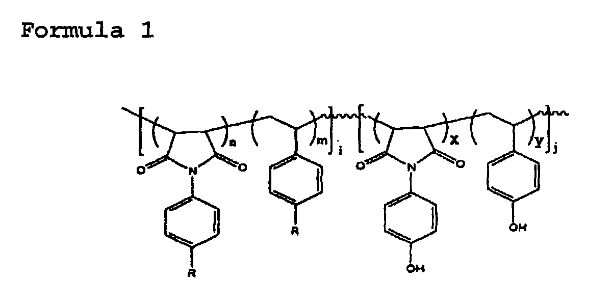
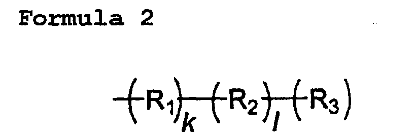


m is a real number of 0.3 to 0.7 and n is a real number of 0.3 to 0.7, while the sum of m and n is 1; x is a real number of 0.3 to 0.7 and y is a real number of 0.3 to 0.7, while the sum of x and y is 1; and i is a real number of 0 to 1 and j is a real number of 0 to 1, while the sum of i and j is 1.

- XRD graph: measured using APD 1700 available from KRUSS Co. Ltd.
- AFM image: measured using AutoProbe CP Research available from PSIA Co. Ltd.
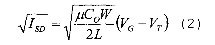
- Current transfer curve: measured using Semiconductor parameter analyzer HP4155A available from Hewlett Packard Co. Ltd.


| Gate Ex.No. | Insul. Film | Active film | Surface Energy of Insul. Film (mN/m) | Mobility (cm2/Vs) | Grain size |
| 1 | S1 | Pentacene | 46.1 | 1.80 | -2.5 |
| 2 | S2 | Pentacene | 38.3 | 0.33 | -2.5 |
| 3 | S3 | Pentacene | 38.6 | 0.22 | -2 |
| 4 | S4 | Pentacene | 38.3 | 0.43 | ∼2 |
| C. 1 | SiO2 | Pentacene | 57.0 | 0.01 | >1 |
| C. 2 | SiO2(OTS) | Pentacene | 37.1 | 0.3 | ∼1 |
| 5 | S1 | P3HT | 46.1 | 0.6 | - |
| C. 3 | SiO2(OTS) | P3HT | 37.1 | 0.01 | - |
Claims (6)
- An organic gate insulating film comprising an organic insulating polymer as represented by the following Formula 1:wherein, R is represented by the following Formula 2:
 wherein, R1 is selected from the following group I in which n is an integer of 0 to 10:
 R2 is a photo-alignment group selected from the groups II and III and, when ℓ is 2 or more, at least one of R2 is selected from the group II;
 R3 is a hydrogen atom or is selected from the group IV in which X represents a hydrogen atom, an alkyl or alkoxy group of 1 to 13 carbon atoms, an aromatic group of 6 to 20 carbon atoms, a heteroaromatic group of 4 to 14 carbon atoms having a heteroatom contained in an aromatic ring, (OCH2)pCH3 (wherein p is an integer of 0 to 12), F, or Cl,
and m is an integer of 0 to 18:k is an integer of 0 to 3; ℓ is an integer of 1 to 5; and R1 and R2 are different respectively when R1 and R2 includes a plurality of functional groups;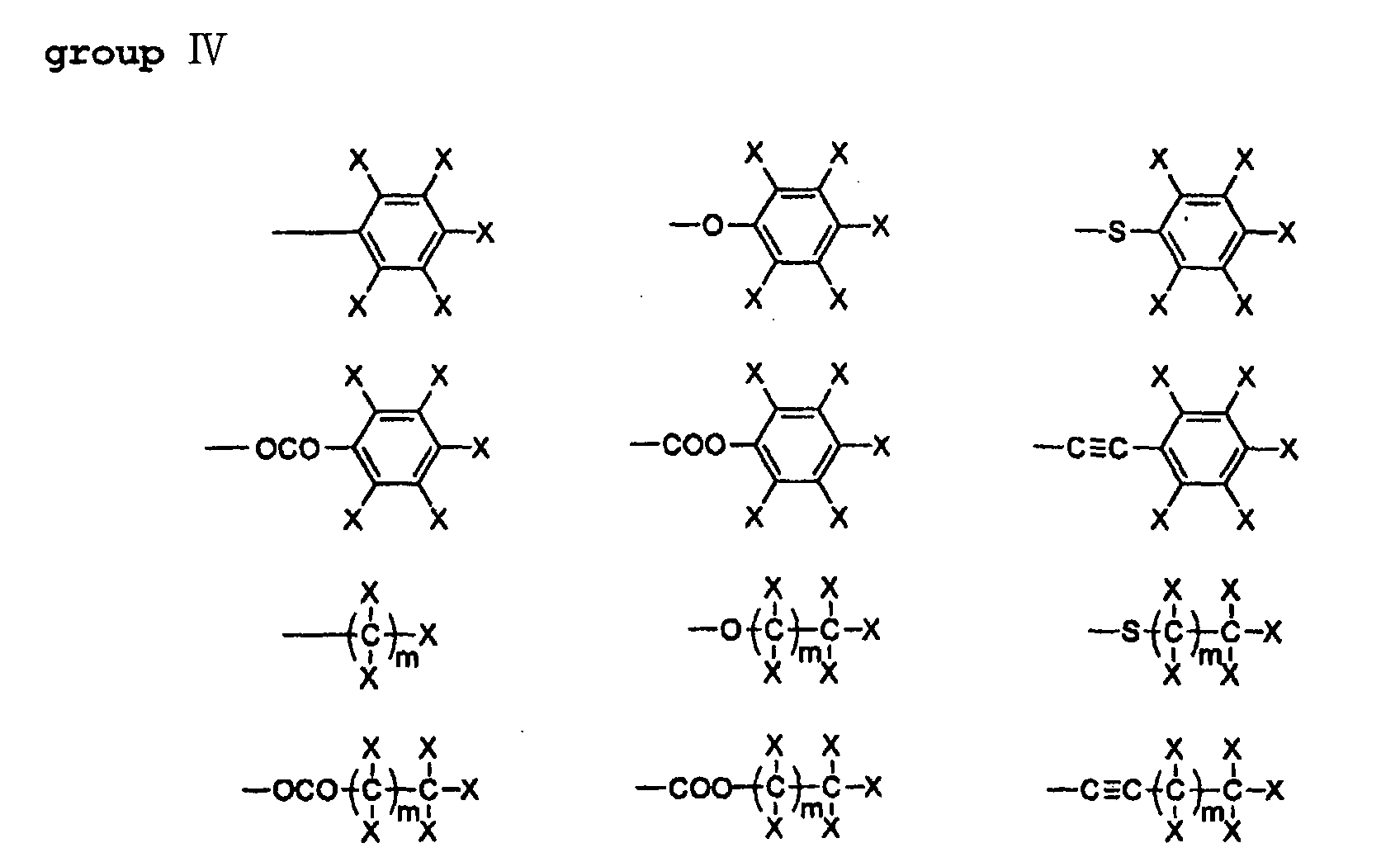
m is a real number of 0.3 to 0.7 and n is a real number of 0.3 to 0.7, with the proviso that the sum of m and n is 1; x is a real number of 0.3 to 0.7 and y is a real number of 0.3 to 0.7, with the proviso that the sum of x and y is 1; and i is a real number of 0 to 1 and j is a real number of 0 to 1, while the sum of i and j is 1. - The organic gate insulating film according to Claim 1, wherein the organic insulating polymer is represented by Formula 11:(wherein, m is a real number of 0.3 to 0.7, n is a real number of 0.3 to 0.7, and m+n is 1).

- An organic thin film transistor formed by laminating, sequentially on a substrate, a gate electrode, a gate insulating film, an organic active film, a source/drain electrode and a protection film, or laminating, sequentially on a substrate, a gate electrode, a gate insulating film, a source/drain electrode, an organic active film and a protection film, wherein the gate insulating film is as claimed in Claim 1 or 2.
- The organic thin film transistor according to Claim 3, wherein the organic gate insulating film is formed by printing, spin coating or dip coating.
- The organic thin film transistor according to Claim 3 or 4, wherein the organic active film is selected from the group consisting of pentacene, copper phthalocyanine, polythiophene, polyaniline, polyacetylene, polypyrrole, polyphenylenevinylene, and derivatives thereof.
- The organic thin film transistor according to any of Claims 3 to 5, wherein the gate electrode is made of gold (Au), silver (Ag), nickel (Ni), indium tin oxide (ITO), aluminum (Al), or chromium (Cr) and the source and drain electrodes are made of gold (Au), silver (Ag), nickel (ni), indium tin oxide (ITO), or chromium (Cr).
Applications Claiming Priority (2)
| Application Number | Priority Date | Filing Date | Title |
|---|---|---|---|
| KR2002059061 | 2002-09-28 | ||
| KR10-2002-0059061A KR100524552B1 (en) | 2002-09-28 | 2002-09-28 | Organic Gate Insulating Film And Organic Thin Film Transistor Using The Same |
Publications (2)
| Publication Number | Publication Date |
|---|---|
| EP1416548A2 true EP1416548A2 (en) | 2004-05-06 |
| EP1416548A3 EP1416548A3 (en) | 2005-12-07 |
Family
ID=32040941
Family Applications (1)
| Application Number | Title | Priority Date | Filing Date |
|---|---|---|---|
| EP03255924A Withdrawn EP1416548A3 (en) | 2002-09-28 | 2003-09-22 | Organic gate insulating film and organic thin film transistor using the same |
Country Status (5)
| Country | Link |
|---|---|
| US (1) | US6849870B2 (en) |
| EP (1) | EP1416548A3 (en) |
| JP (1) | JP4304033B2 (en) |
| KR (1) | KR100524552B1 (en) |
| TW (1) | TW200404824A (en) |
Cited By (2)
| Publication number | Priority date | Publication date | Assignee | Title |
|---|---|---|---|---|
| CN100414414C (en) * | 2004-06-14 | 2008-08-27 | 三星电子株式会社 | Organic thin film transistor array panel and manufacturing method thereof |
| EP2048171A4 (en) * | 2006-08-04 | 2013-10-16 | Mitsubishi Chem Corp | INSULATING LAYER, ELECTRONIC DEVICE, FIELD EFFECT TRANSISTOR, AND POLYVINYLTHIOPHENOL |
Families Citing this family (41)
| Publication number | Priority date | Publication date | Assignee | Title |
|---|---|---|---|---|
| KR20050058062A (en) | 2003-12-11 | 2005-06-16 | 삼성전자주식회사 | Composition for preparing organic insulating film and the organic insulating film prepared by using the same |
| KR100560796B1 (en) * | 2004-06-24 | 2006-03-13 | 삼성에스디아이 주식회사 | Organic thin film transistor and its manufacturing method |
| WO2006016669A1 (en) * | 2004-08-13 | 2006-02-16 | Semiconductor Energy Laboratory Co., Ltd. | Method for manufacturing semiconductor device |
| JP4858804B2 (en) * | 2004-08-31 | 2012-01-18 | 国立大学法人大阪大学 | Thin layer chemical transistor and manufacturing method thereof |
| KR100606655B1 (en) | 2004-09-22 | 2006-08-01 | 한국전자통신연구원 | Photoreactive organic polymer gate insulating film composition and organic thin film transistor using the same |
| KR100668407B1 (en) * | 2004-10-15 | 2007-01-16 | 한국전자통신연구원 | Photoreactive organic polymer gate insulating film composition and organic thin film transistor using the same |
| KR100683685B1 (en) | 2004-10-28 | 2007-02-15 | 삼성에스디아이 주식회사 | Organic light emitting display device having organic thin film transistor and manufacturing method thereof |
| JP4502382B2 (en) * | 2004-11-02 | 2010-07-14 | キヤノン株式会社 | Organic transistor |
| KR100593300B1 (en) * | 2004-11-10 | 2006-06-26 | 한국전자통신연구원 | Thermosetting organic polymer gate insulating film composition and organic thin film transistor using same |
| KR100603393B1 (en) | 2004-11-10 | 2006-07-20 | 삼성에스디아이 주식회사 | Organic thin film transistor, its manufacturing method and organic light emitting display device comprising organic thin film transistor |
| KR101192615B1 (en) * | 2004-11-11 | 2012-10-18 | 미쓰비시 가가꾸 가부시키가이샤 | Field effect transistor |
| KR101112541B1 (en) * | 2004-11-16 | 2012-03-13 | 삼성전자주식회사 | Thin film transistor array panel using organic semiconductor and manufacturing method thereof |
| JP4865999B2 (en) | 2004-11-19 | 2012-02-01 | 株式会社日立製作所 | Method for manufacturing field effect transistor |
| EP1670079B1 (en) | 2004-12-08 | 2010-12-01 | Samsung Mobile Display Co., Ltd. | Method of forming a conductive pattern of a thin film transistor |
| US7768014B2 (en) * | 2005-01-31 | 2010-08-03 | Semiconductor Energy Laboratory Co., Ltd. | Memory device and manufacturing method thereof |
| KR100719547B1 (en) | 2005-03-24 | 2007-05-17 | 삼성에스디아이 주식회사 | Organic thin film patterning method, organic thin film transistor using same, manufacturing method thereof and flat panel display device comprising organic thin film transistor |
| US20060231908A1 (en) * | 2005-04-13 | 2006-10-19 | Xerox Corporation | Multilayer gate dielectric |
| KR100647693B1 (en) | 2005-05-24 | 2006-11-23 | 삼성에스디아이 주식회사 | Organic thin film transistor, its manufacturing method and organic light emitting display device comprising organic thin film transistor |
| KR100647695B1 (en) | 2005-05-27 | 2006-11-23 | 삼성에스디아이 주식회사 | Organic thin film transistor, manufacturing method thereof and flat panel display device having same |
| KR101219048B1 (en) * | 2005-07-14 | 2013-01-09 | 삼성디스플레이 주식회사 | Flat panel display and method of making flat panel display |
| KR100647704B1 (en) * | 2005-09-26 | 2006-11-23 | 삼성에스디아이 주식회사 | Organic thin film transistor, flat panel display device having same, manufacturing method of organic thin film transistor and manufacturing method of flat panel display device |
| KR101186740B1 (en) | 2006-02-17 | 2012-09-28 | 삼성전자주식회사 | Method for Fabricating Bank and Organic Thin Film Transistor Having the Bank |
| KR101249097B1 (en) | 2006-05-04 | 2013-03-29 | 삼성전자주식회사 | Composition for Organic Gate Insulator, Method for Fabricating Organic Gate Insulator and Organic Thin Film Transistor Having the Same |
| KR100777739B1 (en) * | 2006-05-26 | 2007-11-19 | 삼성에스디아이 주식회사 | A thin film transistor, a method of manufacturing the same, and a flat panel display device having the thin film transistor |
| KR101198218B1 (en) * | 2006-06-19 | 2012-11-07 | 엘지디스플레이 주식회사 | Array substrate for liquid crystal display device and method for fabricating the same |
| US20080161464A1 (en) * | 2006-06-28 | 2008-07-03 | Marks Tobin J | Crosslinked polymeric dielectric materials and methods of manufacturing and use thereof |
| JP5470686B2 (en) * | 2006-08-04 | 2014-04-16 | 三菱化学株式会社 | Insulating layer, electronic device, field effect transistor, and polyvinyl thiophenol |
| KR100737383B1 (en) | 2006-09-11 | 2007-07-09 | 한국전자통신연구원 | Insulating film, organic thin film transistor using the same, and manufacturing method |
| KR101224723B1 (en) * | 2006-09-15 | 2013-01-21 | 삼성전자주식회사 | Composition for Preparing Organic Insulating Film and Organic Insulating Layer and Organic Thin Film Transistor Prepared by Using the Same |
| KR101151106B1 (en) * | 2006-09-15 | 2012-06-01 | 삼성전자주식회사 | Organic Insulating Polymer and Organic Insulating Layer and Organic Thin Film Transistor Prepared by using the Same |
| JP5196215B2 (en) * | 2006-09-29 | 2013-05-15 | ソニー株式会社 | Semiconductor device |
| ES2525040T3 (en) | 2006-11-28 | 2014-12-16 | Polyera Corporation | Dielectric materials based on photopolymer and methods of preparation and use thereof |
| KR20090065254A (en) | 2007-12-17 | 2009-06-22 | 한국전자통신연구원 | Photoreactive Organic Polymer Gate Insulator Composition and Organic Thin Film Transistor Using the Same |
| KR101004734B1 (en) * | 2008-07-29 | 2011-01-04 | 한국전자통신연구원 | Organic thin film transistor manufacturing method using surface energy control |
| KR101069585B1 (en) | 2009-01-15 | 2011-10-05 | 포항공과대학교 산학협력단 | Surface treated substrate for ink-jec printing |
| JP5605097B2 (en) * | 2010-09-03 | 2014-10-15 | ソニー株式会社 | Manufacturing method of electronic device |
| US20160141530A1 (en) * | 2013-06-11 | 2016-05-19 | Sharp Kabushiki Kaisha | Semiconductor element and semiconductor element manufacturing method |
| JP6034326B2 (en) * | 2014-03-26 | 2016-11-30 | 富士フイルム株式会社 | Semiconductor device and composition for forming insulating layer |
| KR101811617B1 (en) | 2015-07-21 | 2017-12-26 | 부산대학교 산학협력단 | Thermo-Crosslikable Insulating Polymers and Organic Thin-Film Transistor Using the Same |
| JPWO2017038948A1 (en) * | 2015-09-02 | 2018-06-28 | 富士フイルム株式会社 | Organic thin film transistor, organic thin film transistor manufacturing method, organic semiconductor composition, organic semiconductor film, and organic semiconductor film manufacturing method |
| CN111602087B (en) * | 2018-04-19 | 2023-03-24 | Jsr株式会社 | Liquid crystal aligning agent, liquid crystal alignment film, liquid crystal element, polymer and compound |
Family Cites Families (16)
| Publication number | Priority date | Publication date | Assignee | Title |
|---|---|---|---|---|
| FR2664430B1 (en) * | 1990-07-04 | 1992-09-18 | Centre Nat Rech Scient | THIN FILM FIELD EFFECT TRANSISTOR WITH MIS STRUCTURE, IN WHICH THE INSULATION AND THE SEMICONDUCTOR ARE MADE OF ORGANIC MATERIALS. |
| US5556706A (en) * | 1993-10-06 | 1996-09-17 | Matsushita Electric Industrial Co., Ltd. | Conductive layered product and method of manufacturing the same |
| US6107117A (en) * | 1996-12-20 | 2000-08-22 | Lucent Technologies Inc. | Method of making an organic thin film transistor |
| US5981970A (en) * | 1997-03-25 | 1999-11-09 | International Business Machines Corporation | Thin-film field-effect transistor with organic semiconductor requiring low operating voltages |
| US5946551A (en) * | 1997-03-25 | 1999-08-31 | Dimitrakopoulos; Christos Dimitrios | Fabrication of thin film effect transistor comprising an organic semiconductor and chemical solution deposited metal oxide gate dielectric |
| US6344662B1 (en) * | 1997-03-25 | 2002-02-05 | International Business Machines Corporation | Thin-film field-effect transistor with organic-inorganic hybrid semiconductor requiring low operating voltages |
| KR100261119B1 (en) * | 1997-04-18 | 2000-08-01 | 김순택 | Optical alignment polymer |
| JPH1131690A (en) * | 1997-07-11 | 1999-02-02 | Matsushita Electric Ind Co Ltd | Method of forming porous film |
| JP3756666B2 (en) * | 1998-05-08 | 2006-03-15 | 松下電器産業株式会社 | Method for forming porous film and apparatus for forming the same |
| KR100279043B1 (en) * | 1998-07-15 | 2001-01-15 | 윤종용 | Polymaleimide and Polyimide Photoalignment Material for Liquid Crystal Display |
| US6215130B1 (en) * | 1998-08-20 | 2001-04-10 | Lucent Technologies Inc. | Thin film transistors |
| US6207472B1 (en) * | 1999-03-09 | 2001-03-27 | International Business Machines Corporation | Low temperature thin film transistor fabrication |
| KR100425242B1 (en) * | 2000-05-29 | 2004-03-30 | 주식회사 엘지화학 | Dielectrics material for layer of semiconductor and semiconductor device using the same |
| KR100373215B1 (en) * | 2001-02-01 | 2003-02-25 | 주식회사 엘지화학 | Method for preparing low dielectric materials for semiconductor ic device |
| JP4841751B2 (en) * | 2001-06-01 | 2011-12-21 | 株式会社半導体エネルギー研究所 | Organic semiconductor device and manufacturing method thereof |
| US6777529B2 (en) * | 2002-01-11 | 2004-08-17 | Xerox Corporation | Polythiophenes and devices thereof |
-
2002
- 2002-09-28 KR KR10-2002-0059061A patent/KR100524552B1/en not_active Expired - Fee Related
-
2003
- 2003-09-09 TW TW092124879A patent/TW200404824A/en unknown
- 2003-09-09 US US10/657,191 patent/US6849870B2/en not_active Expired - Lifetime
- 2003-09-22 EP EP03255924A patent/EP1416548A3/en not_active Withdrawn
- 2003-09-24 JP JP2003331767A patent/JP4304033B2/en not_active Expired - Fee Related
Cited By (4)
| Publication number | Priority date | Publication date | Assignee | Title |
|---|---|---|---|---|
| CN100414414C (en) * | 2004-06-14 | 2008-08-27 | 三星电子株式会社 | Organic thin film transistor array panel and manufacturing method thereof |
| US7993958B2 (en) | 2004-06-14 | 2011-08-09 | Samsung Electronics Co., Ltd. | Organic thin film transistor array panel and manufacturing method thereof |
| US8389992B2 (en) | 2004-06-14 | 2013-03-05 | Samsung Display Co., Ltd. | Organic thin film transistor array panel and manufacturing method thereof |
| EP2048171A4 (en) * | 2006-08-04 | 2013-10-16 | Mitsubishi Chem Corp | INSULATING LAYER, ELECTRONIC DEVICE, FIELD EFFECT TRANSISTOR, AND POLYVINYLTHIOPHENOL |
Also Published As
| Publication number | Publication date |
|---|---|
| KR100524552B1 (en) | 2005-10-28 |
| US6849870B2 (en) | 2005-02-01 |
| US20040065929A1 (en) | 2004-04-08 |
| JP4304033B2 (en) | 2009-07-29 |
| TW200404824A (en) | 2004-04-01 |
| EP1416548A3 (en) | 2005-12-07 |
| KR20040028010A (en) | 2004-04-03 |
| JP2004115805A (en) | 2004-04-15 |
Similar Documents
| Publication | Publication Date | Title |
|---|---|---|
| EP1416548A2 (en) | Organic gate insulating film and organic thin film transistor using the same | |
| EP0852403A1 (en) | Method of making an organic thin film transistor | |
| US20060234430A1 (en) | Tft fabrication process | |
| JPH10270712A (en) | Structure of thin film transistor device | |
| US7675059B2 (en) | Copolymer, organic insulating layer composition, and organic insulating layer and organic thin film transistor manufactured using the same | |
| EP1542241B1 (en) | Composition for forming organic insulating film and organic insulating film formed from the same | |
| KR100477394B1 (en) | Thin-film field-effect transistor with organic-inorganic hybrid semiconductor requiring low operating voltages | |
| US20050110008A1 (en) | Organic thin film transistor comprising buffer layer | |
| US9721697B2 (en) | Organic polymeric bi-metallic composites | |
| US20060231829A1 (en) | TFT gate dielectric with crosslinked polymer | |
| KR100593300B1 (en) | Thermosetting organic polymer gate insulating film composition and organic thin film transistor using same | |
| KR101064773B1 (en) | Manufacturing Method of Organic Thin Film Transistor | |
| US7646014B2 (en) | Organic thin film transistor comprising fluorine-based polymer thin film and method for fabricating the same | |
| KR101743753B1 (en) | Surface-modified PEMA insulator, method of modifying surface of PEMA insulator and organic thin film transistor prepared thereby | |
| KR100606655B1 (en) | Photoreactive organic polymer gate insulating film composition and organic thin film transistor using the same | |
| EP1976040B1 (en) | Insulating material for organic field effect transistors | |
| KR100696195B1 (en) | Low Temperature Curing Polymer Gate Insulator and Organic Thin Film Transistor Using the Same | |
| KR100572854B1 (en) | Photoreactive organic polymer gate insulating film composition and organic thin film transistor using the same | |
| KR101075620B1 (en) | Ferroelectric field effect transistor with poly(styrene-r-methylmethacrylate) copolymer as a interlayer and the manufacturing method thereof | |
| US20140124741A1 (en) | Devices containing organic polymeric multi-metallic composites | |
| KR101102222B1 (en) | Method for Preparing an Organic Thin Film Transistor by using Electric Field Treatment | |
| KR20060033391A (en) | Photoreactive organic polymer gate insulating film composition and organic thin film transistor using the same |
Legal Events
| Date | Code | Title | Description |
|---|---|---|---|
| PUAI | Public reference made under article 153(3) epc to a published international application that has entered the european phase |
Free format text: ORIGINAL CODE: 0009012 |
|
| AK | Designated contracting states |
Kind code of ref document: A2 Designated state(s): AT BE BG CH CY CZ DE DK EE ES FI FR GB GR HU IE IT LI LU MC NL PT RO SE SI SK TR |
|
| AX | Request for extension of the european patent |
Extension state: AL LT LV MK |
|
| RIN1 | Information on inventor provided before grant (corrected) |
Inventor name: KANG, IN NAM Inventor name: JEONG, EUN JEONG Inventor name: CHOI, HWAN JAE,104/1402 SAJONG APT. Inventor name: SONG, IN SUNG,204/1503 SEONBIMAEUL APT. Inventor name: KEE, IN SEO,508/801 SSANGYONG APT. Inventor name: KOO, BON WON |
|
| RIN1 | Information on inventor provided before grant (corrected) |
Inventor name: KANG, IN NAM Inventor name: JEONG, EUN JEONG Inventor name: CHOI, HWAN JAE,104/1402 SAJONG APT. Inventor name: SONG, IN SUNG,104/704 HYUNDAI-HOMETOWN 4 CHA Inventor name: KEE, IN SEO,508/801 SSANGYONG APT. Inventor name: KOO, BON WON |
|
| PUAL | Search report despatched |
Free format text: ORIGINAL CODE: 0009013 |
|
| AK | Designated contracting states |
Kind code of ref document: A3 Designated state(s): AT BE BG CH CY CZ DE DK EE ES FI FR GB GR HU IE IT LI LU MC NL PT RO SE SI SK TR |
|
| AX | Request for extension of the european patent |
Extension state: AL LT LV MK |
|
| RIC1 | Information provided on ipc code assigned before grant |
Ipc: 7H 01L 51/20 A |
|
| 17P | Request for examination filed |
Effective date: 20060524 |
|
| AKX | Designation fees paid |
Designated state(s): DE FR GB |
|
| STAA | Information on the status of an ep patent application or granted ep patent |
Free format text: STATUS: THE APPLICATION HAS BEEN WITHDRAWN |
|
| 18W | Application withdrawn |
Effective date: 20090526 |